Note: Descriptions are shown in the official language in which they were submitted.
~~~~.~.4?
FIELD OF THE INVENTION
The present invention relates generally to electrical
switches, and more particularly to a solid state switch
matrix wherein a plurality of switching modules are
connected serially and parallel with each other.
BAGKG1~OUND OF THIS INVENTION
Several types of electronic systems require high
voltage, high current pulses of electrical energy in order
to operate. Usually, the pulses~must have a very fast rise
time and a high frequency rate of repetition. Typically,
the pulses have a rise time of approximately 400
nanoseconds and a frequency of several kilohertz. To
develop 'these output power pulses, a high power switch is
required. Tn these types of electronic systems, the switch
must be able to accommodate an output power pulse of
several thousand volts and a couple hundred amperes.
Presently, such switches for these electronic systems
are constructed using a thyratron tube. The thyratron tube
acts as a switch between high power source and an output
device. The rapid switching of the thyratron tube
modulates the high power source to apply pulses of output
power to the output device. The output pulse is usually
inductively coupled to a load through the secondary winding
of a transformer. In these systems, the switch and
transformer are usually referred to as a "modulator."
In a particular type of electronic system, the load is
typically a high power travelling wave tube. The output
power pulses are applied to the high powered tube. The
tube, as is well known, amplifies a low level microwave
~~~1~~
2
signal. The amplified high power microwave signal may then
be radiated by an antenna.
The basic principle of operation of these modulators
depends upon the storage of electrical energy in the
primary winding of the transformer, and the subsequent
discharge of a fraction or all of the stored energy through
the secondary winding into the high powered vacuum tube.
The type of modulator which discharges all of the stored
energy during each pulse is referred to as a line type
modulator which use pulse forming networks. Modulators
which discharge only a small fraction of the stored energy
are termed hard tube modulators, this term being taken from
the use of the thyratron tube as the switch.
The main disadvantage of the line type modulator is
that they operate at fixed pulse widths, and axe limited in
duty cycle and pulse repetition frequency. Additionally,
their overall reliability is low due to the use of the
thyratron, which exhibits a relatively short: life.
Hard tube modulators are considerably more versatile
with regards to pulse widths, duty cycle and pulse
repetition frequency. However, 'their overall reliability
is even worse than line type modulators due to the higher
current, hence the higher stress, that the thyratron
encounters.
~5 The stress on the thyratron in the hard tube modulator
is from the storage of electrical energy within the primary
winding of the transformer. The primary winding is coupled
in series with t:he switch and the power source. The
switching of current: in the primary winding develaps
considerable voltage and current stresses on the thyratron
tube.
Tn the hard tube modulator, it would be highly
desirable to eliminate the use of the thyratron and replace
it with solid state switch which would take advantage of
the high reliability and long life of solid state
electronics as compared to thyratron tubes. However, a
~~~~.1~~
3
solid state device cannot by itself handle the current and
voltage requirements of the hard tube modulator switch.
SUMMARY OF THE TNVENTTON
It is an object of the present invention to
overcome one or more of the disadvantages and limitations
of the prior art enumerated hereinabove. It is a further
object of the present invention to provide a novel solid
state switch matrix wherein the matrix is formed from a
plurality of switch modules coupled in series and in
parallel with each other to distribute the current and
voltage of the matrix switch substantially across each
module. It is a further object of the present invention to
provide a novel construction for each switch module.
According to the present invention, a solid state
switch matrix for developing a high current, high voltage
output power pulse in response to a small signal input
pulse includes a plurality of solid state switch modules
and a controller. Each of the modules has a small signal
input, a large signal input and a;n output. The modules are
arranged in rows and in columns such that modules in each
of the rows are connected in parallel and modules in each
of the columns are connected in series. The controller has
an input to which the input pulse is applied and develops
a switching pulse for application to the small signal input
of each of the modules in response to the input pulse.
Each of the modules becomes conductive between its large
signal input and its output in response to the switching
pulse. When each module is conductive, the matrix is
conductive between the large signal input of each of the
modules connected in parallel in a first row and the output
of each of the modules connected in parallel in a last row
to develop the output power pulse.
It is an important feature of the present invention
that the modules are electrically balanced such that a
voltage across the matrix is when the matrix is
nonconductive substantially equally distributed across
CA 02061142 2001-11-14
62196-567
4
serially coupled modules and a current through the matrix
when the matrix is conductive is substantially equally
distributed through parallel coupled modules.
In one aspect: of the present invention each module
may be constructed from a MOSFET switch which is turned on,
or becomes conductive, when the switching pulse is applied
to its gate. A Zener diode and a resistor are each coupled
between the source and drain of the MOSFET switch with the
Zener diode and resistor parallel to each other. When the
MOSFET switch is turned off, the resistor acts to equally
divide the total matrix: voltage among the serially coupled
modules. During the snort period of time when the MOSFET
switch transitions from on to off, there will be unequal
voltages across serially coupled modules because of unequal
output capacitance between modules. If this voltage
transient should begin t:o approach a level potentially
damaging to the MOSFET, the Zener diode enters into its
reverse bias breakdown mode, clamping the MOSFET drain to
source voltage at a safe level. Equal current sharing among
parallel coupled modulE~s is accomplished by operating the
MOSFET switch in each module in its saturated mode when on.
The resistance of a MO~~FET switch (in a saturated mode)
increases with increasing current or temperature. Thus,
when a MOSFET switch has a lower :resistance than other
parallel coupled MOSFET switches, it will begin to conduct
proportionally more current. However, the higher current
through the MOSFET results in an increased resistance, with
the extra power dissipation due to the larger current
further increasing the resistance of the MOSFET. The result
of this self-regulating action is that parallel coupled
modules equally distribute the current.
CA 02061142 2001-11-14
62196-567
4a
The invention may be summarized according to one
aspect as a switch matrix for coupling a high voltage, high
current power source to an output device, said switch matrix
comprising: a module having a switch, said switch having a
small signal input, a 7_arge signal input and an output,
wherein said switch is turned on in response to an external
switching pulse applied to said small signal input, said
switch when on causing a voltage to be developed across said
module and a current to be developed through said module;
and a resistor coupled in parallel with said switch between
said large signal input. and said output of said switch; said
module being coupled in series and in parallel with other
modules in said matrix such that when all of said switches
are off said resistor in each module divides the total
voltage across said matrix substantially equally across each
serially coupled modulE>, and such that when all of said
switches are on said switch in each module divides the total
current through said m~W rix substantially equally through
each parallel coupled Module.
According to another aspect the invention provides
a solid state switch matrix for developing a high current,
high voltage output poorer pulse in response to a small
signal input pulse, said switch matrix comprising: a
plurality of solid stage switch modules, each of said
modules having a small signal input, a large signal input
and an output, said modules being arranged in rows and in
columns such that modules in each of said rows are connected
in parallel and module; in each of said columns are
connected in series; and a controller having an input to
which said input pulse is applied, said controller
developing a switching pulse for application to said small
signal input of each of said modules in response to said
CA 02061142 2001-11-14
62196-567
4b
input pulse, each of said modules becoming conductive
between said large signal input and said output in response
to said switching pulse so that said matrix is conductive
between said large signal input of each of said modules
connected in parallel :_n a first one of said rows and said
output of each of said modules connected in parallel in a
last one of said rows too develop said output power pulse
across said solid state switch matrix; said switch modules
being electrically balanced such that when all of said
switch modules are off the total voltage across said matrix
is substantially equala_y divided between each serially
connected switch module, and such that when all of said
switch modules are on t:he total current through said matrix
is substantially equally divided between each parallel
connected switch module.
According to yet another aspect the invention
provides a high output power switching system comprising: a
high power source; a sc>.lid state switch matrix including a
plurality of switch modules and a controller, each of said
modules having a small signal input, a large signal input
and an output, said modules being arranged in rows and
columns such that modules in each of said rows are connected
in parallel and module's in each of said columns are
connected in series, said controller having an input to
which a small signal input pulse is applied and a plurality
of controller outputs, said controller developing a
switching pulse at eacr~ of said controller outputs in
response to said input pulse, each of said plurality of
controller outputs being associated with the respective one
39 of said rows such that said switching pulse at each of said
controller outputs is applied to said small signal input of
said modules in said respective one of said rows, each of
CA 02061142 2001-11-14
62196-567
4c
said modules becoming conductive between said large signal
input and said module output in response to said switching
pulse so that said matrix is conductive between said large
signal input of each oi= said modules connected in parallel
in a first one of said rows and said module output of each
of said modules connected in parallel in a last one of said
rows; and an output device coupled in series with said high
power source and said matrix, said matrix in response to
said switching pulse applied to each of said modules thereof
becoming conductive causing said high power source to couple
a high output power pulse to said output device, said
modules being electric~~lly balanced such that a voltage
across said matrix when nonconductive is substantially
equally distributed across serially coupled modules and a
current through said matrix when conductive is substantially
equally distributed through parallel coupled modules.
These and other advantages and features of the
present invention will become readily apparent to those
skilled in the art from a study of the following Description
of an Exemplary Preferred Embodiment when read in
conjunction with the attached Drawings and appended Claims.
~~a~~~~
BRIEF DESCRIPTION OF THE DRAWING
Fig. 1 is a schematic block diagram of a MOSFET switch
~r~atrix constructed according to the principles of the
present invention:
5 Fig. 2 is a simplified schematic of each switch module
of Fig. 1;
Fig. 3 is a more detailed schematic showing a portion
of the controller and more detail of the switch module; and
Fig. 4 is a schematic diagram showing a typical
application of the switch matrix of Fig. 1.
DESCRIPTION OF AN EXEMPLARY PREFERRED EMBODIMENT
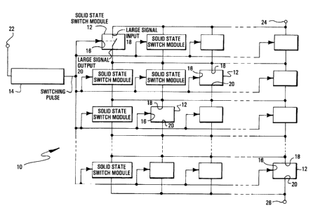
Referring now to Fig. 1, there is shown a switch
matrix 10 constructed according to the principles of the
present invention. As will be described in greater detail
in conjunction with Fig. 4 hereinbelow, the switch matrix
10 is useful for develaping a high current, high voltage
power output power pulse in reaponse to a small signal
input pulse. The switch matrix 7.0 includes a plurality of
solid state switch modules 12 and a controller 14.
Each of the switch modules Z2 has a small signal input
16, a large signal input 18, and an output 20. As best
seen in Fig. 1, each of the modules 12 are arranged in rows
and in columns. The modules 12 in each of the rows are
connected in parallel. Furthermore, the modules 12 in each
of the columns are connected in series.
The controller 14 has an input 22 to which the small
signal input pulse is applied. In response to the input
pulse, the controller 14 develops a switching pulse for
application to the smell signal input 16 of each of the
switch modules 12. When the switching pulse is applied to
each small signal input 16 of the switch modules 12, the
modules 12 become conductive between their large signal
input 18 and their output 19. When each of the modules 12
is conductive, the switch matrix 10 is conductive between
its input terminal 24 and its output terminal 26. The
input terminal 24 of the matrix 10 is connected in parallel
6
with each large signal input 18 of the modules 22 in a
first row of the matrix 10. The output tex-minal 26 is
connected in parallel to the large signal output 20 to the
modules 12 in the last row of the matrix 10.
When the matrix 10 is connected in series to a power
source and an output device, as will be hereinbelow
described in greater detail, the matrix 10 will cause the
energy of the power source to be delivered to the output
device each time an input pulse is applied to the
controller input 22. A resultant current is then developed
in the matrix 10 between its input terminal 24 and output
terminal 26. Each of the modules 12 is electrically
balanced such that this current through the matrix 10 is
substantially equally distributed through parallel coupled
ones of the modules 12.
When the matrix 10 is nonconductive, there is no
current through the matrix 10 ox the output device.
Accordingly, the total power source voltage appears across
the matrix 10, and specifically, across its input 24 and
output 26. The electrical balancing of the modules 12
further divides this voltage equally among serially coupled
ones of the modules 12.
With further reference to lFig. 2, there is shown a
simplified schematic of each switch module 32. In its
basic configuration, the switch module 1.2 includes an n
channel MOSFET switch 28, a Zener diode 30 and a resistor
32.
The MOSFET switch 28 includes a gate 34, a source 36
and a drain 38. The first Zener diode 30 has its anode
coupled to the source 36 of the MOSFET switch 28 and its
cathode coupled to the drain 38 of the MOSFET switch 28.
The resistor 32 is coupled in parallel with the Zener diode
30. The gate 34, the source 36 and the drain 38 of the
Y~OSFET switch 28 are coupled to the respective gate, source
and drain of each other MOSFET switch in parallel coupled
modules in a common row. For serial connection, the source
36 of the ~IOSFET switch 28 is coupled to the drain of the
~~~~1~?
module 12 in a lower row of the matrix 10. Similarly, the
drain 38 of the MOSFET switch 28 is coupled to the source
of the MOSFET switch of the module 12 in an upper row of
the matrix 10. As will be described in greater detail
hereinbelow, the controller 14 develops simultaneously a
switching pulse for application to the small signal input
16 of the modules 12 in each row, and in particular the
gate 34 of the MOSFET switch 28.
With each MOSFET switch 28 off, the resistor 32, being
identical in each module 12, divides the total °°open
circuit" voltage between the matrix input 24 and matrix
output 26 equally among serially coupled ones of the
modules 12. When a positive potential switching pulse is
applied the gate 34 of the MOSFET switch 28, the MOSFET
switch 28 is turned on. With each module 12 in the matrix
10 being simultaneously turned on, the voltage'between the
matrix input 24 and the matrix output 26 goes to
substantially zero causing a voltage to be developed across
the output device and a current to be developed through
each module 12.
It is a feature of the present invention that the
current through each module 12 be substantially equal when
the MOSFET switch 28 is on. Equal current sharing among
parallel coupled modules 12 is accomplished by operating
the MOSFET switch 28 in sack module 12 in its saturated
mode when on. The resistance of the MOSFET switch 28 (in
a saturated mode) increases with increasing current or
temperature. Thus, when one MOSFET switch 28 has a lower
resistance than one of the other parallel coupled MOSFET
switches 28, it will begin to conduct proportionally more
current. However, the higher current through the one
MOSFET switch 28 results in an increased resistance, with
the extra power dissipation due to the larger current
further increasing the resistance of this particular MOSFET
switch 28. The result of this self-regulating action is
that parallel coupled modules 12 equally distribute the
current. During the transition of the MOSFET switch 28 to
~~6~~~~
8
its off state, there will be unequal voltages across
serially coupled modules 12 because of unequal output
capacitance between modules 12. Tf this voltage transient
should begin to approach a level potentially damaging to
the MOSFET switch 28, the Zener diode 30 enters into its
reverse bias breakdown mode, clamping the MOSFET drain to
source voltage at a safe level.
Although the module 12 has been described as being
constructed with a MOSFET switch 28, it is apparent that a
bipolar or ather type of field effect transistor may be
used. Also, the polarity of the transistor used as the
switch may also differ. All that is required is that when
the switching pulse is applied to the small signal input 16
of the module 12, the transistor switch is turned on so
that a voltage may be developed across the module 12 arid a
current enabled therethrough. The first Zener diode 30 may
be connected to this transistor switch so that, when the
switching transistor transistion:~ from on to off, the Zener
diode 30 will prevent excessive switch voltage by going
into Sts reverse breakdown mode.
Referring now to Fig. 3, there is shown a detailed
circuit diagram of the module 12, and a detailed circuit
diagram of a portion of the controller 14. The module 12
may further include a second diode 40, a first gate
resistor 44 and a second gate resistor 46.
The second diode 40 is coupled in series with the
first Zener diode 30. The second diode 40 has its anode
coupled to the gate 38 of the MOSFET switch 28 and its
cathode coupled to the first Zener diode 30. The fourth
diode 42 is in series with the second Zener diode 32.
In general, the second diode 40 is biased to reduce
the effective reverse bias capacitance of the Zener diode
30. Tt is well known that the Zener diode 30 exhibits a
relatively large junction capacitance. The third diode 30
places a relatively small junction capacitance in series
with the junction capacitance of the Zener diode 30.
Therefore, the junction capacitance of the second diode 40
9
approximate the total diode capacitance between the source
36 and drain 38 of the MOSFET switch 28.
The first gate resistor 44 is coupled in series
between the input 16 of the switch module 12 and the gate
34 of the MOSFET switch 28. The second gate resistor 46 is
coupled between the gate 34 of the MOSFET 28 and its source
36. The first gate resistor 44 and second gate resistor 46
are antioscillation resistors. ~Cf the source impedance is
too low, the first gate resistor 44 will prevent self
oscillation. Similarly, the second gate resistor 46 also
prevents oscillation.
The controller 14 includes a transformer 48 and a
plurality of amplifier drivers 50. Tn Fig. 3, one such
amplifier driver is shown. As will become apparent from
the following description, there is one amplifier driver 50
for each row of switch modules 12 within the matrix 10.
The transformer 48 has a primary winding 52 and a
plurality of secondary windings 54. There is one secondary
winding 54 for each row of switch modules 12. Each of the
amplifier drivers 40 is interconnected in series between a
respective secondary winding 54 <~nd the small signal input
16 of the modules 12 in a respective one of the rows of
modules 12.
The primary winding 52 forms the input 22 of the
controller 24. When the input pulse is applied to the
primary winding 52, it is inductively coupled to each of
the secondary winding 54, as is well known. xn response to
the input pulse being coupled to the secondary windings 54,
the amplifier driver 50 connected to each secondary winding
54 develops the switching pulse for its respective row.
Each driver amplifier 50 includes a n-channel MOSFET
56, a p°channel MOSFET 58, a first invertor 60 and a second
invertor 62.
The n-channel MOSFET 56 has a gate 64, a source 66 and
a drain 68. The p°channel MOSFET 58 has a gate 70, a
source 72 and a drain 74. The drain 68 of the n-channel
MOSFET 56 and the drain 74 of the p-channel MOSFET 58 are
10
commonly connected to a node 76. The source 66 of the n-
channel MOSFET 56 is coupled to a reference potential and
the source 72 of the p-channel MOSFET 58 is coupled to a
positive bias potential. The reference potential is the
potential at the source 36 of each of the MOSFET switches
28 coupled to the matrix output 26.
The first inventor 60 is coupled in series between the
secondary winding 54 and the gate 64 of the n-channel
MOSFET 56. Similarly, the second inventor 62 is coupled
between the secondary winding 54 and the gate 70 of the p-
channel MOSFET 58.
As is best seen in Fig. 3, the first inventor 60 is
bias to the reference potential and the second inventor 62.
is biased to the positive bias potential. Since these
inventor are typically fabricated on the same chip, the
output of the first inventor 60 and second inventor 62 will
vary between the reference potential and the positive bias
potential. Interconnected between the first inventor 60
and the gate 64 of the n-channel MOSFET 56 is a gate drive
resistor 77. Similarly, conneci~ed between the output of
the second inventor 62 and the gate 70 of the p-channel
MOSFET 58 is the gate drive resi:~tor 78.
In operation, the n-channel MOSFET 56 and the p
channel MOSFET 58 functioned as serially coupled totem pole
biased transistor switches. In the totem pole biasing, the
n-channel MOSFET 56 is on and the p-channel 58 is off to
couple the reference potential to the node 76 in the
absence of the input pulse. When the input pulse is
applied to the input 22 of the controller 34, and is
coupled through the secondary winding 54, the input of each
of the first inventor 60 and second inventor 62 goes to a
positive potential. The output of each of the first
inventor 60 and second inventor 62 then goes to reference
potential. The reference potential at the gate 64 of the
n-channel MOSFET 56 turns off the MOSFET 56 whereas the
reference potential at the gate 70 at the p-channel MOSFET
58 turns on the MOSFET 58. Therefore, in the presence of
11
the input pulse, the n-channel MOSFET 56 is off and the p
channel MOSFET 58 is on to couple the positive bias
potential to the node 76. The positive potential at the
node 76 is then coupled to the input 16 of the switch
module 12 as the switching pulse.
Of course, the amplifier driver 50 may use other
polarities and other types of transistor switches. ~t is
not necessary that the amplifier driver be of totem pole
configuration. however, the totem pole configuration is
provides rapid switching speeds as is well known.
When the switching pulse developed at node 76 is
coupled to the input 16 of the switch module 12, to cause
'the MOSFET switch 28 to turn on, the power source becomes
coupled to the output device to apply an output power pulse
thereto. The rise time of this output power pulse is
controlled by the current through the first gate resistor
44. The design considerations fox the amplitude of this
current are to achieve a fast rise time of the output power
pulse with minimal overshoot of the output power pulse. To
limit this current, the controller 14 further includes a
resistor 80 coupled in series between the node 76 and the
input 16 of the switch module 1.2. The resistor 80 has a
resistance selected in accordana~e with a desired rise time
of the output power pulse. Coupled in parallel with the
resistor 80 is a diode 82 which is arranged to be reverse
biased when the switching pulse is being developed at the
node 76. When the switching pulse is removed, the diode 82
becomes forward bias thereby shorting out the resistor 80.
By shorting out the resistor 80, the fall time of the
output power pulse is minimized. Minimizing the fall time
of the output power pulse minimizes power dissipation
within the MOSFET switch 28 when the amplifier driver 50 is
being turned off. The controller 1~ may also include a
drive resistor 83, shunt resistor 84 in parallel with each
secondary winding 5~, and a capacitor 85 parallel to
resistor 83.
~~ ~.~.~?
12
With reference now to Fig. 4, there is shown a typical
application of the switch matrix 10 described hereinabove
as used in a high power output power switching system 86.
The power switching system 86 includes a high power source
88, a solid state switch matrix 10 described hereinabove as
having the switch modules l2 and controller 14, and an
output device 90. The output device 90 is coupled in
series with the power source 88 and the switch matrix 10.
With the matrix 10 nonconductive, the voltage of the power
source 88 will be equally divided across serially coupled
ones of the modules 12 for reasons as set forth above.
When the input pulse is applied to the input 22 of the
controller 14, the switching pulse is applied to each of
the switch modules 12 as hereinabove described.
Accordingly, the matrix 10 becomes conductive causing the
power source 88 to couple a high output power pulse to the
output device 90. As described hereinabove, each of the
modules 12 will have a current therethrough which will be
evenly distributed among parallel. coupled modules 12.
The output device 90 may .include a transformer 92
having a load 94. The transformer 92 has a primary winding
96 and a secondary winding 98. The primary winding 96 is
coupled in series between the power source 88 and the input
24 of the switch matrix 10. The load 94 may be coupled in
parallel with the secondary winding 98.
In practice, the load 94 may be any such load which
requires a high power pulse, such as a travelling wave tube
used for microwave amplification. In a typical
application, the voltage developed across the switch matrix
10 when nonconductive may be in the range of 5000 volts.
A typical current through the switch matrix 30, in the
example described hereinabove, may be on the order of a
couple hundred amperes. To insure that this total current
does not exceed a maximum, the controller 14 may further
include a first current sensing resistor 100 in series
between the output 26 of the matrix 10 and ground
potential. The value of the current sensing resistor 100
~~~~~.~
13
is very small, typically in the order of 10-a ohms, to
develop a small voltage at the output 26. This voltage is
applied to the non-inverting input of a comparator 102.
The inverting input of the comparator 102 has a first
reference potential Vrcf-i applied thereto. When the voltage
developed by the current sensing resistor 300 exceeds the
reference potential, the output of the comparator 102 goes
high. The output of the comparator 102 is then coupled
through a NOR gate 10~ to an AND gate 106. The other input
l0 of the AND gate 106 forms the input 22 for the controller
14.
Normally, the output of the NOR gate 104 is high
allowing the input pulse applied to the input 22 to be
passed through the AND gate 106 through an amplifier driver
108 to the primary winding 52 of the controller 14.
~Iowever, as the voltage is developed by the current sensing
resistor 100 exceeds the first reference potential, the
positive input to the NOR gate 10.4 will cause its output to
go low thereby causing the output: of the AND gate 106 also
to go low. Therefore, the input pulse applied to the input
22 is blocked by the AND gate 7L06 thereby rendering the
switch matrix 10 nonconductive as long as the voltage
developed at the current sensing resistor 100 is above the
first reference potential.
Similarly, the load 94 may be similarly protected by
a second current sensing resistor 110 in series with the
secondary winding 98 and ground potential. Again, the
resistance of the second current sensing resistor 110 is
selected to develop a small voltage which is applied to the
non-inverting input of a second comparator 112. When the
voltage developed by the second current sensing resistor
110 exceeds a second reference potential V=~g2, the output of
the comparator 112 goes high causing the output of the NOR
gate 104 to go low thereby blocking the AND gate 106 from
passing the input pulse applied to the input 22.
Therefore, with the currents through either current sensing
resistor 100, 110 becames excessive, the input pulse is
14
blocked thereby protecting both the switch matrix 10 and
the load 94 from excessive current.
To complete the description of the above identified
invention, for all devices described hereinabove, the
following is a table giving its value or commercially
available part number.
Resistor 32 150 kf2
Resistor 44 5 ft
Resistor 46 680 f~
Resistor 77 5 ~3
Resistor 78 5 f1
Resistor 80 15 S~
Resistor 84 100 t1
Resistor 85 100 i1
Resistor 100 .04 n
Resistor 110 .3 f1
MOSFET 28 IXTM11N100
MOSFET 56 2N6782
MOSFET 58 2N6845
Capacitor 85 .Ol~Cf
Diode 30 4 x 1N 555B in
series
Diode 40 1N 6512
Diode 82 1N 5809
INVERTORS 60, 62 DS0026
Bias potential 15v
VrEm 7v
7v
There has been described hereinabove a novel switch
matrix 10 which may be useful to develop a high voltage,
high current output power pulse from a high voltage source
for application to an output device. Those skilled in the
art may now make numerous uses of and departures from the
above described Exemplary Preferred Embodiment without
departing from the inventive concepts disclosed herein.
Accordingly, the present invention is to be defined solely
by the scope of the following Claims.