Note: Descriptions are shown in the official language in which they were submitted.
~1~~~~ ~~~
ia~~-i~e~
aAHap~h~~a
PT~~R A3~i~.'~t~7NAS
~cxG~tot,~l~~.~'.~~~~~xor~
,1 e~" off, t~.~ xnvontion
The invention relates tm a planar ant~nn~t in
g~n~xal and, snore specifically, to a planar ant~nn~s
v~i.th a d~raetiona~3. pact~rn ad~uata3~le by anoans o~ ari
ad~ustmant P~ed by way of a gassivo network.
L7~~ar~.~l~'~~~. ~~ ~,ha ;a~acknxcsund rt
Microstrip beam antennas era wall known in the art
lp and present a numb~r oP diaa~lvantar~es, a.g. narrow
bandwidth and low ef:Cicianey, in addition to their
egeantial advantages which r~ault Prom desirable
di.nn~nsions, ~impl~,c~.ty of manufaotur~, and
commspati.bsl.ity with pra,nten3 c3reuits. In aeany reap~cts,
15 the manu~Eacturing taahnoloc~y omplolrod in aa~icro~tr3p
antennas hay not met ~etabltshod ~nv~,xon~ttsntal
specification~, which has resulted in thass antennas
b~a.~ag ussd only to a limi tad ~xt~nt<
~~.-A~-t~ 2~3,1~~ deaCrib~a a planar suspended
f0 aonduCtor antenna array comprising boxed substrates
b~twoora a ~rair of aox~duoting plates . ~aah plate has
apaning~ spec~d at intervals t3~at def3.na radiation
~l~monts. At least ono erxeiter probe on a substrate
has a phJrality of openings. The signals xoreivad with
25 th~esa axaitar prob~d axe .input to a suspended canduetor
in phase by means of conducting films. Holders for the
substrate are mounted around the openings. The
~~abetrsro is accordingly evenly supportac~ and Cannot
warp. There are a number of undo grooves in the
px3.ntad circuit boards between each row of ad~aCOnt
op~n3nga, in v~hich a pluxal~.ty of suapend~ad condusators
are tipWatratched parallel to each othe~t. ,
' S Antennas o.~ this type are provided ~ox~
high.-frequency eatel~.ito tranami.esione~. IBeoause of the
aim~plioity~ of the design, manufs~s~turing casts can bs~
lowered while high p~erformanae charactsriatica are
aahievsad .
With an antenna having th~ above--doacribe~d
structure, the ra~diati.on pattern in e5cclusivsly in thsa
form of a boarrt, suoh as is 3cnown, fox exempla, from
xadar engin~ering~.
A similar m~thod is discussed in an article in
,~,',~,~,~,, Vol. 9, 1989, pagan 385393. Thin
article s~,agcrib~a a fuxthex developm~z~t which 2~ an
antenna cts~aigncd a~ a atri.p-a~.ot-form-inverted patch
{F~~'YP) antenna.
This s9FZF antenna is ~ormad havin4 tiexcsi layax
structuxs, spooiP3,cally, the ssFIF aornpr.is~:a a
microatrip (S strip) arith a sluaxta~r-~aav~ stub, a
slotts3d base, a foam layex charactari~s~d by slight
attenuation and love relative pe~uittsv3.tlr, and lastly,
an in~orted radiating ~~,~mont in ~.ho Eorm of a pstah
printed on a cover (inverted patch). One advantage of
an antenna of this type is repr~aontsd by simplicity in
achieving circular polarfzatio~a, and the possibility of
operating tvao golari~ationn simultaneously.
in thi~ design, the foam layer prevewta surfaoe
3D wavs~ propagation anti i~creaaeg ths~ bandwidth.
'here are a~:vsral problems aaaoc~.atad with the
3cnown SS~'gP ants~nnas d~aecribed a9~~va . For e~tamp~.e,
there is a need for these antennae to ?~ aassjmbl~d with
~ixaplar and lees oxp~nsi~rd mat~xials . ~.5,eo, thes3sa
3
known antennae have r>o't bean am~nabl~ to tailoring thn
radiation to apacifie needs,
The pr~g~anL invention is directod t.~ overaaminq
the pr~blams aasociatg$ with the prior art aa~x~na~sas as
wil.Z become ey~parent from l:h~a fo~atures daacribsd end
Claimed as fellows.
summary o~ t~h~ a v n~~,
Xn accordance with th~ pres~nt iavsntion, a planar
antenna is disclosed Compr~.sing a subatrat~ having
eppl,aed th~rato alootriaally adnduot.iva ala.,~aentsr or
patches, and a metal layer having ra slot gaattorn
whexein the slots and patches era aligned, ae well a~~ a
k~aee substrata. ~lao, auppox°tedi between th~ metal
layer anc~ base substrate ~.e a strip conductor netvr~arlk
1~ cvharein a ~irat foam ma4erial layer is formed batwaexr
the network axbd metal layer and a second Ia~~ar of
f~amad material is foxrned hetwean the conductor network
c~r~d th~a base gubetrata. mhe oxternal ~urfaca of the
ant~arna cone~.ata of glas~~ and ccan be easily oleazta~3.
~'na p~.anar antanr~a according to the prasax~t invent~an
Can ba manufactured inaarpenaive2,y and e~nabl~s
propagation pant~rne to be cagily shaped as das~.red,
Hri~f degariptiol~, oi'.~?~,~.~'.~k~~
mh~ i,awention is dggcrik~ed as ~ollows with
2~ r~i~arence to the dra~rririgs, in whichr
F9.gus:a 1 illustrates a cross-saot~.on view of an
ant~nna according to one embodirnant ~~ the present
.~13V811t~.Ona
E~3gura 2 illustxat~s a top view of a patch pattl~rn
on the anter:na according to the present in~ranti.on;
Figure 3 is a sah~matic rapresanttatl.ori o~ a
buvter~ly shaped coupling slott
higur~ 4 111uetrates impedance matching of the
canductinc~ strip networks to the Coupling slots in
acaordanca with the pros~nt a:nvent:lon;
Figur~ ~ shows p typical Form of a ~lattsd patch
adapted. for wideband operati:onp
Figure 6 illustrates a vertical proparration
gattern with unad~u~tad re»xadiation;
Pigur~ 7 shows a v~xtioal propagation pstta~-n
wherein the re~radiatiGn ie ad~ust~dg ,
~igurs ~ is a top ~yiayr of a coating of a coupling
nsttaox~k with slotted openings according to one
embodiment of the prgaent inesntion; and
1~ F'igur~ 9 is a top vies ref ct~ating of a distributed
nst~rork acooxding to one ombodi~nant of the p~ceeent
invention.
fist Dear. on o Prefer
In aGaordana~ trrith one ~anbtrr3imsnt pf the
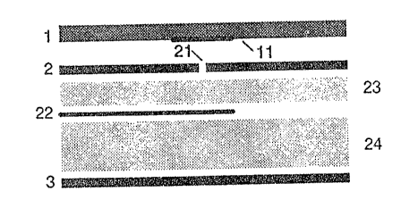
l5 invantion~ Fiqu~~ 1 illustrates a planar antenna which
oQmpria~a four el~mentaa a bac~sp~,ats l, a metal layer
2, etr3p conductor network 22 arid a baaepla~ts 3. The
bsa~p~.aLa 1 is praPerably made of glees ar a fib~rr
coarpoaits, on which radiation sl~art~n~ts 1.1 may be vaouuzn
aU c~~pc~eitad or appliod by a printing process as inw~rtsd
radiating antenna elements. planar radiation slam~ntg
11 of this kind axe also cal~.sd patches.
In the atate-of-ths~.art arrangement deaaribed in
they above-reforeno~d artioln in ~lect,g~g~netics,
2~ Yolume 9, 1989, pa.gsa 3~5~393, there is a foam ins~rt
behind these inverted radiation ~aatchss. It, has bgsn
found, ho~rev~r, that surface crave propagation does not
occur to thm extant exp~eGt~d, ~rhich enables this lay~~r
to ba omitted. If this lmyex ia~ omitted, the follos~ing
30 slot radiating layex c~tn ba po~itianed aloe~r to xhe
plmne~ of the inverted radiat3,ng patches.
In Contra~t, th~ pr~asen~: Claim~d invention
provides a foam layax 23 betcassaz~ the metal layex ,~ with
radiation op~rainc~a 21 and s~txip conductor network 22 on
3g one aide, and a foam layer 24 b~at~regn the latter axed a
5
baseplata 3. ~a~~ap~,ato 3 ac~ns9.~te ~f metal ar of a
~.sayer of metal deposited on a base, rr~ addition,
polystyrene, polypropylene, ar pelxa~m~.d~s are eu~.tabl~a
as foamed materials.
xn any ~~runtr th6 foam layer moat posmese both low
d~nsity and a I~aw relative peg°mittivl.ty.
In a prefarr~sd embodiment, the two foam lnyexw .'23
and 2~ are not of equal this%naes. Also acaorc~ing to a
preferred embodiment, th~ ~tt~.inr~~r of th~ t~ao, laysx 23,
ie mounted on the coupling s3.de and the thicker, layex
2~, is mounted hetwe~st the strip conductor network 2a3
and the baaeplats 3.
As showaa iri Figure 1, ono side of the carrier
elate 1 seals off the envirasu~gnt. ~n its inner
aurfaae, the a~arri~ar plate has electriaal~~,y conductive
patches 11, which, as is t4 be s~on fram figure 2, may
be s~qut~ra in aht~p~a, for exaritgle, and be a~paasd at
regular fnt~xvala from ~sch ~th~r. these ~leatriaally
aonduativ~ patches can ba any suitable material, such
ag a suitable conductive metal., anclz~ay be applied in
any suitable m~ex~nex, such as being vapn~ dm~poeitgd,
laminated, or print~d. ~ppoeita each patch 11, the
cotapling netw~~% 2 has a slot-like opening (coupling
~le~t) in the layer of met$l, a~ shown by la'igurg 8.
Layer 2 taste on the foam la~~yer 23. On the xeverse
side of layer 23 i~ i.ocat~d ~a diatribut.ion nmtwork 22,
a$ shown iza Figure 9, by mean~ of ~rhich th~
transmittivity of the cou~rl3ng slot 21 is ceanC~re~Iled.
the leads r~aqu,txed for this puxpose are on th~ revex$e
side of the foamed materrial 23. '~ha baaeplate 3
i prov~.dsa a seal from the env3xonanent, zt ooneiet~ of
' m~9ta1 or is d~esignerd as a m~tallia reflec~Gt~x.
%n a~aordario~s r~ith furt.h~r~c aspects of the
invantian, three additional r~aodifiaationo of the ~~~z~
teohnolagy are utili~e~t whioh, for the moat part,
caratribute tho bandwidth ~znlargement or reduction of
the r~e~l~ct~i~n i'actor. '
~iret, the o~,enin~s 21 ? n the radigti.on g~lat~s 3
ven be H-shaped and butt~xfly-shap~d, ~,~ illustrated by
the ccnfiguratian in Fi.g~x-rg 38 in addition to b~e~.ng in
the loran oaf alot~ .
6eaond, the etub cableu gunder the openinc~~ 21j in
the d3.atributi~r: riat~rork 22 are impedaa~oo ~nntohad. fro
forma ~f 8~ch fully ~aaxchad ~trip conductor netwox~3ce
axe ~ho~z in ~'a.gure d .
Alga, the xe~diat3.~n ele:~ant~ (patches 12j may be
~qua~re, round, r~atangular, or cruse-shaped or aru~y hate
a a~riee of strips of agual or txnet~usl 1~ngth and
varying width . A typical patch in at~cip form is a~ha~rn
in Figure 5. Ths~ 1~ngth of the ~axi,oue ~~agments of ~a
patc7~ ~.~ ad~uated in such a way th~s~. ~aah segmdnt
o~r~.ape a paa~t of the de~ir~ad cluster.
xn contrast to the abave-referenced
~~.ec~~~~.pn~~iG~ publication, the antenna of thc~
presont invention is constructed hawing substxctea no
langer cazaaLating of tef~.oa~ or ea ceram~,o, but are s~ada
~~ le~~ ceratly e~ateriala. ~,ayer 1, ~o~r ~xampl,es,
consists of g~a~.ily da.~posabis~ glass . ~~,a~~ as a ~~sl
against the enviz~anment prey~nto ra great advant~sq~r ire
ttast it ca.a withstand a? 1 harmful envirorunentnl
influences and can easily be cleaned wh~n necea~ary.
~a~ addition, an antonnr~ of xh~.a design could be eaai7ly
and a3.m~rl;y inbec~rated int.a th~r facades pf high-.ri.se
buildings, The coupling natwaxk is mounted betwe~n
~~D fmamed mntaxial and air, and in this ~.natanc~, is he7ld
in poeit$.on xelc~tiva t~ lay~r 1 by spacers .
The antenna gay b:~ assembled with cane or more
m~.emeri't~ ~pwtches j . 9evmral e~.emarl~e may be arranged
either ia~ g calumn or aide by aid~.
7
the auston2axy vQrtioal radiation pattern ae
illuatra~~d in Figure ~ exhibits di~tinot Faro settings
91 between the Individual beams 44, ~~. controlling
the coupling slots 21 by means of the distribution
network 22 ~llowa uniform ill~minat3ors of the area to
be irrad.tated. In the examples disaueESed in th~
Foregoing, it has been oustomar~r with th~
~tate-of~Ghemaxt eguipment fox the di~:eotiori of maximum
radiation to be positioned pexpendiou5.ar to the plane
of the antenna, so that this antenna plane has had to
be mount~d obliquely fox illuminations as shown in
Figure 5.
~h~ antenna de~ign of the present invention ria~
~akag it possible to orient the dir~ction of maximum
radiation in a limitod range, fxvm the elsctrical
viewpoint at any rate, eo that the plane of the antenna
can be mounted independently of the direCtiori o~
maximum radiation, as is oleaxly s~~n fram Figur~~ 6.
xn addition to the suitably shapod mayor lobe ~4 as
ahoarn in Figuxe 7, a side lobe ~3, for example, can b~
directed and amplify~d in suoh a way that an area so
rote as not to b~ irradiated by the mayor lobe A4 oan
be illuminated. Iri addition to generation of an
optimised vertical radiation pattern, generation of the
~5 horisontal beam direction at any desir~d angle of
approximat~ly t 30° to the vex~.ical of the plane of i~he
antenna is possible. ~ir4ilarly, more than one
arbitrary dixoction of rad.~at.ion is also possible in
the horizontal plane,
Tn the poet, it has been possible to build
antennae measuring up to about only 30 om by 30 am as a
result of aoristraints imposed by coats, teahnaloc~r, and
the manutaaturing,process. ~oCArding to the present
invention, antennae can b~ built which are suitable for
3g reception by way of satellites Eor mu~ic broadcasting,
~0~~~~~
flat antennae ~ to 4 Gm ~hie~s and d~ almoot any dagired
visa. ~ha only as~na~raints imposed axe represented
firatlx by the gla~s area that can he ob~a,ined, and
secondly, by the area that aan ba printed by ecxean
printing.
gn the exaraplp shown i,ri ~ig~ra a, th~ patches ar~
dxa~rt as a~uaxe~, g~ i~ Vbvinua ~o any a~per~P
howevex, that other geometric ahapeg era paasible as
patches, as far a~ampla circular ar~ae, ellipses or
1Q raCtanglea, or parallel ~tripa.