Note: Descriptions are shown in the official language in which they were submitted.
ng-go-oo~ 2 ~ Q
AN APPARATUS AND A METHOD FOR
AN OPTICAL FIBER INTERFACE
FIELD OF TIIE INVENTION
The present invention relates generally to a new interface and a method for making the
same, and more particularly, to an optical fiber interface and a method for making the same. On a
substrate having semiconductors, a receiver/transmitter connection is provided to interface with
an optical fiber. Integral means for the fiber alignment, support and transit through a sealed
environment is also provided. The substrate having the receiver/transmitter secured to it with the
optical fiber end, is then enclosed in a housing.
BACKGROUND O-F THE INVENTION
Optical fiber interconnection for computer communication applications such as clock
distribution, memory and interprocessor data bus, matrix or cross-point switches offer a unique
set of advantages in system architecture, package design, function, and pe~rol~ance. On the
other hand there are some problems associated with this technology.
One of the problems is in the assembly and manufacturability of optical fiber links for
interconnection, such as, tolerances on fiber alignment to the semiconductor junctions of the
optoelectronic communication devices, viz. Iaser transmitters and photoreceivers. Arrays of fiber
links into fluid-sealed semiconductor chip packages further pose problems in strain-relief at device
interfaces, fan-out distribution,
FI9-90-001 2 2 ~ ~12 9 ~
.. integrabi~ity, and spatial efficiency. Some of these
known problems have been resolved by this invention.
The application of preferential crystallographic
etching of V-grooves in silicon with photolithographic
accuracy was taught by Crow et al., "GaAs Laser Array
Source Package," OPTICS LETTERS, Vol. 1, No. 1, pages
40-42 (July 1977). His work also established the
feasibility of achieving the required fiber core
alignment tolerances.
U. S. Patent 4,730,198 (Brown, et al.) extends the
application of V-groove fiber mounting techniques, which
were compatible for electrical and optical connections.
Optimi2ing emitter (LED or ]aser diode) placement
relative to a fiber-optic silicon V-groove was treated by
Balliet et al., in IBM Technical Disclosure Bulletin,
Vol. 24, No. 2, pages 1158-1160 (July 1981), by balancing
the outputs of a pair of junction diodes integrated on
the undersides of the V-groove.
Methodology for preferential chemical etching of
GaAs is given in Commerford and Zory, "Selectively Etched
Diffraction Gratings in GaAs," APPLIED PHYSICS L~TTERS,
Vol. 25, No. 4, pages 208-210 (August 15, 1974), and
Tsang and Wang, "Profile and Groove-Depth Control in GaAs
Diffraction Gratings Fabricated by Preferential Chemical
Etching in H2S04-H202-H20 System" APPLIED PHYSICS
LETTERS, Vol. 28, No. 1, pages 44-46 (January 1976).
Extension of fiber V-groove structure to GaAs
~ substrates with self-aligned monolitllically integrated
--' GaAlAs laser was shown by Brady et al., in IBM Technical
Disclosure Bulletin, Vol. 26~ No. 11, pages 5993-5995
(April 1984) to provide submicron photolithographic
alignment tolerances.
Thus, it is clearly recognized that either silicon
or gallium arsenide V-grooves may be used.
In U. S. Patent 4,732,446, (Gipson et al.) optical
fibers were embedded within the body of a printed circuit
board and interfaced with discrete, lense~ and beam-split
chip carriers to create a simultaneous optical bus and
electrical data network. Multiple printed circuit board
layers, separated by aluminum heat sink plates, could be
20~12~
FI9-90-001 3
stacked and a card edge connector could form the
interface to incoming data cables. Because of the
multiplicity of chip carrier interfaces the modal noise
and optical power losses associated with this structure
can be expected to significantly exceed those of the
present invention.
Conventional approaches for electrical connection
include the wire bond lead or "T0-# Can" package typified
in U. S. Patent 4,647,148 (Katagiri) and, "tab
connection" typified in U. S. Patent 4,722,586, (Dodson
et al.).
The present invention teaches compatible designs for
interfacing external lightwave conduits into a
fluid-sealed, temperature-controlled module, and, direct
distribution within the module to selectable
semiconductor chip positions, in either simplex or duplex
fiber modes, for either bidirectional or unidirectional
lightwave signals. The present invention further teaches
direct surface connection, avoiding passage through
module layers or cooling structures, and, eliminating
auxiliary arrays of photonic transmitters and receivers
at the module-cable edge interface, as disclosed in U. S.
Patent 4,169,001, (Kaiser).
The use of controlled collapse chip connection (C-4)
with lithographically precise solder ball arrays for
positioning and electrically connecting the optical
pedestal to the substrate having semiconductors further
distinguishes the present invention.
In the present invention, the optical pedestal and
C-4 provides an integrated optical subassembly and
alignment means, assuring thermal coefficient of
-~ expansion match to the substrate, optimum impedance,
-- spatial efficiency, and reliability. The option for
direct C-4 attachment to the substrate is provided for in
alternate embodiments.
Further mechanical design distinctions of the
present invention include the Thermal Conduction Module
(TCM) - fiber optic penetration assembly, fiber guide
structure, optical fiber strain-relief, optical pedestal
assembly, and separability of the upper and lower
~x
' - ~
FI9-90-001 4 2~2~9
i
half-planes of the TCM, primarily for test and repairs.
OBJECTS AN~ SUMMARY OF THE INVENTION
An object of this invention is to provide one or
more optical fiber links into a TCM.
Another object of this invention is to remove a
decoupling capacitor and utilize its space for an optical
pedestal.
Another object of this invention is to provide means
in a TCM to guide and align the optical fibers to the
optical pedestal.
Still another object of this invention is to provide
means for strain-relief of the optical fiber connection.
Yet another object of this invention is to provide
optoelectronic conversion at the substrate.
- Still another object of this lnvention is to
communicate with semiconductor chips on a multilayered
substrate using optical fibers through a TCM.
Still another object of this invention is to provide
a fluid tight seal for the optical fiber that is
compatible with the present TCM seal system.
Yet another object of this invention provides for
separability in the lightwave signal path for repairs or
test.
Still another object of this invention is to have
the substrate with the chip and the optical pedestal
secured to a portion of the TCM, so that individual
portions of the TCM can be independently separated for
repairs, test, or upgrade.
Yet another object of this invention is to maintain
compatibility with the TCM elements.
Still yet another object of this invention is to
provide means for:
a) penetrating the controlled environment of the
TCM (Thermal Conduction Module) with one or more optical
fibers;
b) aligning and securing the optical fiber through
a guide groove;
c) location and alignment of the optical fiber
ends to receiver, transmitter, or both;
.
-
2 ~ ~
FI9-90-001 5
d) mounting of receiver and/or transmitter devices
on the substrate of the TCM; and,
e) effecting a separable interface between the
fiber and the receiver or transmitter devices.
One aspect of this invention discloses an apparatus
for optical fiber interface comprising:
a) a substrate,
b) at least one optical receiver on at least one
surface of the substrate~
c) at least a portion of at ]east one optical fiber
optically communicating with the at least one optical
receiver,
d) a housing protecting the at least one optical
receiver and the substrate, and
e) means in the housing for communicating an
optical signal through the housing to the at least one
-- optical receiver via the at least one optical fiber.
In another aspect this invention discloses an
apparatus for optical fiber interface comprising:
a) a substrate,
b) at least one optical receiver on at least one
surface of the substrate,
c) at least one optical fiber,
, d) means for guiding the at least one optical fiber
to the site of the at least one optical receiver,
e) means for aligning and securing the at least one
optical fiber to the at least one optical receiver,
f) a housing protecting the at least one optical
receiver and the substrate, and
g) means in the housing for communicating an
optical signal through the housing to the at least one
optical receiver via said at least one optical fiber.
Still another aspect of this invention discloses
a method for providing an optical fiber interface
comprising:
a) securing at least one optical receiver on at
least one surface of a substrate,
b) securing at least one optical fiber to the at
least one optical receiver,
~ '~
~ : ':
-
20~2~
FI9-90-001 6
c) providing a housing to protect the at least one
optical receiver and the substrate, and
d) providing means in the housing for communicating
an optical signal through the housing to the at least one
optical receiver via the at least one optical fiber.
Yet another aspect of this invention discloses a
method for providing an optical fiber interface
comprising:
a) securing at least one optical receiver on at
least one surface of a substrate,
b) providing means for guiding at least one optical
fiber to the site of the at least one optical receiver,
c) providing means for aligning and securing the at
least one optical fiber to the at least one optical
receiver,
d) providing a housinq to protect the at least one
optical receiver and the substrate, and
e) providing means in the housing for communicating
an optical signal through the housing to the at least one
optical receiver via the at least one optical fiber.
BRIEE DESCRIPTION OF '1~ DRAWINGS
The features of the invention believed to be novel
and the e]ements characteristic of the invention are set
forth with particularity in the appended claims. The
figures are for illustration purposes only and are not
drawn to scale. The invention itself, however, both as
to organi~ation and method of operation, may best be
understood by reference to the detailed description which
follows taken in conjunction with the accompanying
drawings in which:
Figure 1 is a cut-away perspective view of an
optical fiber mounting assembly of this invention
interfacing with a TCM.
Figure 2 is an exploded view of the elements of the
optical fiber mounting assembly interfacing with the seal
frame.
Figure 3 is an enlarged cross-sectional view of the
assembled interfacing between the optical fiber mounting
assembly and the TCM elements.
-
20~1293
FI9-90-001 7
Figure 4 is a partial cross-sectional view showing
the passage of the optical fiber through the optical
fiber mounting assembly to the optical fiber pedestal
assembLy.
Figure 5 is an exploded side view showing the
retainer h~ving optical fiber guide grooves, and other
related elements.
Figure 6 illustrates a seal frame having modified
retainer and alignment means.
Figure 7 is an enlarged view of the optical pedestal
--~ assembly on a substrate with the partial guide elements.
~ Figure 8 is a perspective exploded view of the
optical fiber pedestal assembly and related elements.
DETAILED DESCRIPTION OF THE INVENTION
The novel apparatus and method for the optical fiber
interface of this invention is comprised of many aspects.
The primary aspect of this invention is the utilization
of the substrate surface for optoelectronic communication
with little or no effect to other electronic devices that
may be on the substrate. Similarly. the invention allows
for the modification of the cooling configuration of a
TCM with little or no impact to the cooling capabilities
of the TCM. These and other unique features of this
invention are discussed later in this section.
An electronic device as used herein could include
passive circuit elements, such as resistors, capacitors,
and inductors, or semiconductor devices, and associated
circuitry, such as diodes, transistors, logic circuits,
to name a few.
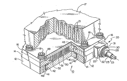
Illustrated in FIG. 1, is a Thermal Conduction
Module or TCM lO, comprising a lower frame 12, an upper
frame 16, sandwiching a seal frame 14, which has been
modified. The lower frame 12, seal frame 14, and upper
frame or hat 16, are held together by securing means,
such as bolts 18. Usually a cold plate 17, having a
number of coolant channels 21, is secured to the upper
surface of the upper frame 16, by means well known in the
art. A substrate 40, having stepped edge 42, and having
semiconductor chips 50, thereon, is secured between the
20~1299
FI9-90-001 8
ledge 41, of the lower frame 12, and the extension of
seal frame 14, with a gasket 46, therebetween. It is
customary to have heat exchange elements 52, such as the
High Conduction Cooling (HCC) elements as disclosed in
European Application No. 8948006~.8, published November
29, 1989 (Horvath, et al.), to transfer the heat
generated ~y the chip 50, to the upper frame or hat 16.
For the purposes of illustration only, the upper frame or
hat 16, is discussed in conjunction with heat exchange
. element 52, or HCC 52, but the upper frame could have any
type of a heat exchange element or cooling device or
structure, for example, the upper frame 16, could be
similar to the one as disclosed in U. S. Patent No.
4,226,281, or the one disclosed in U. S. Patent No.
4,235,283. Of course, in any situation the upper frame
16, would have to be modified to accommodate a guide or a
retainer like element. A retainer 51, holds the heat
exchange elements 52, in place. As discussed later in
this section, this retainer 51, is also used to provide
the guide grooves and securing means for an optical fiber
23. In cooling devices or structures where there is no
retainer 51, the cooling device or structure could be
easily modified by a person skilled in the art to provide
means for guiding and securing the optical fiber 23, from
the exterior of the TCM 10, to an optoelectronic device
on the substrate 40. A fluid tight seal for the chips
50, that are on the substrate 40, may be achieved by
means of gaskets 46 and 48. An optical fiber mounting
assembly 20, provides the interface between the
multi-fiber optical cable 25, and the TCM 10. Face plate
22, keeper 32, wave washer 31, retainer 30, and shoulder
28, are various components of the optical fiber mounting
assembly 20, that normally protrude out of the TCM lO.
The optical fiber mounting assembly 20, may be
located between any adjacent pair of bolts 18, along the
sides of the TCM 10. Therefore, any side of the TCM 10,
may then accommodate (N-l) optical fiber mounting
assemblies 20, where N = number of bolts along the given
side of the TCM 10. Each optical fiber mounting assembly
20, can have a multi-fiber optical cable 25, having one
i : '~
.. ! ,. ,~
_
2061~99
FI9-90-001 9
or more optical fibers 23. Each optical fiber 23,
typically has a core of a first refractive index material
with a cladding of a second refractive index material and
a protective jacket which is typically of a polymeric
material.
FIG. 2 illustrates an exploded view of the elements
of the optical fiber mounting assembly 20, which provides
for optical fiber penetration through the side of the
seal frame 14. The multi-fiber optical cable 25, is
shown with a segment stripped to expose a suitable length
of the clad optical fiber 23. A portion of the clad
segment of the optical fiber is metallized in two places
37, and 77. The distance between the two metallized
locations 37 and 77, is predetermined so as to permit
stress relief after assembly to the retainer 51, and the
seal frame 14. This metallization at locations 37 and
77, is done primarily to securely attach or bond at least
a portion of the optical fiber to a component of the
optical fiber mounting assembly 20, and a V-groove in a
V-block, respectively. The seal frame 14, has a series
of holes 19, to accommodate the bolts 18. A stress
relief sleeve 24, has shoulders 26 and 28, at each end,
and also radial grooves 27 and 29, to accommodate
retaining rings 47 and 30, respectively. The optical
fiber mounting assembly 20, can be prepared by feeding
the optical fiber 23, through the opening in the stress
relief sleeve 24. The metallized segment 37, of the
optical fiber 23, is soldered to a ferrule 39. The
ferrule 39, in turn, at this point could be soldered to
the shoulder 26, of the stress relief sleeve 24. This
sub-asse~bly can now be fed through the hole 9, in the
seal frame 14, and the face plate 22. The retainer ring
47, is expanded and then relaxed into the groove 27. The
stress relief sleeve 24, is now pulled away or back from
the seal frame 14, and O-ring 33, keeper 32, wave washer
31 and retainer ring 30, are slid in place to fully
secure the stress relief sleeve 24, to the seal frame 14.
This is accomplished by relaxing the retainer ring 30,
into the radial groove 29~ which compresses and securely
holds this assembly in place against the face plate 22.
- ~
2~612~9
FI9-90-001 10
The retainer ring 47, inserted in the radial groove 27~
at the other end of the stress relief sleeve 24, securely
locks the stress relief sleeve 24, in place on the inside
of the seal frame 14.
A V-block 70, having channel interlock 96, can now
be soldered to the metallized segment 77, that is at the
end of the optical fiber 23, as shown in FIG. 3. The
external end of the jacketed multi-fiber optical cable
25, may no~ be stripped and an appropriate fiber optic
connector can be attached. FIG. 3, further shows an
enlarged cross-sectional view of the assembled optical
fiber mounting assembly 20, as part of the seal frame 14,
and the upper frame 16, and the lower frame 12. The
optical fiber 23, is passed through a stress relief
sleeve 24, so that a ferrule 39, may be secured at this
time to the metallized region 37, on the clad optical
fiber 23, by suitable means, such as brazing, laser
welding, or soldering, to name a few. The ferrule 39, is
positioned so that it is flush with the face of the
shoulder 26, at the end of the stress relief sleeve 24.
The ferrule 39, can now be secured by any suitable means,
such as brazing, laser welding, soldering, etc. to the
end of the stress relief sleeve 24. Similarly, the
metallized end 77, of the clad optical fiber 23, can be
secured to a preferentially etched, metallized groove in
the V-block 70, by suitable means, such as brazing, epoxy
bonding, laser welding, or soldering to name a few. The
V-block 70 may have one or more V-grooves, as discussed
later in this section, that are preferentially etched on
its underside depending on whether it is a simplex or
duplex application. The V-block 70, with optical fiber
23, secured thereto is placed in a holding tool and
ground and polished to produce an appropriate angle for
internal reflection of light waves on the end face 98, of
the optical fiber/V-block assembly 70. The angled facet
of the V-block 70, and the end face of the optical fiber
23, is so devised to reflect optically transmitted light
, waves downward. The ground and polished end face of the
optical fiber/V-block assembly can be metallized as
required. The lower frame 12, and the upper frame 16,
-
2061~99
FI9-90-001 11
are sealed with gaskets 46 and 48, respectively. The
gasket 33, provides an effective seal for the optical
fiber mounting assembly 20. These gaskets 46 and 48, can
be an "0-Ring" or a "C-Ring", type gasket to effect
sealing when assembled to other elements of the TCM 10
using bolts 18. A pad 43, that is between the ledge 41,
and stepped edge 42, provides a cushion for the substrate
...... . ..
40.
FIG. 4, illustrates a partial cross-sectional view
showing the passage of the optical fiber 23, through the
optical ~iber mounting assembly 20, to the optical fiber
pedestal assembly 150. This optical fiber pedestal
assembly 150, can be placed practically at any location
on the substrate 40. These locations could include the
sites for semiconductor chip 50, or the sites for
decoupling capacitor 74, or between chip edges or
piggyback on a semiconductor chip 50, to name a few. The
preferred location is to replace a decoupling capacitor
74, with an optical fiber pedestal assembly 150, because
by removing a few decoupling capacitors 74, there will be
negligible loss in noise immunity, but the removal of a
semiconductor chip 50, could have significant loss in
circuit capacity. Additionally, this replacement can be
done with minimal design change of the substrate wiring.
This introduction of these lightwave communication
devices provides a significant increase in functional
densities and communication data rate.
The thermal expansion differential of the various
materials in the TCM wil] produce strain on the clad
fiber 23. This expansivity differential between the
optical fiber 23, and the TCM 10, can be accommodated by
allowing a portion of the optical fiber 23, to arch
inside the housing of the TCM 10, to provide strain
relief. This is accomplished by letting the distance
between the optical fiber pedestal assembly 150, and the
internal optical fiber exit point of the optical fiber
mounting assembly 20, be the chordal distance subtended
by an arc formed by the optical fiber 23, as shown in
FIG. 4. The optical fiber 23, is predisposed to forming
this arc, and this can be achieved by having the length
~0612~
FI9-90-001 12
of the optical fiber 23, be greater than the chordal
distance. In this manner, any differential length can be
transformed into a longer or shorter arc length for the
optical fiber 23. The arc length variability is
translated to flexure stress in the optical fiber 23,
which provides strain relief at the fiber V-block 70.
- The external optical fiber connector should preferably be
of a kind that provides strain relief. The retainer 51,
has openings 66 and 67, to accommodate the optical fiber
pedestal assembly 150, and decoupling capacitor 74,
respectively.
It was also discovered that the existing cooling
configuration of part of the upper frame could be
modified to allow containment, passage and alignment for
the optical fiber and the V-block assembly. This
modification allows for maximum utilization of the
cooling configuration without impacting the cooling
performance. For the purposes of illustration only, the
cooling configuration of European Application No.
89480064.8, published November 29, 1989 (Horvath, et al.)
is shown in FIGS. 1 and 5, but any existing cooling
configuration can be similarly adapted to be used with
this invention.
In order to position the optical fibers 23, within
the available space in the TCM 10, the retainer 51, and
' the upper frame 16, are modified. Some of these
- ~~ modifications are shown in Figure 5. The retainer seat
53, is modified to accommodate the retainer 51. The
retainer 51, must also be modified to provide means for
securely holding at least a portion of the V-block 70.
~ The upper frame 16, is also modified by shortening one of
the retaining guides or large fins 56, to form a stub
guide 58. The stub guide 58, has a restraining groove
59, to accommodate the key 57, which is part of the fiber
guide 69. The periphery of the upper frame 16, has a
groove to accommodate gasket 48. The fins 54, on the
upper frame 16, mesh with the fins of the HCC 52, as
described in European Application No. 89480064.8,
published November 29, 1989 (Horvath, et al.). The
retainer 51, is a standard retainer that is used in
. . ~ ~ ~ ... .
20612~9
t FI9-90-001 13
:
conjunction with the upper frame 16, but now has been
modified to have at least one fiber guide 69, having
tapered channel 55, and key 57. The retainer 51, also
has at least one boss 63, with an opening 65, to
accommodate an eccentric pin 64. The HCC spring 62, is
normally inserted in the openings in the HCC 52, and this
sub-assembly is then placed in the openings in the upper
frame 16. The retainer 51, and the retainer spring 60,
are then securely attached to the upper frame 16, with
the seal frame 14, securely holding this assembly in
place. The retainer spring 60, has openings (not shown)
to allow the passage of the upper surface of the fiber
guide 69, and the key 57, that mates with the restraining
groove 59. The result of this modification is to provide
a fiber guide channel 69, and still effect the X, Y and
Z-axis movement control for the heat exchange element or
HCC 52. The clad optical fiber 23, is placed in the
tapered channel 55, and the V-block 70, is inserted into
the slot provided for it. The tapered ridge 96, on top
of the V-block 70, matches the walls of the retainer
channel 55, and hence provides self-centering of the
V-block 70, with the tapered channel 55. With the
V-block 70, so positioned, a spring clip 61, having an
aperture so as to permit passage of optical lightwaves is
placed around the V-block 70, to capture it. The flat
spring 60, that is placed between the retainer 51, and
the upper frame 16, maintains engagement between the
V-block 70, and the receiver chip 80, during normal
operation through the fiber guide 69, and precludes
Z-axis motion and compensates for substrate 40,
deflections due to module connector actuation, or other
forces that might deflect the substrate 40.
The retainer 51, having sector rib 68, to position
HCC 52, is assembled through the top of the seal frame
14, by using two of its adjacent edges to compress a bias
spring 101, located in the inside wall of the seal frame
14, as illustrated in FIG. 6. Corresponding bosses 121,
to bosses 63, on adjacent edges of the retainer 51, are
located on the inner sides of the seal frame 14. Bias
spring lOl, is located on the inner sides of the seal
2~2~
FI9-90-001 14
frame 14, to force the retainer 51, against eccentric
pins 64, located on the bosses 121. The adjacent edqes
of retainer 51, are made to compress bias spring 101, so
that openings 65, then engage eccentric pins 64. By
rotating either eccentric pin 64, the retainer 51, can be
precisely positioned in the X and Y axis. An interlock
key 49, secures the retainer spring 60, that resides in
opening 104. When the various components of the TCM 10
such as lower frame 12, seal frame 14, upper frame 16,
optical fiber mounting assembly 20, are assembled, care
should be taken that these components provide a fluid
tight seal, as the electrooptic components and other
electronic devices on substrate 40, must be protected
from outside environmental elements. Also, in some
cases, the TCM 10, may contain a fluidic medium that acts
as the cooling or heat transfer medium for the various
electrical and optical components that are on the
substrate 40. The stress relief sleeve 24, can also be
modified to accommodate any number of optical fiber
connectors. One such connector is shown as optical fiber
connector 99. Use of such an optical fiber connector 99,
would make the TCM 10, modular or be plug-compatible.
Figure 7 is an enlarged view of the optical
pedestal assembly 150, with the partial guide elements
positioned on the substrate 40. The channel interlock
96, on the V-block 70, is inserted in a precisely located
slot in the guide channel 69, and retained by a spring
clip 61. The spring clip 61, has an aperture on its
underside to permit free passage of light wave
transmission from or to the angled optical fiber ends 97
and 98, to the receiver chip 80, and the coupling lens
88. The optical input/output can further be processed
through a laser chip 90, laser driver 91, and the
i function generator chip 92. A ~stand-off 75, electrically
~ isolates the receiver chip 80, from the electrical
surface contacts on the optical pedestal 76. Tabs 81,
contact the receiver chip 80, to the optical pedestal 76,
through contact pads 112. Similarly, printed circuit
lines 78, electrically connect the optical pedestal 76,
to the optical transmitter carrier 86, through tabs 94.
2~612~9
FI9-90-001 15
,, . . , .,~ . ~ ~
The substrate 40, has solder pads 72, for mating with the
solder balls 102, on the bottom of chip 50, or the
optical fiber pedestal assembly 150, or the decoupling
capacitor 74, not shown. The sector rib 68, is used to
position the heat exchange elements 52, not shown. The
retainer 51, has a key 57, and an optical fiber guide 69,
that contains the tapered channel 55, as shown and
discussed in FIG. 5. The key 57, has openings 104, to
accommodate spring clip 61, and the flat retainer spring
60, using the interlock key 49.
The optical fiber pedestal assembly 150, is shown
bonded to a substrate 40, in FIG. 7, and is discussed in
detail in FIG. 8. The substrate 40, can be a
multilayered ceramic (MLC) substrate 110. The substrates
40 or 110, normally have solder pads 72, to mate with the
solder balls 102, that are on the underside of the chip
50, or the optical pedestal 76, or the decoupling
capacitor 74 (not shown).
FIG. 8, shows an exploded view of the optical fiber
pedestal assembly 150, and its related elements. The
optical pedestal 76, is preferably positioned along the
fiber guide channel axis and between any pair of bolts
18, as discussed earlier. As discussed herein optical
fiber 125, couples to a detector 100, on the receiver
chip 80, and optical fiber 123, communicates with the
laser chip 90, through the coupling lens 88. However, a
single optical fiber can be adapted for bi-directional
optical communication with the receiver chip 80, and the
transmitter carrier 86. The optical pedestal 76, is a
multilayer ceramic having a pattern of solder balls 102
on the underside for effecting a controlled collapse bond
to a similar array of solder pads 72, which is shown
configured on the surface of a multilayered ceramic
substrate 110. The MLC optical pedestal 76, provides for
electrical connection between the optical pedestal 76,
and the MLC substrate llO, and is in optical contact with
at least a portion of the optical fibers 23 or 125,
through the receiver chip 80. The multilayered substrate
llO, typically has pins ll~, on the underside, which are
electrically connected to metal layers 114, by means of
.
''',~ -
FI9-90-001 16 20S~2~
metal filled vias 116. This electrical path provides
electrical connection to external circuitry and power
_ distribution.
- Printed circuit member 84, is bonded to one side of
the optical pedestal 76, to provide contact pads 112 for
attaching tabs 81. Similarly, the printed circuit member
93, having tabs 85, is attached to the other side of the
optical pedestal -76, to provide the pads to mount tabs
183. Tabs 82, along the upper edge of printed circuit
member 84, are formed so as to allow bonding to the pads
73, on the optical pedestal 76. A projection or
stand-off 75, is preferably located centrally on the top
surface of the optical pedestal 76, to which the receiver
chip 80, is bonded so as to preclude contact of the
receiver chip 80 and the tabs 82 and 85.
The V-block 70, could have a plurality of V-grooves
95, to accommodate a plurality of optical fibers 23, 123
or 125, as well as provide for V-block retention. The
V-grooves 95, etched in the V-block 70, may be defined
lithographically in either GaAs or Si. The V-grooves 95,
that are used to accommodate one end of the optical fiber
23, can be, for example, etched in (100) silicon with
either ethylenediamene or KOH solutions. See for
example, E. Bassous, "Fabrication of Novel
Three-Dimensional Microstructllres by the Anisotropic
Etching of (100) and (110) Silicon" IEEE Transactions on
Electron Devices, Vol. ED25, No. 10, pages 1178-1185
(October 1978). Because of the nature of anisotropic
etching, a definition of the width of the channel also
defines its depth by simple geometry, in order to place
an optical fiber 23, or 123 and 125, into V-grooves 95,
so that the optical fiber 23, or 123 and 125, are tangent
to the V-groove walls at points enabling the optical
fiber axis to be coplanar with the surface of the
silicon. With accurate control of temperature and time,
-etched V-grooves can be defined with great accuracy. The
material for the V-block 70l is preferably selected from
a group consisting of germanium~ silicon, binary alloys
of gallium or indium with arsenic or phosphorus, and
- ternary alloys of aluminum with gallium or indium with
-
FI9-90-001 17 2 0 ~12 ~ 9
arsenic or phosphorus. Typical materials are silicon,
germanium, gallium arsenide, indium phosphide, etc.
At least one of the V-blocks 70, could have means to
align and secure it to a complementary aligning and
securing means in the receiver chip 80. This could be
done very easily by either having a male/female on the
V-block 70, that mates with a female/male portion on the
receiver chip 80. Another way of providing this
alignment could be etching at least one dummy V-groove in
the receiver chip 80, and securing at least one
cylindrical key, such as a dummy optical fiber, into one
of the V-grooves 95, and then aligning the V-block 70,
with the cylindrical key such that the cylindrical key or
dummy optical fiber gets secured into one of the dummy
V-grooves on the receiver chip 80. Additionally, an X-Y
alignment lock can be created by preferentially etching a
second V-g.oove that is preferably transverse to the
first V-groove into the receiver chip 80, and thereby an
- X-Y alignment lock can be formed. In this case the
V-block 70, will have to have at least two cylindrical
keys, so that each one goes into each of the
corresponding etched grooves.
The optical fiber 23, or 123 and 125, are secured
into the V-groove g5, by any suitable means, such as
brazing, laser welding, soldering, epoxy bonding, etc.
The outside surfaces of both the optical fiber 23, or 123
and 125, and the V-groove 95, are prepared for further
joining, such as by metallizing with successive layers of
appropriate metals which are vacuum deposited. If solder
i3 to be used, then the optical fiber 23, or 123 and 125,
are bonded into the V-grooves 95, with eutectic ~older.
The solder can be applied either by vacuum deposition or
by use of solder preforms. It is important to keep the
optical fiber 23, or 123 and 125, in the V-groove 95,
during the bonding or securing operation. This can be
done with a simple jig wherein a plate is pushed against
the optical fiber 23, or 123 and 125, to keep it in the
V-groove 95.
To permit the light cone to exit the optical fibers
- 23~ or 123 and 125, at a cone axis of 90-degrees to the
,
20~i2S9
FI9-90-001 18
optical fiber axis, the end of the optical fibers 23, 123
and 125, may be cut at an angle (beveled). This can be
accomplished by a simple grinding operation with the
optical fiber bonded to the V-block 70. The resulting
optical fiber end face is then metallized for reflection,
or the bevel can be made so as to cause total internal
reflection where no metallization is required. One can
also use a beam-splitter for bi-directional lightwave
transmission.
The V-blocks 70, can be batch fabricated. This can
be done by configuring V-blocks 70, on a silicon or
gallium arsenide wafer as a cell array. Each cell
boundary is defined by etching a V-groove contiguous with
the desired four sides of the V-block 70. The desired
number of V-grooves 95, for attaching the ends of optical
fibers 1~3 and 125, are etched simultaneously with the
V-groove defining the cell boundary. Using conventional
photolitho~raphic processing, the wafer is photoresist
coated, exposed through a blockout mask, developed,
metallized, and, finally, stripped to selectively open
suitable optical fiber bonding surfaces in the V-grooves
of each cell. The V-blocks 70, are now diced out of the
wafer in strips by cleaving along the cell boundaries
that had been etched ear].ier and these boundaries are now
transverse to the strip of the optical fiber V-grooves
95. The metallized fiber ends 123 or 125, are bonded to
the appropriate V-grooves of each cell in a strip. Each
strip is then fixt~lred and groulld to produce angled fiber
end faces 97 or 98. These strips that are in a bar form
are then finally diced into individual V-blocks 70, by
further cleaving along the etched cell boundaries
parallel to the V-grooves 95.
Cleaving along the parallel cell boundaries results
in etched, tapered V-block sidewalls 1~6, as shown in
FIG. 8. These tapered V-block sidewalls 126, are used to
retain the V-block 70, in the .slot of the optical fiber
guide 69, with spring clip 61, shown in FIG. 7. Spring
clip 61, should have a matching taper for retaining the
V-block 70, so that the fiber can be placed flush with
the receiver chip 80. These tapered V-block sidewalls
2 ~ 9
FI9-90-001 19
126, retention means eliminate mechanical interference
between spring clip 61, and the receiver chip 80. The
ability to flush mount the optical fibers 123, 125 to the
receiver chip 80, eliminates the need for a coupling
lens.
The optical pedestal 76, is extendible to
accommodate an optical transmitter carrier 86, as shown
in Figure 8. A coupling lens 88, such as a GRIN (graded
refractive index) lens can be positioned in the V-groove
of the optical transmission carrier 86, for alignment to
the laser chip 90, located on the optical transmitter
carrier 86. As can be seen by the dashed lines in FIG.
8, that a portion of the optical fiber 123, is in optical
contact with the optical transmitter 86. The optical
transmitter carrier 86, has means for optically
communicating the information received from at least one
of the electronic devices on the substrate 40 or 110, to
one or more of the optical fibers, such as optical fiber
23 or 123. For bi-directional data communication, a
single optical fiber 23, with partial-silvered angled
endface is mounted in V-groove 95, with the transmitter
coupling lens 88, orthogonally aligned to the optical
fiber axis. The finished optical pedestal assembly 150,
is then reflow-bonded on to the substrate 40 or 110, as,
for example, at the vacated corner capacitor 74,
position. Electrical wiring from the optical pedestal
76, to the appropriate chips 50, cotnpletes the circuit to
the optical receive-transmit circuitry.
The optical pedestal 76, may then be simultaneously
reflow soldered to the substrate 40 or 110, along with
7 the semiconductor chips 50. After reflow soldering the
optical pedestal 76, can be selectively reflowed again
in a vacuum aided planarizing and height referencing
tool. This operation positions the optical pedestal 76,
for optimum alignment with the optical fiber 23, or 123
and 125, mounted in the V-groove 95, in the V-block 70.
The optical pedestal 76, llas internal wiring to
connect electrical paths through the C4 or solder pads
72, from the multilayer ceramic substrate 110, to
peripheral pads 73, 79 and 89, on the optical pedestal
2~12
FI9-90-001 20
76. Printed circuit members 84 and 93, are bonded to the
sides of the optical pedestal 76, as discussed earlier.
Tabs 82 and 85, are thermo-compression bonded to the pads
73 and 79, respectively. The receiver chip 80, is then
bonded to the projection or the stand-off 75.
Optionally, the coupling lens 88, is aligned and bonded
to the optical transmitter carrier 86, and this assembly
is then bonded to the optical pedestal 76. Tabs 87 and
94, on the optical transmitter carrier 86, can now be
thermocompression bonded to the pads 89, and the printed
circuit lines 78, respectively, on the optical pedestal
76. Using a vacuum assisted tool the optical pedestal
76, along with the receiver chip 80, and the optical
transmitter carrier 86, secured to it, can be reflowed
against a 3-point reference that in turn is referenced to
a 3-point reference about the perimeter of the MLC
substrate 110. During this reflow process, the C4s or
solder balls 102, may elongate but at no time, will they
be discontinuous. The tool may angularly rotate the
optical pedestal 76, to achieve alignment with reference
marks etched in the thin films of the wiring pattern on
the substrate 110. This alignment is held for a long
enough time to allow the so]der balls 102, to solidify
again.
The seal frame 14, retainer 51, lower frame 12,
substrate 110, and gasket 46, are properly assembled and
compressed to sealing conditions and are optimally
aligned. Similarly, at least a portion of the optical
fiber 23 or 125, must be optically aligned with the
photodetector 100, on the receiver chip 80, After the
optical alignment, the photodetector 100, can be
electrically activated. The optical fiber 23, in a
simplex case, or optical fibers 123 and 125, in a duplex
case, are connected to a test set-up allowing
transmission of optical test patterns. By observing the
output level of the photodetector lOO, the eccentric
threaded pins 64, are rotated to laterally position the
fiber end face for peak signal output. The substrate
110, can also be laterally adjusted to optimize it for
optimum pin/connector alignment and the optical fiber 23,
2~12~
FI9-90-001 21
or 123 and 125, can again be realigned for peak signal
output.
If the lightwave signal input is used for optical
clock distributlon, then only one to five optical fibers
23, may be required. For bi-directional data
transmission 35 to 40 simplex optical fiber pairs may be
used.
Another advantage of this invention is to supply
optical lightwave communication or optical signal for
clock distribution and/or data-bus applications.
Typically an electronic clock distribution system is
comprised of a master oscillator from which a clock pulse
train is distributed to satellite electronic functions,
such as a logic chip on a substrate contained in a TCM.
This invention enables the application of laser clock
generation and optical fiber distribution in a
conventional TCM. Additional advantages of this optical
clock distribution system relative to the present-day
electronic clocking systems include the following:
a) reduced skew (clock pulse arrival time
variation);
b) low noise at high clock frequencies (greater
than 100 MEIz.
c) increased distance between electrical functions
by use of optical fiber;
d) eliminate speed-matching buffers.
If an optical clock were to be utilized such as the
one in this invention, a practica] implementation would
entail the distribution of a clock pulse train to each
quadrant of the MLC substrate. Further clock
distribution by the electrical nets within each quadrant
then synchronizes the logical operations to a machine
cycle-time for the computer chips.
In the data bus applicatioll, high-speed serialized
bits of data must be communicated between memory
locations or between data storage and logic chips. This
invention enables the use o~ optical fibers to connect to
transmitters with suitable encoders, serializer and
link-adapter chips. Furthermore, the use of optical
fiber allows the use of large bandwidths of data to be
2~61299
FI9-90-001 22
communicated between receiver, decoder, deserializer, and
clock-recovery chips at other memory or logic chip
locations within the computer system complex. The use of
optical fiber enables the use of new architectures for
coupling many processors and data storage devices
together for expanded memory and parallel high-speed
operation across optical interconnections between these
communication nodes. Other advantages of optical data
bus interconnect using optical fiber include bandwidth
ability to provide very high I/O through multiplexing in
frequency or wavelength, greater transmission distances
between I/O devices, greater distance between logic and
memory, packaging compactness and light weight relative
to copper cables, and compatibility with future optical
crosspoint switching and data communication on long-haul
telecommunications.
While the present invention has been particularly
described, in conjunction with a specific preferred
embodiment, it is evident that many alternatives,
modifications and variations will be apparent to those
skilled in the art in light of the foregoing description.
It is therefore contemplated that the appended claims
will emLrace any such alternatives, modifications and
variations as falling within the true scope and spirit of
the present invention.