Note: Descriptions are shown in the official language in which they were submitted.
FI9-91-053 1 2 0 6 1 3 2 8
AN APPARATUS AND A METHOD FOR AN
ELECTRICAL TRANSMISSION-LINE INTEREACE
FIELD OF THE INVENTION
The present invention relates generally to a new
interface and a method for making the same, and more
particularly, to an electrical transmission-line
interface and a method for making the same. On a
substrate having semiconductors, a driver or receiver
circuit is provided to interface with an electrical
transmission-line. Integral means for the electrical
transmission-line alignment, support and transit through
a sealed environment is also provided. A fluid tight
seal can also be provided for the various components that
are in the interior of the housing. Variable time-delay
means is provided for computer clock system or other
microwave applications.
BACKGROUND OF THE INVENTION
Interconnection for computer communication
applications such as clock distribution, memory and
interprocessor data bus, matrix or cross-point switches
are key elements in system architecture, package design,
function, and performance. Arrays of transmission-lines
into fluid-sealed semiconductor chip packages further
pose problems in strain-relief at device interfaces, fan-
out distribution, integrability, and spatial efficiency.
Some of these known problems have been resolved by this
invention.
Dense pin-in-hole electrical connectors for today's
multichip module (MCM) packaging generates
FI9-91-053 2 0 61 ~ 2 8
electromagnetic inductance and coupled noise.
Furthermore, as the electrical signal passes from the I/O
pin to the surface of the MLC substrate, the Delta-i
noise induced within multilayer ceramic substrates by
semiconductor chips, simultaneously switching logic
levels further degrades the electrical signals. In
general, these problems of noise and dispersion increase
directly with increasing signal frequency, particularly
above 100 megahertz.
The distribution of a master oscillator or a system
clock to the multichip array on the substrate requires
controlled, adjusted time-delay offsets to guarantee
simultaneous clock signal arrivals. Departures from
simultaneity are known as "skew," and, translate directly
into computer cycle-time performance.
This invention addresses these concerns and provides
means for resolving some of the issues. For example, it
was found that direct connection to the substrate
interface minimizes connector and substrate noise.
Therefore, the preferred connection for high frequency
operation is a cable-TCM interface, where the connection
penetrates the side of the TCM (Thermal Conduction
Module) and where a receiver is provided at the
substrate surface. Strain-relief of the relatively rigid
coaxial cable and provision for fluid sealing of the
cable-module interface are also addressed in this
invention.
The requirement to compensate for clock arrival time
differences related to propagation times for nets of
different lengths has also been addressed by this
invention. The designed delays that are deliberately
introduced between ICE's (Interface Control Element),
SCE s (System Control Element), etc. within and between
printed circuit (PC) boards of thermal conduction modules
(TCM) are similarly accommodated by this invention.
Some of the important features of this invention
are:
(1) the transmission-line to the module interface,
(2) transmission-line substrate interface,
(3) variable delay-line embodiments,
~I9-91-053 3 20~1328
(4) transmission-line guide, support, fluid seal and
strain-relief means, and
(5) separability of the upper and lower module
half-planes for repair, test, or engineering change.
Problems in strain-relief at device interfaces,
fan-out distribution, integrability, and spatial
efficiency are some of the other problems that one has to
contend with. Some of these known problems have been
resolved by this invention.
The present invention teaches compatible designs for
interfacing external transmission-lines into a
fluid-sealed, temperature-controlled module, and, direct
distribution within the module to selectable
semiconductor chip positions. The present invention
further teaches direct surface connection of the
transmission-line to the substrate surface, and thus
avoids the passage of the electrical signal through the
module layers or cooling structures.
This invention also allows the presence of C-4s and
the semiconductor chips on the substrate while providing
unique means for electrical interconnection of the
transmission-line to a receiver on the substrate surface.
Means for suitably bonding the transmission-line or the
signal conductor to a via in the substrate is also
provided.
Another, unique feature of this invention are the
bellows for the transmission-line which provide, fluid
sealing and strain-relief for the connection of the
transmission-line at the substrate surface.
OBJECTS AND SUMMARY OF T Æ INVENTION
An object of this invention is to provide one or
more transmission-line interfaces into a multichip
module, or, TCM.
Another object of this invention is to remove a
decoupling capacitor and utilize its space for direct
attachment of the transmission-line or provide a
separable connector to the substrate.
~I9-91-053 4 20613~
Another object of this invention is to provide means
in a TCM to guide and align the transmission-line to the
point of connection.
Still another object of this invention is to provide
means for strain-relief to the transmission-line
connections.
Still another object of this invention is to
communicate with semiconductor chips on a multilayered
substrate using a transmission-line through a TCM.
Still another object of this invention is to provide
a fluid tight seal to the assembled substrate.
Yet another object of this invention provides for
separability in the transmission-line path for repairs or
test.
Still another object of this invention is to have
the substrate with the chip and a part of the
transmission-line connector secured to a portion of the
TCM, so that individual portions of the TCM can be
independently separated for repairs, test, or upgrade.
Yet another object of this invention is to maintain
compatibility with the TCM elements.
Still yet another object of this invention is to
provide means for:
a) penetrating the controlled environment of the
TCM (Thermal Conduction Module) with one or more coaxial
cables;
b) aligning and securing the coaxial cable through
a guide groove;
c) locating and aligning the coaxial cable ends to
receiver, driver, or both;
d) mounting of receiver and/or driver devices on
the substrate of the TCM;
e) effecting a separable interface between the
coaxial cable and the receiver or driver circuits, and
f) providing integral variable time-delay means.
One aspect of this invention discloses an apparatus
for an electrical transmission-line interface comprising:
a) a substrate,
b) at least one electrical contact pair in contact
with at least one surface of the substrate,
~I9-91-053 5
- 2~61328
c) at least a portion of at least one
transmission-line electrically communicating with the at
least one electrical contact pair,
d) a housing protecting the at least one electrical
contact pair and the substrate, and,
e) means in the housing for communicating an
electrical signal through the housing to the electrical
contact pair from the at least one transmission-line.
In another aspect this invention discloses an
apparatus for an electrical transmission-line interface
comprising:
a) a substrate,
b) at least one electrical contact pair in contact
with at least one surface of the substrate,
c) at least one electrical transmission-line,
d) means for guiding the at least one electrical
transmission-line to the at least one electrical contact
pair,
e) means for aligning and securing the at least one
electrical transmission-line to the at least one
electrical contact pair,
f) a housing protecting the at least one electrical
contact pair and the substrate, and
g) means in the housing for communicating an
electrical signal through the housing to the at least one
electrical contact pair from the at least one electrical
transmission-line.
Still another aspect of this invention discloses
a method for providing an electrical transmission-line
interface comprising:
a) securing at least one electrical contact pair in
contact with at least one surface of a substrate,
b) securing at least one electrical
transmission-line to the at least one electrical contact
pair,
c) providing a housing to protect the at least one
electrical contact pair and the substrate, and
d) providing means in the housing for communicating
an electrical signal through the housing to the
FI9-91-053 6 2061328
electrical contact pair from the at least one
transmission-line.
Yet another aspect of this invention discloses a
method for providing an electrical transmission-line
interface comprising:
a) securing at least one electrical contact pair in
contact with at least one surface of a substrate,
b) providing means for guiding at least one
electrical transmission-line to the electrical contact
pair,
c) providing means for aligni~g and securing the at
least one electrical transmission-line to the at least
one electrical contact pair,
d) providing a housing to protect the at least one
electrical contact pair and the substrate, and
e) providing means in the housing for communicating
an electrical signal through the housing to the at least
one electrical pair from the at least one electrical
transmission-line.
BRIEE DESCRIPTION OF 1~ DRAWINGS
The features of the invention believed to be novel
and the elements characteristic of the invention are set
forth with particularity in the appended claims. The
figures are for illustration purposes only and are not
drawn to scale. The invention itself, however, both as
to organization and method of operation, may best be
understood by reference to the detailed description which
follows taken in conjunction with the accompanying
drawings in which:
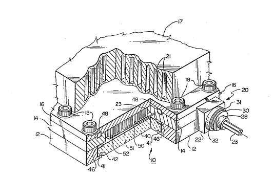
Figure 1 is a cut-away perspective view of a coaxial
cable mounting assembly of this invention interfacing
with a TCM.
Figure 2 is an enlarged cross-sectional view of the
assembled interface between the coaxial cable mounting
assembly and the TCM elements.
Figure 3 is a partial cross-sectional view showing
the passage of the coaxial cable through the coaxial
cable mounting assembly to the coaxial cable connection
site.
FI9-91-053 7 2061~28
Figure 4A is an exploded side view showing the
retainer having a coaxial cable guide groove, and other
related elements.
Figure 4B shows a modified retainer with an inverted
coaxial cable guide groove.
Figure 5 illustrates a seal frame having the
modified retainer of Figure 4B, with alignment means.
Figure 6 is an enlarged view of the coaxial cable
and connection means on a substrate with the partial
guide elements.
Figure 7 is an enlarged view of another embodiment
of the coaxial cable with a coiled delay line and
connection means on a substrate with the partial guide
elements.
Figure 8A is a side view of a modified connector
which is used for connecting the coaxial cable to the MLC
substrate.
Figure 8B is an end view of the modified connector
of Figure 8A.
Figure 9 is an example of a tapped delay line
configuration within an MLC substrate.
DETAILED D~TPTION OF 1~ INVENTION
The novel apparatus and method or the
transmission-line interface of this invention is
comprised of many aspects. The primary aspect of this
invention is the utilization of substrate surface for
electrical communication using a transmission-line, with
little or no effect to other electronic devices that may
be on the substrate. Similarly, the invention also
allows for the modification of the cooling configuration
of a TCM with little or no impact to the cooling
capabilities of the TCM. These and other unique features
of this invention are discussed later in this section.
A transmission-line as used herein means, a coaxial
cable or a twisted pair or a flat stripline, or any kind
of line that will provide at least two electrical paths
where the paths are electrically isolated from each other
and there is a solid dielectric separating the electrical
FI9-91-053 2 0 61~ Z8
paths. Conventionally, these paths are referred to as
the signal path and the ground path.
The transmission-line connection typically has a
signal line as well as a ground line to form an
electrical contact pair. The electrical contact pair
could be on the surface of a substrate or could be formed
in conjunction with an electrical connection means, such
as a connector.
An electronic device as used herein could include
passive circuit elements, such as resistors, capacitors,
and inductors, or semiconductor devices, and associated
circuitry, such as diodes, transistors, and logic
circuits, to name a few.
For the purposes of illustration only in FIG. 1, a
Thermal Conduction Module or TCM 10, comprising a lower
frame 12, an upper frame or hat 16, sandwiching a seal
frame 14, which has been modified, is shown. Other types
of modules could also be used with this invention, such
as the Multichip Module (MCM) or air-cooled module, to
name a few. The lower frame 12, seal frame 14, and upper
frame 16, are held together by securing means, such as
bolts 18. Usually a cold plate 17, having a number of
coolant channels 21, is secured to the upper surface of
the upper frame 16, by means well known in the art. A
substrate 40, having stepped edge 42, and having
semiconductor chips 50, thereon, is secured between the
ledge 41, of the lower frame 12, and the extension of
seal frame 14, with a gasket 46, therebetween. It is
customary to have heat exchange elements 52, such as the
High Conduction Cooling (HCC) elements as disclosed in
European application No. 89480064.8, published November
29, 1989, (Horvath, et al.), to transfer the heat
generated by the chip 50, to the upper frame or hat 16.
For the purposes of illustration only, the upper frame or
hat 16, is discussed in conjunction with heat exchange
element 52, or HCC element 52, but the upper frame could
have any type of a cooling device or structure, for
example, the upper frame 16, could be similar to the one
as disclosed in U. S. Patent No. 4,226,281, or the one
disclosed in U. S. Patent No. 4,235,283. Of course, in
FI9-91-053 9
~- 2~61328
any situation the upper frame 16, would have to be
modified to accommodate a guide or a retainer-like
element, as discussed later in this section. A retainer
51, is normally used to hold the heat exchange elements
52, in place. As discussed later in this section, this
retainer 51, is also used to provide the guide grooves
and securing means for a transmission-line 23, such as a
coaxial cable 23. For the purposes of illustration only
the transmission-line 23, is being referred to as coaxial
cable 23, but, this does not limit other forms of
transmission-lines that can be used with this invention.
In cooling devices or structures where there is no
retainer 51, the cooling device or structure could be
easily modified by a person skilled in the art to provide
means for guiding and securing the coaxial cable 23, from
the exterior of the TCM 10, to a site where the end of
the coaxial cable 23, will be secured on the substrate
40. A fluid tight seal with respect to the interior of
the module that includes the chips 50, that are on the
substrate 40, HCC elements 52, and other related
elements, may be achieved by means of gaskets 46 and 48.
A coaxial cable mounting assembly 20, provides the
interface between the coaxial cables 23, and the TCM 10.
Face plate 22, keeper 32, wave washer 31, retainer 30,
and shoulder 28, are various components of the coaxial
cable mounting assembly 20, that normally protrude out of
the TCM 10.
The coaxial cable mounting assembly 20, may be
located between any adjacent pair of bolts 18, along the
sides of the TCM 10. Therefore, any side of the TCM 10,
may then accommodate (N-l) coaxial cable mounting
assemblies 20, where N = number of bolts along the given
side of the TCM 10. Each coaxial cable mounting assembly
20, has at least one coaxial cable 23. Each coaxial
cable 23, typically has an electrical conductor in the
center, with a low dielectric constant insulator of
suitable thickness over the center conductor, and this
sub-assembly is then encased within a tubular electrical
conductor.
FI9-91-053 10 2 0 613 ~8
FIG. 2 illustrates a view of the elements of the
coaxial cable mounting assembly 20, which provides
penetration through the side of the seal frame 14. The
seal frame 14, has a series of holes 19, to accommodate
the bolts 18. A stress relief sleeve 24, has shoulders
26 and 28, at each end, and also radial grooves 27 and
29, to accommodate retaining rings 47 and 30,
respectively. The coaxial cable mounting assembly 20,
can be prepared by feeding the coaxial cables 23, through
the opening in the stress relief sleeve 24.
FIG. 2 further shows an enlarged cross-sectional
view of the assembled coaxial cable mounting assembly 20,
as part of the seal frame 14, and the upper frame 16, and
lower frame 12. The coaxial cables 23, are passed
through a stress relief sleeve 24, so that a flanged tube
39, is welded peripherally to the bellows 11, at its
shoulder 13. The other end of the bellows 11, is
soldered to the lip 15, on the stress relief sleeve 24,
to effect part of the seal system for the coaxial cable
mounting assembly 20. The flanged tube 39, is extended a
fixed distance from the face of the shoulder 26, and a
spacer is temporarily inserted while the outer conductors
of the coaxial cables 23, are soldered to the openings on
the face of the flange 34. Removing the temporary spacer
allows the coaxial cables 23, to move along the axis of
the stress relief sleeve 24, by compressing the bellows
11, until the flange 34, seats on the face of the
shoulder 26. Conversely, the flange 34, is free to
displace away from the face of the shoulder 26, by
extending bellows 11. The extension of the bellows 11,
is limited by the tab 35, which is part of the bias
spring 101, discussed later in FIG. 5. The constrained
axial displacement of the bellows 11, compensates for the
expansivity differential between the semi-rigid coaxial
cables 23, and the TCM assembly 10.
This sub-assembly can now be fed ihrough the hole in
the seal frame 14, and the face plate 22. The retainer
ring 47, is expanded and then relaxed into the groove 27.
The stress relief sleeve 24, is now pulled away or back
from the seal frame 14, and 0-ring 33, keeper 32, wave
FI9-91-053 11 20S1328
washer 31 and retainer ring 30, are slid in place to
fully secure the stress relief sleeve 24, to the seal
frame 14. This is accomplished by relaxing the retainer
ring 30, into the radial groove 29, which compresses and
securely holds this assembly in place against the face
plate 22. The retainer ring 47, inserted in the radial
groove 27, at the other end of the stress relief sleeve
24, securely locks the stress relief sleeve 24, in place.
The lower frame 12, and the upper frame 16, are
sealed with gaskets 46 and 48, respectively. The gasket
33, provides an effective seal for the coaxial cable
mounting assembly 20. Gaskets 46 and 48, can be an
"0-Ring" or a "C-Ring", type gasket to effect sealing
when assembled to other elements of the TCM 10, using
bolts 18. A pad 43, that is between the ledge 41, and
stepped edge 42, provides a cushion for the substrate 40.
FIG. 3, illustrates a partial cross-sectional view
showing the passage of the coaxial cable 23, through the
coaxial cable mounting assembly 20, to the coaxial cable
connection site 150. This coaxial cable connection site
150, can be placed practically at any location on the
substrate 40. These locations could include the sites
for semiconductor chip 50, or the sites for decoupling
capacitor 74, or between chip edges, to name a few. The
preferred location for the coaxial cable connection site
150, would be to replace a decoupling capacitor 74, and
use that site for the coaxial cable connection. Because,
by removing a few decoupling capacitors 74, there will be
negligible loss in noise immunity, but the removal of a
semiconductor chip 50, could have significant loss in
circuit capacity. Additionally, the replacement of the
decoupling capacitor 74, can be done with minimal design
change of the substrate wiring. The introduction of
these coaxial cables provides a significant increase in
function and low noise communication means.
The thermal expansion differential of the various
materials in the TCM will produce strain on the
semi-rigid coaxial cable 23. This expansivity
differential between the coaxial cable 23, and the TCM
10, can be accommodated by the bellows 11, which has
FI9-91-053 12 2 0 6 ~ 3 28
contraction and expansion capability. The retainer 51,
has openings 66, to accommodate either a coaxial cable
connection, or a decoupling capacitor 74.
It was also discovered that the existing cooling
configuration of part of the upper frame could be
modified to allow containment, passage and alignment for
the coaxial cable. This modification allows for maximum
utilization of the cooling configuration without
impacting the cooling performance. For the purposes of
illustration only, the cooling configuration which is
similar to the cooling configuration of European
Application No. 89480064.8, published November 29, 1989,
(Horvath, et al.) is shown in FIG. 4A, but any existing
cooling configuration can be similarly adapted to be used
with this invention.
In order to position the coaxial cables 23, within
the available space in the TCM 10, a retainer 51, with
guide channel 69, and the upper frame 16, are modified.
These modifications are shown in Figure 4A. The retainer
seat 53, is modified to accommodate the retainer 51. The
retainer 51, must also be modified to provide means for
securely holding coaxial cable connection means, such as
a substrate connector. The upper frame 16, is also
modified by shortening one of the retaining guides or
large fins 56, to form a stub guide 58. The stub guide
58, has a restraining groove 59, or a key depending on
which type of delay is employed. When spirally wound
coaxial cable delay line 71, is used, the tapered slot
55, in FIG. 4A, and the coaxial cable guide 69, are
inverted as shown and discussed in FIG. 4B. The
periphery of the upper frame 16, has a groove to
accommodate gasket 48. The fins 54, on the upper frame
16, mesh with the fins of the HCC element 52, as
described in European Application No. 89480064.8,
published November 29, 1989, (Horvath, et al.). The
retainer 51, is a standard retainer that is used in
conjunction with the upper frame 16, but now has been
modified to have at least one coaxial cable guide 69,
having tapered channel 55, and key 57. The retainer 51,
also has at least one boss 63, with openings 65, to
FI9-91-053 13 2 0 ~1~28
accommodate an eccentric pin 64. A HCC spring 62, is
normally inserted in the openings in the HCC element 52,
and this sub-assembly is then placed in the openings in
the upper frame 16. The retainer 51, and the retainer
spring 60, are then securely attached to the upper frame
16, with the seal frame 14, securely holding this
assembly in place. The retainer spring 60, has openings
(not shown) to allow the passage of the upper surface of
the coaxial cable guide 69, and the key 57, that mates
with the restraining groove 59. The result of this
modification is to provide a coaxial cable guide 69, and
still effect the X, Y and Z-axis movement control for the
heat exchange element or HCC element 52. The coaxial
cable 23, is placed in the tapered retainer channel 55.
The flat spring 60, that is placed between the retainer
51, and the upper frame 16, maintains engagement of the
coaxial cable connector means, such as the substrate
connector, during normal operation and preclude Z-axis
motion and compensates for substrate 40, deflections due
to module connector actuation.
FIG. 4B shows modifications to accommodate spirally
wound integral delay line 71. The transmission-line 23,
is spirally wound so that at least a portion of the
transmission-line 23, can be used to form a spirally
wound delay line 71. Of course the transmission-line 23,
could have one or more of these spirally wound delay
lines 71. The retainer 151, is similar to the retainer
51, as discussed above, except that the tapered slot 55,
is now an inverted tapered slot 155, that is used to
securely accommodate the spirally wound integral delay
line 71, within the coaxial cable guide channel 169. The
delay line 71, is made by spirally winding a portion of
the coaxial cable 23. The restraining groove 59, is
replaced with a matching key (not shown) to accommodate
the inverted tapered groove 155.
In some cases the transmission-line 23, may need to
be electrically isolated from the electronic devices that
are on the substrate, in such cases the retainer 51 or
151, could be electrically isolated from the substrate,
by methods well known in the art, such as coating or
FI9-91-053 14
2061328
anodization, to name a few. This electrical isolation
could also be achieved by coating the naked
transmission-line.
The retainer 151, having sector rib 68, to position
HCC element 52, is assembled through the top of the seal
frame 14, by using two of its adjacent edges to compress
a bias spring 101, located in the inside wall of the seal
frame 14, as illustrated in FIG. 5. Corresponding bosses
121, to bosses 63, on adjacent edges of the retainer 151,
are located on the inner sides of the seal frame 14.
Bias spring 101, is located on the inner sides of the
seal frame 14, to force the retainer 151, against
eccentric pins 64, located on the bosses 121. The
adjacent edges of retainer 151, are made to compress bias
spring 101, so that opening 65, then engage eccentric
pins 64. By rotating either of the eccentric pins 64,
the retainer 151, can be precisely positioned in the X
and Y axis. The substrate 40, can be laterally adjusted
to optimize it for optimum pin/connector alignment and
the eccentric pins 64, rotated to reduce side loading on
the coaxial cables in guide groove 155. When the various
components of the TCM 10, such as lower frame 12, seal
frame 14, upper frame 16, coaxia] cable mounting assembly
20, are assembled, care should be taken that these
components provide a fluid tight seal, as the coaxial
cable connector components and other electronic devices
on substrate 40, must be protected from outside
environmental elements. Also, in some cases, the TCM 10,
may contain a fluidic medium that acts as the cooling or
heat transfer medium for the various electrical
components that are on the substrate 40. The stress
relief sleeve 24, can also be modified to accommodate any
number of coaxial cable connectors. One such connector
is shown as coaxial cable connector 199. Use of such a
coaxial cable connector 199, would make the TCM 10,
modular or be plug-compatible.
FIG. 6 is an enlarged view of the coaxial cable
connection site 150, and it also shows other related
elements on the substrate 40. The substrate 40, can be a
multilayered ceramic substrate 110, as shown in FIG. 9,
FI9-91-053 15
- 20~1328
or any other type of multilayered substrate. The
substrate 40, of FIG. 6, has solder pads 129 and 130, for
soldering the outer conductor 38, and the inner conductor
44, respectively, of the coaxial cable 23. Solder pads
72, are used to connect to solder balls 102, on a
semiconductor chip 50, or to a decoupling capacitor 74
(not shown). The sector rib 68, is used to position the
heat exchange elements 52 (not shown). The retainer 51,
has a key 57, and a coaxial cable guide 69, that contains
the tapered channel 55, as shown and discussed in FIG.
4A. The key 57, in some cases could have openings 104,
to accommodate the flat retainer spring 60, using the
interlock key 49.
The inner and outer conductors 44 and 38, insulated
by an insulated jacket 45, are reflow-bonded on to the
substrate 40 or 110, as, for example, at the vacated
corner capacitor 74, position. Electrical wiring to the
appropriate chips 50, through the vias 181 and 183,
provides the electrical circuit, that is needed to
accommodate the various electrical features of this
invention, such as the master clocking circuitry or
connection to the integral delay line.
The substrate 40, or the multilayered substrate 110,
typically has pins on the underside, which are
electrically connected to metal layers by means of metal
filled vias 181 and 183. This electrical path provides
electrical connection to external circuitry and power
distribution.
FIG. 7, shows a view of a preferred alternative
embodiment of a separable connection means for securing
the coaxial cable 23, to the substrate 40 or 110. The
connector means is preferably positioned along the axis
of the coaxial cable guide 169, and between any pair of
bolts 18, as discussed earlier.
FIG. 7 also illustrates the spirally wound delay
line 71, configured to be integral with the miniature
semi-rigid coaxial cable 23. The delay line 71, re~uires
that the tapered guide channel 155, be relocated to the
top of the guide channel 169. This relocation precludes
electrical contact of the outer conductor 38, of the
FI9-91-053 16 2 0 6 1~ 28
coiled delay line 71, to the pads (not shown) that are
disposed on the surface of the substrate 40 or 110, and
which are located between edges of adjacent semiconductor
chips 50. To accommodate expansion differential between
the coiled delay line 71, the number of coils will be
limited to at least two less than the number of coils
possible within the cylindrical seat 115, located in the
tapered wall channel 155, and the stub fin 58. Located
in the guide member 169, is a connector cavity 129, for
securing the connector assembly 99.
The stub guide 58, which is part of the upper frame
16, is made to engage guide member 169, with keys 128,
interlocked with tapered wall channel 155, to align the
stub guide 58, and the guide member 169. Further, the
triple protrusion 113 and 129, engage the top face of
connector assembly 99, to lock it in place.
The slotted T-shaped contacts 105 and 106, are
bonded to the solder pads 108 and 109, respectively, with
the insulator 107, separating the contacts 105 and 106.
The assembly of upper frame 16, seal frame 14, lower
frame 12, and related gaskets 46 and 48, results in
contacts 203 and 103, as shown and discussed in FIG. 8A,
mating with slotted T-shape contacts 105 and 106,
respectively. The separable connector assembly 99,
provides the electrical path between the coaxial cable
23, and circuit chip 50, through wiring in the substrate
40 or 110.
The connector assembly 99, is shown in front and
side views in FIG. 8A and 8B, respectively. The
connector assembly 99, could be similar to the universal
electrical connector, as disclosed in European
Application No. 89480064.8, published November 29, 1989,
(Harris et al.). The connector assembly 99, has a pair
of back-to-back oriented spring contacts 203 and 103.
The contacts are assembled in individual cavities 130 and
131, so as to be electrically isolated from each another.
Tabs 132 and 133, are curved to pass through matching
curved slots 134 and 135, on the top face of the
connector assembly 99. After insertion of the curved
tabs 132 and 133, through the matching curved slots 134
FI9-91-053 17 2~61328
and 135, tabs 132 and 133, are flattened which captivates
contacts 203 and 103, to the connector assembly 99. Tabs
132 and 133, have slots 136 and 137, respectively, to
accept the center conductor 44, and outer conductor 38,
of the coaxial cable 23. The modified contacts 203 and
103, are normally used for connection to pins (not
shown), located at the bottom of substrate 40 or 110.
Contacts 203 and 103, are double cantilever beams that
engage flat contact element of suitable thickness between
contact locations 138 and 139. The contact cavities 131
and 130, have angled side walls 140 and 141,
respectively, to accommodate movement of the double
cantilever beams 203 and 103. The upper shoulders 143,
the lower shoulders 142, on the connector assembly 99,
are configured to match similar ledges on the connector
cavity 129, as shown in FIG. 7. With the connector
assembly 99, seated in the connector cavity 129, the
outer conductor 38, and the inner conductor 44 are
soldered in slots 136 and 137, respectively, of contacts
203 and 103.
FIG. 9 illustrates an example of a printed wiring
pattern that is embedded in the wiring planes of an MLC
substrate 110. Electrically conductive line 127, is
formed into a serpentine pattern, as shown. The MLC
substrate 110, is configured with equally spaced vias
111. In order to form the tapped delay line the vias
111, are being tapped at various intervals to form via
taps 128. The vias 144, are similar to vias 111, except
that vias 144, can be tapped to form via taps 128. This
sub-division of the original taps allows one to further
fine tune the delay in the electrically conductive lines
127, by these incremental changes. The serpentine
pattern of the electrically conductive line 127, is the
preferred pattern for the tapped delay line, but other
two-dimensional or three-dimensional pattern
configurations across the multilayered substrate in a
multi-planar configuration can be made by a person
skilled in the art. The tapped delay line is used when a
variety of values are desired. Tapped delay lines can be
FI9-91-053 18 2061328
combined with integral coaxial delay elements to tune or
obtain variable delays.
As discussed earlier, the coaxial cable 23, can be
used for communication for clock distribution and
data-bus applications. Typically an electronic clock
distribution system is comprised of a master oscillator
from which a clock pulse train is distributed to
satellite electronic functions, such as a logic chip on a
substrate contained in a TCM. This invention enables the
distribution of clock pulse trains through optimum
transmission lines such as coaxial cables in conventional
TCM. This coaxial cable distribution system relative to
present-day microstrip and tri-plate transmission systems
allows for:
a) reduced skew, i.e., clock pulse arrival time
variation,
b) lower noise at high clock frequencies (greater
than 100 megahertz),
c) increased distance between electrical functions
due to less waveform distortion and coupled-noise,
d) elimination of speed-matching buffers, and,
e) optimization of impedance-matching
terminations.
If an optical clock were to be utilized such as the
one in this invention, a practical implementation would
entail the distribution of a clock pulse train to each
quadrant of the MLC substrate. Further clock
distribution by the electrical nets within each quadrant
then synchronizes the logical operations to a machine
cycle-time for the computer chips.
In the data bus application, high-speed bits of data
must be communicated between memory locations or between
data storage and logic chips. This invention enables the
use of coaxial cables to interconnect chips in tight
bundles of coaxial cables with significantly lower
coupled-noise than current printed circuit wiring.
While the present invention has been particularly
described, in conjunction with a specific preferred
embodiment, it is evident that many alternatives,
modifications and variations will be apparent to those
FI9-91-053 19 2061328
skilled in the art in light of the foregoing description.
It is therefore contemplated that the appended claims
will embrace any such alternatives, modifications and
variations as falling within the true scope and spirit of
the present invention.