Note: Descriptions are shown in the official language in which they were submitted.
-- 1 -- 2
IMPRO~SD ~3AND~TOP ~ILTER
Fiel~ of the_ Il~vention
The invention pertains to band reject, or
"notch", filters. More particularly, the invPntion
pertains to improved band rejezt filters realized using
a plurality of resonators in combination with a stepped
or graded impedance transmission line.
B~okgrou~ o~ th2 I~v~tion
Conventional RF and microwave narrow-band
bandstop filters generally consist of a length of
transmission line or waveguide to which multiple one-port
bandstop resonators are coupled - either by direct
contact, by probe, by loop, or by iris - at spacings of
approximately an odd multiple of a quarter wavelength,
usually either one quarter wavelen~th or three quarter
wavelengths. The individual resonators are typically
quarter-wavelength transmission line resonators, cavity
resonators, or dielectric resonatorsO
It is also known to provide some means o~ tuning
the ~requancy of the resonators, since manufacturing
tolerances and material properties make resonator
~requencies too unpredictable to guarantee optimum filter
performance. Usually, the characteristic impedancP o~ the
transmission line is held constant along its length.
Filters have been implement~A utilizing stripline
technology resulting from a design method which produces
very speci~ic impedance values in a stepped impedance
transmission line. (Schiffman and Youngl "Design Tables
for an Elliptic-Function Bandstop Filter N~5", I~EE
Transactions on Microwave_Theorv and_Techniques~ Vol.
MEET-14 No. 10, October, 1966, pages 474-481). Such
designsl however, tend to suffer from a more complex
configuration, stringent dimensional tolerances,
unsuitability to narrow band applications and excessive
pass band loss.
~r~ V~.
2 ~
With prior art narrow-band b~ndstop filters,
the unloaded Q of all ~f the resonators must
be maximized to achieve the best performance, while their
level of coupling to the transmission line mu~t be
individually adjusted to obtain the best performance.
UnfortunatPly, given a transmission line of con~tant
impedance, the optimum values of thes~ couplings may
exceed the maximum achievabl~, or desirable, with a
given coupling method. For a fixed number of
resonator~, the per~ormanc~ o~ ~he filter ~hen becomes
limited b~ the maximu~ achievable coupling rather than
by maximum obtainable unload Q of the resonators.
Under such circumstances, the optimum ~ilter
performance cannot be realized.
While equal-ripple stop band, constant-
impedance transmissîon line notch filters are known,
and given a maximum achievable or desirable level of
coupling o~ the resonators to the transmission line, it ~:
would be desirable to achieve:
similar or better performance
(notch depth, selectivity, and
bandwidth) with fewer resonators,
greater notch selectivity
(ratio of notch floor width to
width between passband edges~ with
similar or better notch depth,
and greater notch depth
(greater level of band re~ection)
with similar or better notch
selec~ivity.
In addition, ~rom a manufacturing and -
installation point of view, it would be desirable to
achieve reduced sensitivity of each resonator~s
characteristic resonant fre~uency to the coupling
mechani~m which couples between the resonator and the
transmission line. This would provide improved
. . ~
`' . : ' '. , :
mechanical and temperature stability ~or the filters,
better repeatahility of electrical performance from
device to device, and less interaction between the
tuning of the coupling and the tuning of the resonant
frequency o~ a resonator.
Fur~her, it would be desirable to be able to
create a variety o~ no~ch ~ilters using a plurality o~
relatively s~andar~ elements such as resonators
transmission line segments and coupling elements
without having to create a large variety of specialized
components which are only usable with a given filter
design.
8ummary of tha Invention
Notch filters in accordance with the present
invention utilize a plurality of substantially
identical resonators and a stepped or graded imp~dance
transmission line. The transmission line has an input
end and output end. Further, a first selected, centrally
located section of the line has a relatively
high impedance value with at least some of the members
of the plurality o~ resonators coupled to the line and
selectively spaced from one anotherO
Selec~ive spacing of the resonators is on the
order of an odd number o~ quarter wavelengths of the
nominal center ~requency o~ the filter~ Thus, the
resonators can be spaced one quarter wavelength from
one another or three quarter wavelengths from one
another.
Such filters also include first and second
quarter wavelength impedance transforminy sections with
a first trans~ormer section coupled to the input end of
the transmission line and with the second transformer
section coupled to the output end thereof. Each o~ the
transformer sections has an impedance value which is
less than the impedance value of the transmission line.
~ ?~
An input signal can be applied to the first
impedance transformer ~ction and a load can be coupled
to the second impeda~ce transfoxmer section. The
described notch filters provlde high performance with
a deep, though relatively narrow, attenuation region.
The resonators are tuned to di~ferent
frequ~ncies in either consecutively increasing or
decreasing frequenci~s along the filter. The
incremental increase and decrease in tuned ~re~uencies
from the nominal center frequency of the filter can be
the same for a given pair of resvnators.
A notch filter can be implemented with two or
more resonant cavities~ some of which will be spaced
along the relatively high impedance~ central,
transmission line section. Others of the resonators
may be spaced along the quarter wave impedance
transformer sections, each o~ which has an impedance
less than that of the transmission line. Still others
may be spaced alsng input and output transmission line
segments ha~in~ yet lower impedance ~alues.
The filters can be implemented with either a
relatively straight transmission line segment or a
folded transmission line segment which results in a
smaller physical package. Resonators are spaced from
one another along the relatively high impedance
transmission line on the ~rder of an odd number of quarter
wavelengths.
The resonator units can be implem~nted with
cylindrical conductive housings containing dielectric
resonator members. The resonator units can be
implemented with adjustable resonant frequencies for
purposes of setting up and tuning the filter. The
re~onators ~ach include an adjustable coupliny loop.
Increasing the value of the characteristic impedance o~
the txansmission line through the interior region of
.... . . .
.- , . . .
, ' :', ' . : ~ ' ~
,
- 5 ~
the ~ilter e~fectively increases the coupling to the
respective resonators.
In yet another embodiment, the lengths of
members of pairs of selected sections of the
transmission line, linking adjacent resonator~, can be
respectively increased and decrease~ by predetermined
amounts. Such modifications result in filters
requiring fewer resonator cavities for achieving
substantially the same level of performance as is
achievable with quarter waveleng~h tra~smission line
sections.
Additionally, selected transmission line
sections, linking adjacent resonatorsr can be reduced
in length a fixed amount for a given filter. Thi~
reduction takes into account or compensates for the
effects the coupling elements have on effec~ive line
length. By way of example, the compensating reduction
in length of quarter wavel~ngth sactions can be in a
range of eleven to twelve degrees of the center
frequency of the filter.
Numerous other advantages and features of the
present invention will become readily apparent from the
following deta;led description of the invention and the
embodiments thereof, from the claims and from the
accompanying drawings in which the details of the
invention are fully and completely disclos~d as a part
of this specification.
Brlef De~oriptio~ of the Dra~i~
Figure 1 is an overall block diagram of a
filter ha~ing ~ix resonators;
Figure 2 is a perspective mechanical view of the
filter of Figure I;
Figure 3A is a graph illustrating relatively
broadband ~requency characteristics of the filter of
Figure I;
-- 6 --
Figure 3B i5 a secc~nd graph illustrating
relativsly narrow band characteri~:tlcs ~f the filter of
Figure l;
Fiyure 4 is a perspective view of an
alternate embodiment of the filter o~ Figure I;
Figure 5A is a graph illustrating relatively
broadband ~r~quency characteristics of the filter of
Figure 4;
Figure 5B is a second graph illustrating
lo relatively narrow ~and characteristics of the filter of
Figure 4;
Figure ~ is an overall block diagram of a
filter having two r~sonators;
Figure 7 is a perspective view, partly broken
away, of the stepped impedance line of the filter o~
Figure 6:
Figure 8 is an enlarged partial view, partly
in section, illustrating details of the resonator
coupling loop;
Figure 9 is a graph illustrating the
frequency characteristics of the filter of Figure 6;
Figure 10 is a schematic diagram of a filter in
accordance with the present invention;
Figure 11 is a graph illu~trating the :
~requency characteristics of the filter of Figure 10;
Figure 12 is a graph illustrating the
freq~ency characteristics of a compensated version of the
*ilter of Figure 10; and
Figure 13 is a schema~ic diagram, exclusive
of resonators, o~ yet another embodiment of a filter in
accordance with the pre~ent invention.
Figure 14 is a generalized ~chematic block
diagram view of a filter in accordance with the present
invention having an odd number of resonators;
Figure 15 i~ a generalized schematic block
diagram of a ~ilt~r in accordance o~ the present invention
.
.
,,'7~J~
~ 7 --
having an even number of resonators;
Figure 16 is a block diagram schematic of a 3
resonator filter in accorda~ce with the present inve~tion;
Fiqure 17 is a block diagram schematic of a 4
5 resonator filter in accordance with the present invention;
Figure 18 is a block diagram schematic o~
another 3 resonator filt~r in accordance with the present
invention: and
Figure 19 i8 a block diagram schemat~c oE
lo another 4 resonator ~ilt~r in accordance with ~he present
invention.
Det~ile~ De~crlntion of the Preferred Embodiment~
While this invention is susceptible of
embodiment in many di~ferent forms, there is shown in
the drawing and will be d~cribed herein in detail
specific embodiments thereof with the understanding
that the present disclosure is to be considered as an
exempli~ication of the principles of the invention and
is not intended to limit the invention to the specific
embodiment illustrated.
The present invention relates to a family of
notch filters which have common structural
characteristics. A stepped impedance, common
transmission line provides a signal path betwe~n input
and output ports of the filter.
A plurality of resonators is used fox
creation, in part, o~ the desir~d ~ilter
characteristics. At least some o the resonators are
electrically coupled to a relatively high impedance
s~ction of the tran~mission line. Other resonators can
be coupled to lower impedance sections of the
transmission line.
Coupled to each end of the relatively high
impedance transmission line is a quarter wavelength
impedance trans~ormer. The impedance transformer
sections hav~ a lower impedance than the central
~.
... . .
- 8 -
section o~ ~he ~ransmission line. It will be
understood that other types o~ impedanc0 transformers
can also be used.
Input and output signals can be applied to
and derived directly from the impedance transformer
sections. Alternately, a lower impedance transmission
line seation, with the same impedance as the source or
the load can be coupled to each of the quarter wave
impedance transformer~.
Additional resonators can be coupled to the
input and output transmission line sections to further
improve and/or refine the fllter per~ormance
characteristics.
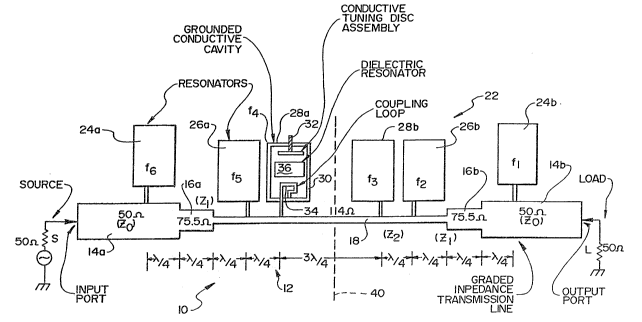
With respect to Figure 1, a notch filter 10
~5 is illustrated. The ~ilter 10l illustrated in block
diagram ~orm, can be coupled to a source S having, for
example, a 50 ohm characteristic impedance and a load
h having, for example, a 50 ohm impedance.
The filter 10 includes a stepped impedance,
multi-element transmission line generally indicated at
12. The transmission line 12 include6 50 ohm input and
output transmission line section~ 14a and 14b.
Each of tha 50 ohm ~ections 14a and 14b is in
turn coupled to a quarter wav~ impedance transformer
sectîon 16a and 16b. Each quarter wave imp~dance
transformer 16a and l~b has a characteristic impedance
value which exceeds th~ impedance value of the input
and output transmission lin sections 14a and 14b.
A central, higher impedance transmission line
section 18 is coupled between each of the impedance
transformers l~a and 16b. The transmission line
section ~8 has, in the present in~tance, a
characteristic .impedance on the order o~ 114 ohms. The
quarter wave trans~ormer ~ctions 16a and 16b each hav~
~5 a nominal i~pedance value on the order o~ 75.5 ohms
(actual realized value was 71.2 ohms). The input and
,
.. .. . .
.~. .
output transmission line sections 14a and 14b each have
a ~tandard nominal charac~eristic impedance of 50 ohms
tactual realized value was ~9 . 8 ohms) .
A plurality of substantially identical
resonators 22 is coupled to various elements of the
multi-impedance transmi~sion line 12. For example,
r~sonators 24a and 24b are each coupled to a respective
input or output transmission lin~ segment 14a or ~4b.
~he resonators 24a and 24b are spaced one-quarter
wavelength from the adjacent respective impedance
transformer 16a or 16b.
Resonators 26a and 26b are coupled to the
high impedance segment 18~ Each of the resonators 26a
and 26b is located one quarter wavelength away from thP
respective impedance transformer 16a or 16b.
Re~onators 28a and 28b are also each coupled
to the high impedance transmi~sion line e~ment 18.
The reRonators 28a and 28b are each loca~-ed one quarter
wavelength away from the respective resonators 26a and
~0 26b and are spaced from each other an odd number o~
quarter wavelengths.
Each of the re~onators 24-28 consi~ts of a
high Q dielectric resonator 36 supported with Iow loss
dielectric within a co~ductive cylindrical housing 30,
illustrated with respect to resonator 28. Eash of the
resonators includes an ad~ustable, conductive,
frequency tuni~g disk a~sembly 32.
Further, each of the resonators includes ~n
ad~ustabl~ coupling loop 34 ~or coupling to the
ad~acent transmission line segment. It will be
understood that alternate coupling members such as
probes or irise5 could be used without departing from
the spirit and scope of the present invention.
The coupling loop 34 can be rotated during
set up and tuning to obtain ~he amount of coupling
which optimizes filter perfo~mance. The coupling loop
-, , ~ ~ . . . .
'' '' ~ ~
.
-- 10 --
34 ha~ an axis which is preferably lined up with an
edge of the resonator 36.
The transmission line 12 includes an outer,
hollow conductor which could, fox example, have a sguare
or rectangular inner cross section and a wire
inner conductor. The inner conductor is supported
along its length. Support ~an be provid~d either by a
dielectric materi~l, such as TEFLON or REXOLITE, whioh
is used to set the impedance value of a section or by
relatively thin dielectric supports when the desired
impedance and geometry of tha line re~uire air as the
dielectrlc material.
The characteristic impedance value of each of
the various sections such as 14a, 14b, 16a, 16b and lS
is established by adjusting the dimensions of the inner
and outer conductors as well as the dielectric constant
and dimensions of the supportin~ material in each of
those sections. The values o~ each of the re~p~ctive
impedance~ are approximately related in accordance with0 the following well known eguation:
zl2 = Z0 * Z2
~ he filter 10, it should be noted is
symmetric about a center line 40. The resonators are
tunad in ascending or descending order to achieve the
desired overall ~ilter performance.
It will be understood that while the above
values are preferred that physical realizations of the
~ilter 10 may result in variations from the indicated
values. One advantage o~ the structure o~ ~ilter 10 is
that over-all filter performance is not significantly
impactQd by such variations since resonatoræ 24~28 have
ad~u~table coupling to the transmi~sion lin~ and
adjustable resonant ~requencies.
The xe~onators are tuned in ascending or
descending ~requency order to achieve the desired
overall ~ilter performance. In ~ilter 10, resonator
24a is tuned to the highest stopband ~requQncy f6 while
resonator 26a is tuned to the next lower fr2quency ~S,
and so on, with resonator 24b tuned to the lowest stop
band frequency~ fl. JU5t as the r2sonators are
symmetrioally placed about th~ physical centerline o~
the filtar, the frequencies that the respective
cavities are tuned to t~nd to be approximately
symmetric about the renter frequ~ncy o~ the filter, as
is evident in the graphs of the measured ~ilter
frequency response.
Table I lists an exemplary set o~
frequencies, f1 through f6, for a filter as in Figure 1
with a center stop band frequency ~0. In Table 1 all
~requencies or variations thereof are in MHz.
TABLE 1
f1 = 845 240 - ~ - O 510
f2 = 845.360 = fo _ 0.390
f3 = 845.585 = ~0 - 0.1~5 fO
845.75~ .
2~ f4 = ~45.875 = ~0 ~ ~.125
f5 = ~4~.140 = ~0 + 0.390
f~ = 84~.260 = fO ~ 0.5
FREQUENCY PLAN FOR 6
RESONATOR FILTER
Fi~ure 2 is a perspec~ive view of the filter
10 illustrating relative placement o~ the resonators
24-28 along the stepped impedance transmission lin~ 12.
As illustrated in Figure 2, tha filter 10 utilizes an
essenti~lly straight transmissîon line 12.
Each of the resonators in the filter 10 has a
diameter on the order of ~.5 inohes. The total
overall filter length from input port to output port is
on the order 38.5 inohes.
The ~ilter 10 has been designed to hav~ a -
20 dB stopband bandwidth of 1.0 MH2 centered between
passband -0.8 d~ band ~dges at 845 MHz and 846.5 MHz.
.;
,
:
- ~
:
`J J~ ,3L,
-- 12 --
In addition, it has been designed to have an insertion
loss of l~ss than 0.3 db at 835 M~z and 849 MHz.
Figure 3~ is a graph 50 illustrating the
measured gain (S21) o~ a physical realization of the
5 ~ilter lO as in Figure 2 sver a 14 NHz bandwidth from
835 MHz to 849 MHz~ Each horizontal division of the
graph 50 of Figure 3 ¢orresponds to 1.4 M~z while each
vertical division corre~ponds to .ldB.
As illustrated by the gxaph 50, the ~ilter 10
exhibits a highly selective notch in its frequency
characteristic in the 845 to 846.5 MH~ range.
A se~ond graph 52 on Figure 3 illustrates the
input return l¢ss (S11) of the filter 10 over the same
fre~uency range. Each vertical division for the graph
52 corresponds to 4dB.
Figure 3B illustrates in detail the notch
characteristic of the filter 10. A graph 50a i5 the
gain of the filter 10 over an 844.25 to 847~25 MHz
bandwid~h. Each vertical ~ivision of Figura 3B
corresponds to 4dB. Graph 52a i5 the input return los~
for the filter 10 over the same frequency range. In graph
50a each of the minimums, such as 50b, 50c,
corresponds to a frequency to which a respective
resonator 26b, 28b has been tuned.
Again with respect to the ~ilter lO of Figure
2, the overall cross sectional shape of the
transmission line 12 is square with ext~rior dimensions
on the order of l"xl".
Figure 4 illustrates an alternate six
resonator confiyuration 60. The filter 60 has a block
diagxam which corresponds to the block di~gram o~
Figure 1 and has the same number of resonators. Each
resonator has the ~ame basic configuration as in the
filtex 10.
The filt~r 60 is folded and is physically
smaller lengthwise than the ~ilter 10. The fllter 60
.
- 13 -
includes a folded multi-stepped kransmission line 12a,
having stepped impedances corresponding to the
impedances o~ the transmission line 12. However, the
transmission line 12a has a r~ctangular cross-~ection
with the beiyht of 3~8 of an inch and a width o~ one
inch. It can be formed by milling o~ a c:hannel in an
aluminum block.
Figure 5A ls a plot corresponding to that of
Figure 3A illustrating the filter gain ~S21) versus
~requency response 62 of the filter 60 as well as the
input return loss 64 over the ~ame frequency range 835
MHz to 849 MHz as in Figure 3~. The vertical scale ~or
the return loss 64 is 0.1 dB/division, while the
vertical scale for the insertion loss 62 is 3
~B/division.
Figure 5B illustrates the notch
characteristic o~ filter 50 with horizontal divisions
as in Figure 3B. The insertion loss ver~ical scale is
5 dB/division and the re~urn loss vertical cale is 3
dB/division.
The folded filter 60 is on th~ order of 18.25
inches long and ll.o inches wide.
Fi~ure 6 is a block diagram of a two
resonator filter 70. The filter 70 includes a stepped
impedance transmission line 72 with a relatively high
impedance central section 74 which i5 connected at each
end thereo~ to quarter wave impedance txansformers 76a and
76b. The filter 70 can be fed at an input port 7&a ~rom
a source S of characteristic impedance Zos (far
example 50 ohms) and will drive a load L of impedance
ZOL ( ~Or example 50 ohms) from an output port 78bo
The filter 70 also includes first and second
resonators 80a and 80b which are of the same type D~
resonators previously discussed with respect to the
~ilter 10. The resonators 8Qa and ~Ob are coupled to
the high impedance transmissisn line section 74 and are
' ~,. :
spaced ~rom one another b~ approximately one quarter
wavelength of the center frequency of khe filter 7~.
The filter 70 provides a -18dB deep, 200 KHz
wide notch in a ~requency band 849.8 to 850.0 ~z with
less than 0.3 dB insertion 105S at 849 MHz- The ~.ilter
70 (as well as the filter 10) can be provided with
enhanced performance by ~hortening the quarter
wavelength section between resonators 80a and 80b about
13% or an amount in the range of eleven to twelve
1~ degrees of the nominal center ~requency o~ the notch of
the filter.
.Figure 7 is a perspective view partly broken
away of the transmission line 72 of the filter 70. The
transmission line ~2 has a generally square cross-
section with an ou~er metal housing ~2 with dimensions
on the order of ll'xII'. The housing 82 could be formed
for example of aluminum.
An interior conductor 84 extends within the
exterior metal housing 82 and has a circular cross
section. The conductor 84 can be formed of copper-clad
steel wire for ~xample.~ Such wire has a lower
coeffi~ient of thermal expansion than does copper.
~he interior conductor 84 is supported by
dielectria members 86a and 86b, each of which also has
a ~quare cross-section. The metal housing 74 includes
first and sacond ports 88a and 88b which receive an
elongated couplin~ member from a resonator coupling
loop, ~uch as the coupling loop 34.
The overall length of the transmission line
72 is on the order of 11-I/2 inches with the high
impedance region 74 having a length on the order of 7
inches and an impedance Z2 on the order o~ 114 ohms.
~he two quarter wavelength impedance transfo~ming
sections 76a and 76~ each have a length on the order of
2O2 inches.
.. .
, ~- ' ' ' ' ; ", .
,
. . :
.
- 15 -
The impedance transfoxming sectlons 76a and
76~ each include a dielectric material available under
the trademark REXOLITE. The impedance Z1 of realized
versions o~ the sec~ion 76a and 76b is on the order of
71 ohms as oppo~ed to the design value of 75.4 ohms.
Figure 8 illustra~æ one o~ the adjustable
coupling loops 34 which has an elongated cylindric~l
coupling member (a conductive metal post) 90 which is
ln electrical contact with the central conductor 84.
lo As illustrated in Figure 3, the coupling loop 34 is
adjustable via a manually moveable handle 92 for
purposes of adjusting the coupling to the respective
resonator.
The post so of the loop 34 is insulated from
the collar 94a by a REXOLITE sleeve. Adjustment of the
coupling loop take~ place by rotating metal collar 94a,
attached to handle 92, which is in turn soldered to a
portion 94b of the coupling loop 34. The collar 94a is
in electrical contact with the outer metal conduckor 82
and with the xesonators metal housing 30. ~ teflon
support 96 is provided beneath the rotatable member 90,
for supporting the inner conductor 84 below the
coupling post 90.
Figure 9 includes a graph 96a of the gain of
the ~ilter, 70 and a graph 96~ o~ the input return loss
of the filter. Figure 9 has a 2MHz horizontal extent
with ea~h division corresponding to 3dB.
Figure 10 illustrates in a schematic view an
alternate embodiment lOo of a five resonator filter
which has characteristics and performance similar to
those o~ the six resonator filter 22 illustrated in
Fi~ure 1. The filter 100 o~ Figure 10 includas a
variable impedance transmission line ~02 having an
input and 102a and an output end 102b.
The transmis~ion line 102 can be formed with
a struc~ure similar to the structure of the
, : ~
;
,:
. - 16 ~
transmission line 72 of Figure 7. The transmission
line 102 includes first and second input sections 104a and
104b, each of which includes a TEFLON dielectric
member and each o~ which has a characteristic impedance
on the order of 50 ohms.
Section 104a can be o~ any length. Section
104b is a quarter wavelength section.
Adjacent to the input section 104b is an
impedance transPorming section 104c which includes
REXOLIT~ dielectric material. ~he impedance
transforming s~ction 104c is a guarter wavelength
~ection ~hat has a characteristic impedance on the
order of 73 ohmsO
The central region of the transmission line
102, indicated generally at ~04d, is formed of a
plurality o~ quarter wavelength ~ections containing air
as a dielectric materialO Each of these sections has
a characteristic impedance on the ordar of 114 ohms.
Between the central region 104d and the
output end 102b, the transmission line 102 includes a
further quarter wav~length section 104e with a REXOLITE
dielectric materi~l therein, Comparable to section
104c, as well as two output sections 104f and 104g,
each of which has a characteristic impedance on the
ordex of 50 ohms.
Th~ output section 104g can be of an
arbitrary length. The section 104f is a quarter
wavelength section.
Cavity resonatorsl such as the resonators 24,
26 and 28 of Figure 1, are coupled to the transmission
line 102 at a plurality of ports 106a~106e as indicated
in Figure 10. Unlike the ~ilter 10 of Figure 1, the
filter 100 has only three resonators in the central
section 104d. Further, unlike the ~ilt2r 10 o~ Figure
1, wherein the resonators 26a, 26b, 28a and 28b are
spaced along the central portion of the transmission
L
-- 17 --
line with an odd number o~ quarter wavelengths between
each, the length~ of sections 108a and 108b have each
been modified as have the lengths of the seckions 108c
and 108d. The sections 108a-108d are located on aach side
of a center line 110 for the transmission line 102.
The filter 100 o~ Figure 10 will exhibit
assentially the same type o~ performance with five
r~sonators as does ~h~ ~ilter 10 of Figure ~ usiny six
resonators.
The implementation o~ the filter 100 is
accomplished by adjusting the length vf transmission
lines section 108a in combination with 108b and by
adjusting the length of section 108c in combination
with adjusting the length o~ section 108d.
The spaciny of the section 108a is increased an
amount X12 corresponding to an amount X12 that the
section 108b is decreased. Similarly, the length o~
the sec~ion 108c is increased an amount X23
corresponding to an amount X23 that the section 108d is
decreased in length.
The actual am~unts X12, X23 of in~rease or
decrease of the lengths of the sections 108a-108d can
be datermined by using a method o~ elliptic ~unction
filter design published in an article by J. D. Rhode~
entitled "Waveguide Bandstop Elliptic Function ~ilters"
in November o~ 1972 in the IEEE Transactions on Microwave
Theory and_Techniques. That article is
hereby incorporated herein hy re~erenceO
Altarnately, the i~cremental increases and
decreaseæ X12, X23 to the lengths of the sections 108a-
~08d may be arrived at by iterative optimization using
a commercially availabl~ circuit simulation computer
program. One such simulation program is markated by
EEso~ entitled "TGuchstone".
Using the above noted method derived in the
~hodesl article, the variation X12 o~ the length of
. . . -:
- 18 -
sections 108a and 108b from a quarter wavelength
section is on the order of 23.62 degrePs. In a
raalized filter with a stop band centered at 845.75
MHz, the length of a quarter wavelength ~ection from
the center region 108d is on the order of 3.49 inches.
Hence, the length o~ the section 108a as increa~ed is
on ~he order of 4.4 inches. The decreased length of the
cection 108b, decreased t~e same amount X12 as section
108a has been increased, is on the order of 2.57
inches.
The incremental variations X23 ~ the length
of each of the sections 108c and 108d from a quarter
wavelength are on the order of ~1.6 degreesO Hence,
the length of section 108c has been increased to a
length on the order of 3.94 inches and the section 108d
has been decreased similarly to a length on the order
of 3.04 inches.
Figure 11 illu~trates a graph of a realized
embodiment of the ~ilter 100 illustrating in a curve
112a the insertion loss and in a curve 112b khe return
loss for the filter. Thus, as illustrated by a
comparison of the diagram of ~igure 3b to the diagram
of Figure 1~, results comparable tG that achievable
with a ~ix resonator ~ilter, having quarter waYelength
spacing~ between filters in the central section 18 of
the transmission line can be achieved by using a ~ive
resonator ~ilter, as illu~trated in Figure 10, with
some of the quarter wavelength center sec~ions of the
transmission line altered as described previou~ly.
The performance o~ the filter 100 (as well as
the filters 10 and 70 as noted previously) can be
~urther improved by compensating for ef~ects o~ the
coupling loop assemblies, such as assembly 34 as well
as other stray reactance ef~ects which might be due to
each resp2ctive resonator by reducing the electrical
length o~ ~ections 108a-108d, a uniform amount on the
.
.
-- 19 --
order of 11-12 degrees, by way of example, of the
center ~requency of ~he notch of the ~ilter. For
example, t~e ~lectrical length of the noted ~ections
can be reduced an amount on ~he order o~ 11.3 degrees.
Sec~ion 108a now has a length on the order o~
3.97 inches, sectlon 10~ has a leng~h on the order of
2.14 inches; section 108c has a length on the order of
3.50 inches and section 108d now ha~ a length on the
order of 2.60 inches. ~5 illustrated in Figure 12, as
a result of such a common reduction, the performance of
the filter loO becomQs more symmetric with respect to
the center frequency.
The plots of Figure 12 illustrate that the
overall performance o~ the ~ilter loo ~a~ been improved
~om a point o~ view of the ~ymmetry with respect to
the center freguency of the filter. In addition,
Figure 12 alqo illustra~e~ that minor variation~ in
the length o~ quarter w~velength sections in the
central .region 104d, such as might be e~countered in a
normal manufacturing environment, indicate ~hat overall
filter performance is not extr~mely sensitive to cavity
spacing. Hence, filter designs of the type illustrated
in Figur2 10 tend to be readily manufa~turable to
nominal speci~ications in a normal manufacturing
environment.
Table 2 illu~trates an exemplary frequency
plan ~or the five re~onator filter of Figure 10.
Frequencieæ or incremental variations thereof are
exprassed in MHz.
~Q ~ L2
= 845.225 = ~0 - 0.525
f2 = ~45.375 ~ ~0 - 0.375
~3 = 845.750 = fO fo
845.750
f4 - 8~6.125 ~ ~0 ~ 0.375
f5 = 846.275 = fO + 0.5~5
.
~' :
?~
-- ~o --
TRE~ NCY PI.A~ FOR 5
RE~ONA9:0R IIPIL~B~
In the scheme o~ Table 2, two outside resonators
are tun~d to fre~uenci~s ~1~ f5 an equal
amount, .525 ~Hz,from th~ center band stop freguency fO
of 845.750 MHz. Similarly, two corresponding int~rior
resonators are each tuned to frequencies f2, f4 that
vary ~rom the center frequency fO on the order of .375
~z .
It will be under6tood that either an odd
number or an even number of resonators can be used
without departing from th~ spirit and scope of the
present invention.
Figure 13 illustrates a six resonator filter
120 which incorporates a stepped impedance ~ransmission
line lO3, of the type illustrated in Figures l and lO.
The filter 120 includes quarter wavelength ~ections
122a and 122b each of which is located adjacent to a
respective coupling port lO6b, 106d at which a
respective tuned resonator can be coupled to the
transmissio~ line 103. Further, the ~ections l~2a and
122b have be~n increased and decreased a respective
amount Xl2, as discus~ed previously, ~rom a quarter
wavelength section~
The filter l20 also includes modi~ied
sections 124a and 124b each of which has been altered
in length from a quarter wavelength section hy an
amount X23 as discussed previously. The altered
sections 124a and 124b are associated respectively with
port~ 106d and 106f through which tuned re~onators
would be coupled to the transmis~ion lin~ 103.
It will also be understood that the
impedance~ of the various transmiss.ion line sections
illustrated in Figures lO and 13 correspond generally
~5 to ~hQ impedance value~ indicated in ~igure 1
t~ansmisslon line ~ctions with corresponding types of
:
- 21 -
dielectric materials. The filter 120 can further be
compensated by shortening each of the sections 122a,
122b, 124a, and 124b a common amount k on the order of
11 to 12 degrees of the center stop band ~requency o~
the filter. This compensation as discussed previously
compensates for reactance coupling effects of the
respective resonators.
Figuras 14 and 15 in combination with Table
3 below disclose more ~eneralized representations of
the previously discussed filters which embody the
present invention. The filter of Figure 14 has an odd
number of resonators, comparable to the structure of
Figure lO. The ~ilter of Figura 15 has an even number
of resonators, comparable to the structure of Figure
13.
Table 3 illustrates various relationships, in
accordance with the present invention, for the filters
o~ Figures 14 and 15. In ~he left-most column o~ Table
3 each of those filters includes one or more impedance
sections shortened by an amount k to compensate for the
effects of transmis ion lin~ discontinuities, impedance
transitions and/or non-ideal coupling mechanisms. K
can be used to improve the s~mmetry of th2 return loss
and the inæertion loss characteristic~ of the filter or
can be u~ed to purposely skew them to achieve a desired
charactexistic. Further, in the middle column oP Table
3 modi~ications to various impedance line ,sections are
illustrated which xesult in improved filter performance
as previously discussed.
The right-most column o~ Table 3 indicates
relationships ~or various transmission line seqmen~s
associated with the impedance trans~ormer section such
as sections 16a and 16b o~ Figure l~ Use of these
sections increases the ef~ective coupling of the
resonators to the higher impedance central transmission
line section and resul~s in enhanced per~ormance as
. .
- : ., . , , ~:
. .
;
- 22 ~
described previou~ly. The input and output sections
identi~ied as E and E' in ~igure~ ~4 and 15 can be of
any desir~d length. The values of k, X12 and X23 can be
~ero or greater as di~cussed previously.
q~ABLB 3
I~peda2~G~ ~ra~3former
Co3npansa~e~1 Modig~ie~l 8ect~o~ Enh~nc:e~!l
A--.n1*900-k
B=n2*90-k B'=B-~X23
10 B~=n3*gO-k B =BI-X23
C=n4*900-k C~=C~X12
C'=nS*90-k C~=C'-Xl2
C~ , for
n4=l
D = m4*90, for n4>3
C~ , for n5~1
D' = m5*9O, for n525
nj is an odd integer greater than or e~ual to
one for i=l to 5 in the table above.
mj is an odd integer greatex than or e~ual to
one and less than nj for i = 4 and 5 in the table above.
It will be understood that impedance
transformers, other than transmission line sections,
can be used without departing from the spirit and ~cope
of the present invention. Figures 16-19 illustrate
~chema~iaally alternate filter structures in accordance
with the present invention. In Figures 16 and 18 an
odd number of resonators is disclosed. In Figures ~7
and 19 an even number of resonators is disclosed~
In the ~ilter oP Figure 16, an odd number of
resonator~ 150a - 150c, i5 coupled via coupling means,
such a~ coupler 152 to a ~ixed impedance transmission
line 154. The lin~ 154 terminates in first and second
impedance transformers 156a, 156b.
As illustrated in Figure 16, line 154 is
divided into a region 154a having a length "A" and a
.:
. -
.. ~ ., .
.
2 ~ ~J,,J_ /~ "~
region 154~ having a leng~h "~". A cent~r li1ne 15~c i5
il~ustrated about which ~here is pairwi~ symmetry in
resonator frequenci~s.
The resonator fre~uencies bear the follnwing
relationships to one anoth~r.
f3 > f2 >
fo = f2 = f1~
The lengths A and B can be determined as
1~ follows:
A - nl *90 + x--k
B = n2 *90 ~ x-k
nl and nz are odd integers that are greater
than or equal to one. The value o~ k can be any amount.
One of x or k can also equal zero.
In the Filter of Figure 17/ an even number of
resonator~, 150a - 15Qd, is coupled to the ~ixed
impedance transmission line 154. Corresponding elemen~s
in Figure 17 carry the same identification numerals as
in Figure 16.
Figure 17 illustrate~ a center region 154d
about which there is pair wise symmetry in resonator
frequancies. The values of A, B, x and k are determined
as above. The length of the region 154 can be
determined from:
C = n3 *9o - k
n3 is an odd integer greater than or equal to
~ne. The resonator frequencies bear the following
relationships to one another:
~. , .
-: ~
' ' .
.
f4 > ~3 >
f = f2 + f3 = ~
~ 2 2
ln the filter of Figure 1~, an odd number of
resonat~rs 150a - 150c is coupled, in part, ~o a
centrally located, fixed impedance transmission line
160, and in part to spaced-apart fixed .impedance
transmission lines 162, 164.
The line 160 has an impedance Z2 ~he lines
162, 164 each have an impedance Z~ where Z2 ~ Zo
The values of A, B in Figure 18 are determined
as are the corresponding values in Figure 16. The
fre~uencies of the resonators of Figure 18 bear the same
relationship to one another as do the frequ~ncies of the
resonators of Figure 16.
In the ~ilter o~ Figure 13, an even number o~
resonators, 150a - lSOd, is coupled to constant
impedance transmission lines 160, 162, and 1~4.
Elements in Figure 1~ which corre~pond to elements in
Figures 16 -18 have been assigned the same
identification numeral.
The values of AtB, C of Figure 19 can be
determined as described above in connection with Figure
17. The frequency relationships for the filter of
Figure 19 are the same for the filter of Figure 17. In
Figure~ 10, 13, 16 - 19, lengths of fixed impedance
,
- 25 -
transmission lines indicat2d by the symbol "L'l can be
any con~enient length.
From the foregoing, it will be observed that
numarous var.iations and modifications may be e~fected
without departing from the spirit and cope sf the
novel concept of the invention. It is to be understood
that no limitatîon with respect to the spe~ific
apparatus illustrated herein is intended or should be
~n~err~d. It is, of coursel intended to cover by the
appended claims all such modi~ications a~ fall within
the scope of the claims.
.
'
',, , ,- "' ' ' ' ' . ~ '' " '"' ' ' . ' ' ~
. : . . . . :
,' ' ' ~', ' '. ' :
,. , ~' ' ' . : . .
.