Note: Descriptions are shown in the official language in which they were submitted.
- 2fl6~.6~
-1
Apparatus for and method of
Digital Signal Processing
The present invention relates to apparatus for and a
method of digital signal processing.
In the specification the following abbreviations are
employed:-
ASIC: Application Specific Integrated Circuit
DSP: Dig9-tat Signal Processing
FDM: Frequency Division Multiplex
FIR: Finite Impulse Response
FFT: Fast Fourier Transfornn
MCDD Multi-Carrier Demultiprexer/Demodulator
OBP: On-Board Processing
This invention is in the field of DSP ASIC
architectures for frequency multiplexing and
demultiplexing of sampled signals. A considerable body of
work has already been done orr such circuits whzch form the
central component of_ OBP payloads proposed for a wide
variety of near-term satellite communications systems.
The aim is to demultiplex or multiplex an FDM of signal
channels on-board the satellite for. purposes which can
~0~1~85
include: individual channel power control and/or channel
to beam routing and/or subsequent demodulation of the
signal channels :in an MCDD.
The focus is always on reducing the computational
complexity of the architecture, and hence the AS:CC mass
and power requirements. Many efficient architectures are
based on the use of an FFT to simultaneously demultiplex
or multiplex a block of signal channels. A good example
of the current "state-of-the-art" in such designs is
described in the specification of United Kingdom Patent
Application No. 9005178 dated 8th March, 1990 in the name
o.f the Applicants.
Existing designs based on block-FFT processing impose
the constraint of a uniform channel stacking scheme, that
is, the individual channel slots must be equally spaced
and contiguous see R.E. Crochiere and L.R. Rabiner,
'Multi-Rate Digital Signal Processing', Prentice-FIall,
1983 .This is because the FFT acts as a uniform filter
bank. This constraint can be a disadvantage: many
attractive system scenarios require multiplexing/
demultiplexing of channels which have a mix of different
bandwidths. For example; it may be desirable to alter the
bandwidth spacings of 'the channels processed in the OP~P
after the satellite is in operation, in response to a
change in traffic demand.
CA 02061685 2000-06-21
- 3 -
An architecture which aims to offer this flexibility
is described in S.J. Campanella and S. Sayegh, 'A Flexible
On-Board Demultiplexer/Demodulator', Comsat laboratories,
which is based on the well known overlap-save technique
for digital FIR filtering using an FFT (see also R.E.
Crochiere and L.R. Rabiner, 'Mufti-Rate Digital Signal
Processing' Prentice-Hall, 1983). This design, however,
appears to ignore an essential facet of this technique,
namely that the length of the overlap has to be precisely
one sample less than the length of the unit sample
response of the FIR filter (see R.E. Crochiere and L.R.
Rabiner, 'Mufti-Rate Digital Signal Processing'
Prentice-Hall, 1983). The practical effect of this
oversight would be to degrade the performance of the
proposed system (in terms of signal quality) by adding a
noise-like distortion to the demultiplexed channel. The
design could be modified to be mathematically correct but
this would seriously compromise its computational
efficiency.
An object of the present invention is to mitigate
this problem.
According to one aspect of the present invention,
there is provided an apparatus for digital signal
processing for multiplexing or demultiplexing an FDM of
CA 02061685 2000-06-21
- 4 -
signal channels. The apparatus comprises a multiplexer or
demultiplexer having ports for equal bandwidth, equally
spaced signal slots and for an FDM multiplex of the signal
slots, wherein there is provided a bank of contiguous
digital filters for each signal channel whose bandwidth is
greater than that of the signal slots. The bank of
contiguous digital filters have ports, coupled to
appropriate ports of the multiplexer or demultiplexer, for
sub-bands of width equal to the signal slots, which sub-
bands have overlapping frequency responses which together
span the bandwidth of the respective signal channel and sum
to flat frequency response over that bandwith, to permit
processing of an FDM of variable bandwidth signal channels.
According to another aspect of the present invention,
there is provided a method of digital signal processing,
comprising multiplexing signals occupying equal bandwidth,
equally spaced slots, or demultiplexing same. The method
includes the step of using a bank of contiguous digital
filters to decompose a signal channel whose bandwidth is
greater than that of the slots into sub-bands of width
equal to that of the slots prior to multiplexing, or to
reconstruct a signal channel whose bandwidth is greater
than that of the slots from sub-bands of width equal to
that of the slots after demultiplexing. The bank of
CA 02061685 2000-06-21
- 4a -
contiguous digital filters have overlapping frequency
responses which together span the bandwidth of the signal
channel and sum to flat frequency response over that
bandwidth, to permit processing of an FDM of variable
bandwidth signals.
In order that the invention may be more clearly
understood, one embodiment of the invention will now be
described, by way of example, with reference to the
accompanying drawings, in which .
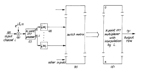
Figure 1 shows a block FFT multiplexer for variable
bandwidth inputs, and
Figures 2a to 2d show the frequency response of
filters for the multiplexer of figure 1.
The invention utilises a technique known as sub-band
decomposition and reconstruction. This technique is
described in A. Papoulis, 'Signal Analysis', McGraw-Hill,
1984; M.R. Portnoff, 'Implementation of the digital phase
-S-
vocoder using the fast Fourier transform' IEEE Trans.
Acoust., Speech, Signal Processing, vol. ASSP-24,
pp243-248, June 1976; R.E. Crochiere, 'A Weighted
Overlap-Add Method of Short-Time Fourier
Analysis/Synthesis', IEEE Trans. Acoust., Speech, Signal
Processing, vol. ASSP-28, pp 99-102, February, 1980. In
effect this is a computationally efficient implementation '
of a bank of contiguous digital filters which have
overlapping frequency responses which together span the
bandwidth of the input signal and s~.un to unit response.
This means that the individual filter outputs, or
sub-bands, can be subsequently summed to reconstruct -the
input signal. If 'the sub-band signals are decimated
(downsampled) then it is necessary to interpolate them
prior to reconstruction, which functions are efficiently
combined in an FFT multiplexer (see M.R. Portnoff,
'Implementation of the digital phase vocoder using the
fast Fourier transfornv' IEEE Trans. Acoust., Speech,
Signal Processing, vol. ASSP-24, pp243-248, June 1976,
R.E. Crochiere, 'A Weighted Overlap-Add Method of
Short-Time Fourier Analysis/Synthesis', IEEE Trans.
Acoust., Speech, Signal Processing, vol. ASSP-28, pp
99-102, February, 1980). '
The multiplexer aspect of the present invention is
shown in Figure 1. The processing stages are as shown,
namely:
-6-
1. each baseband video signal input channel (a) is mixed
with a vernier frequency correction (b)
2. each input channel is decomposed into sub-bands using
an FFT weighted overlap-add demultiplexer (c), with a
suitable filter design
3. for each channel, the sub-band outputs are decimated
(d) to the common input sampling rate of the
multiplexes
4. the sub-bands from each channel are now passed into
the appropriate ports of an FFT weighted overlap-add
multiplexes (f) by means of a switch matrix (e); the
processor (f) performs the functian of
- reconstructing the individual channels
- interpolating each channel up to the output
sampling rate B of the FDM signal
- mixing each channel up to its assigned carrier
frequency in the FDM
- multiplexi.ng the channels
The block-FFT multiplexes (f) features a K-point
complex-complex FfT transform and interpolation by a
factor L. Z'he multiplexes output (g) is a complex
baseband video signal comprising the E'DM. The individual
input channels (a) are bandlimited complex baseband video
signals. 11n input channel i is divided into Ki sub-bands
using a Ki-point FFT demultiplexer (c); each sub-band
output from the channel i. demultiplexer is decimated by a
factor Mi (d). Frequencies w (in radians/sample) in the
input channel are therefore mapped to multiplexer output
frequencies w' by the relation:
w - > w' = w Mi/L (1)
The sub-bands corresponding to channel i are spaced by
Aw = 2y('/Ki . Proper reconstruction of a channel i in the
output multiplex requires that:
L'w - > ~w' _> (2'~['/Ki) (Mi/L) - 2y~/K => K/Ki=L/Mi Z 1 (2)
Figure 2a shows the prototype frequency response of
the filter Hi(e~w) associated with sub-band decomposition
of the channel i using a Ki -po.int FFT. The ideal
response (I) is a 'brick-wall° .filter; the practical
response (P) is relaxed, with st.opband ws less than 2'~[/Ki
as shown. Note that this implies that the decimation
faction Mi associated with the sub-bands of channel i must
be less than K. .
i
Figure ~b shows the prototype frequency response of
the common filter F(e~w~) associated with the subsequent
reconstruction of the channel sub-bands and :interpolation
r~
_$_
up to the FDM output frequency in the multiplexer; the
response shown is for the particular case of interpolation
factor 1, = K/4 (practical filter designs require that h <
K ). The ideal anti-image (interpolation) filter (I)
associated with the FFT multiplexer would be 'brick-wall'
filter with passband edge at w' _ 'y~'/L = 4~(/IC. In practice
this must be relaxed as shown, with the passband edge of ,
the interpolating filter (P) at w'p =2y['/K greater than or
equal to the stopband edge of the sub-band decomposition
filter. The frequency response of the filter H.(e~w) is
shown in Figure 2b as it maps onto the output frequency
axis w' according to the relations (1) and (2.) above.
Note that:
(F(e3w~) ~ - 1 for 0 S ~w' ~ S 2y('/K (3)
This, combined with the use of a standard windowed
FIR design for the sub-band decomposition filters H.,
1
which preserves the zero-crossings of a rectangular window
in the unit sample response,satisfies the requirements for
correct reconstruction, see M.R. Portnoff, 'Implementation
of the digital phase vocoder using the fast Fourier
transform' TEEE ~!'rans. Acoust., Speech, Signal Processing,
vol. ASSP-24, pp243-248, June 1976.
The input channel i is mixed to a centre frequency:
~o~~o~~
_g_
w ~ i ~i + 29fk/K
where k is an integer o,...,K-1 and ~ a vernier frequency
offset supplied by the channel mixer (b) in Figure l,
where:
~i ~ ~9!/K
In the example being discussed the interpolation
factor in the multiplexer is L = K/4 and so the sub-bands
input to the FFT multiplexer must be at a sampling rate of
~91/L = 8~9fIK~
It can be seen from Figure 2c that an input channel i
which is bandlimited to less than ~ w' = 2y(/K (and hence '
is oversampled by at least a factor of 4) does not require
sub-band decomposition. The spectrum of channel i is
denoted as X(e~w~). Even with the maximum vernier shift
of ~ ~ ~ _ 'q('/K the shifted spectrum X (e~ (w~-~/K) ). of
i
channel i still lies entirely within -the passband of the
anti-image filter F. Such channels can therefore be
directly entered into the switch matrix bypassing
processing blocks (c) and (d) of Figure 1.
Figure 2d shows the case where an input channel i has
a bandwidth >~ w' and is subjected to a vernier shift of
~'p'/K_ 'i'he channel must be decomposed into sub-bands -to
z0~.~f~~a
avoid distortion in the transition band. of the anti-image
filter F and leakage from the images at w' _ -2~/L.
This system can be designed to accommodate a
particular mix of input channel bandwidths; with
appropriate mixing and switching of the sub-band groups to
the input ports of the multiplexer these input channels
can be multiplexed to different bands of the output FDM.
With programmable FFT processors (c) on each input line
this system offers the flexibility to be reconfigured at a
later date to accommodate a different mix of bandwidths in
the input channels.
The demultiplexer is simply the mult.iplexer run in
reverse.
The above described embodiment provides a
mathematically exact and computationally efficient
architecture with the flexibility to accommodate channels
of differing bandwidths. In particular the performance of
the multiplexer/demultiplexer in terms of its impact on
signal quality can be quantified exactly given the design
specifications on the filters used.
It will be appreciated that the above embodiment has
been described by way of example only and that many
variations are possible without departing .from t:he scope
_11_
of the invention.