Note: Descriptions are shown in the official language in which they were submitted.
HIGH MOBILITY INTEGRATED DRIVERS
FOR ACTTVE MATRIX DISPLAYS
FIELD OF THE INVENTION
The invention pertains to active matrix
displays, and particularly pertains to integrated
drivers for active matrix da.splays. More
particularly, the invention pertains to high
mobility thin film transistors for fabricating
integrated drivers for active matrix displays.
BACKGROUND OF THE INVENTION
Flat panel displays show a significant
potential for reducing the weight, volume, power
consumption, and cost, as well as providing enhanced
reliability compared to the conventional cathode ray
tube (CRT) displays. These displays are being
developed as a replacement for CRT displays in
several select applications such as for computer,
entertainment, military and anionic displays. The
display technologies, namely plasma, thin film
electroluminescence (TFEL), and active matrix liquid
crystal displays (AMLCD), which are being actively
developed to realize this potential, share the
common features of matrix addressing and the
associated driver interconnect problems. Presently,
the row and column drivers are fabricated using bulk
single crystal silicon. The driver chips are
interconnecaed to the display glass using either the
flex cable, or chip-on-glass approach. Both
approaches limit the achievable display resolution
~~9~~.~1~~
-- 2 -
due to minimum interconnect pitch required, consume
significant peripheral space, and present
reliability issues due to the thousands of
interconnects between the glass and driver chips.
By fabricating drivers on glass (integrated
drivers), the above problem;9 can be alleviated.
integrated drivers drastica:Lly reduce the number of
interconnects from several i~housand to around 10,
allow higher resolution, redundancy, and greater
flexibility in display system packaging, and improve
display reliability. Unfortunately, the present
amorphous silicon (a-Si) and polysilicon (poly-Si)
thin film transistor (TFT) technologies do not allow
fabrication of high resolution integrated drivers
due to their low mobility. A-Si has mobility in the
range of 0.1 - 1.0 centimeter2/volt*second
(Cm2/V.S.), which is too law for fabricating
integrated display drivers. Poly-Si has a mobility
in the range of 10-50 Cm2/V. Sec, and has been used
to fabricate integrated drivers for moderate
resolution displays such as 480 H x 440 V pixels.
However, for higher resolutions such as 1024 H x
1024 V, use of poly-Si TFTs requires a complex
series/parallel driver architecture, without a
dramatic reductions in the number of interconnects
required.
High resolution active matrix displays
require drivers capable of being operated in the
several megahertz frequency range. Such performance
requires a semiconductor with a field effect
mobility in excess of 300 centimeter2/volt.second.
Only single crystal silicon is known to satisfy this
requirement. Single crystal silicon allows simpler
driver architecture and dramatically reduces the
number of interconnects needs:d. However, it has not
been possible to deposit single crystal silicon
films on display glass substrates. pepending on the
substrate temperature, such depositing of silicon
films results in films that are either amorphous or
polycrystalline, and have lower mobility. Yet,
single crystal silicon films can be deposited on
sapphire substrates, i.e., silicon on sapphire (SOS)
technology, which are transparent. Although SOS
transistors have high mobility, their leakage
currents are unacceptably high for active matrix
display application. Other disadvantages are that
large area sapphire substrates are not readily
available and they are expensive.
Electrostatic bonding of a single crystal
silicon wafer to a glass substrate and thinning
(preferential etching) of the silicon wafer have
been used by others for producing high mobility
single crystal silicon films on glass substrates.
Others have utilized CORNING Code 1729 glass
substrates :in their experiments. xhe 1729 substrata
is a high temperature (i.e., strain point =
.. 4
850°Celsius (C) glass. The glass has been produced
by Corning Corp. in a small :rod form and sliced into
wafers in experimental quantities. This 1729 glass
is difficult to produce with large areas for
practical applications due to its high temperature.
The most commonly available display glass substrates
for practical applications are CORNING Code 7059,
CORNING Code 173, HOYA NA40, and ASAHI NA. The
upper useable temperature limit of these display
glass substrates is about 540°C. The difficulty is
that such temperature is not adequate for forming a
high quality thermal silicon dioxide gate dielectric
utilized in the conventional MOS processing for
display driver circuits or chips. Transistors
fabricated with deposited silicon dioxide gate
dielectric at temperatures less than 700°C,
generally have higher threshold voltages and/or
threshold voltage instabilities due to defects in
such deposited dielectric. Additionally, these thin
film transistors (TFT), when used as active matrix
switches, require light shields at the top and
bottom to anaintain low leakage currents (i.e., off-
currents), while operating under high ambient light
conditions. However, in view of the conventional
electrostatic bonding and preferential thinning
approach, it is not possible to light shield the
bottom side of the TFT because the back interface of
the substrate is not accessible after electrostatic
CA 02061796 2002-06-18
64159-1233
bonding. There is a great need for a process of fabricating
high mobility TFTs and integrated drivers, which circumvents
the above-mentioned problems. The present invention is a
process which solves those problems.
5 SUMMARY OF THE INVENTION
The present invention is a method for fabricating
high mobility TFTs and display drivers integrated on the
active. matrix substrate. Besides resulting in the single
crystal silicon for high field effect mobility, there is a
thermal silicon dioxide gate dielectric for a low and stable
threshold voltage, and light shields for low off-currents
under high ambient lighting conditions. Thus, a high
resolution active matrix display with integrated display
drivers operable in the multimegahertz frequency range, is
achievable with the present invention.
In accordance with the present invention, there is
provided a method for fabricating high mobility thin film
transistors as integrated drivers on a substrate,
comprising: growing a silicon dioxide layer on a silicon
substrate; etching the silicon dioxide layer to obtain a
plurability of gate dielectric regions of silicon dioxide;
growing a epitaxial silicon layer on the silicon substrate
and the gate dielectric regions; depositing a barrier layer
on the epitaxial silicon layer; depositing a first light
shield layer on the barrier layer; bonding a glass substrate
to the first light shield layer; etching away the silicon
substrate; etching a portion of the epitaxial silicon layer
and of the gate dielectric regions to form a plurability of
islands situated on the glass substrate, wherein each island
has the epitaxial silicon layer incorporating at least one
gate dielectric region, the barrier layer and the first
i.;,
CA 02061796 2002-06-18
64159-1233
5a
light shield layer; coating a glass layer on the islands and
exposed portions of the glass substrate on the same surface
on which the islands are situated; etching portions of the
glass layer to expose at least the gate dielectric regions
of each of the islands; depositing a polysilicon layer on
each gate dielectric region of each island; etching a
portion of the polysilicon layer and forming a polysilicon
gate situated on each gate dielectric region; implanting
source and drain implantations into the exposed barrier
layer on each island, at a thickness greater than the
thickness of the gate dielectric region; annealing the
source and drain implantations; depositing a silicon dioxide
intermetal dielectric layer on the plurability of the
islands and on remaining portions of the layer of glass;
etching contact vias through the silicon dioxide intermetal
dielectric layer to the source and drain implantations on
each island; and depositing and etching source and drain
metalizations to the source and drain implantations via the
contact vias.
In accordance with the present invention, there is
further provided a method for fabricating high mobility thin
film transistors as integrated drivers on a substrate,
comprising: growing a silicon dioxide layer on a first
silicon wafer; growing a doped silicon etch-stop layer on a
second silicon wafer; growing a silicon epitaxy layer on the
silicon etch-stop layer; bonding the first and second
silicon wafers together at the silicon dioxide layer and the
silicon epitaxy layer; etching away the second silicon
wafer; etching away the silicon etch-stop layer; depositing
a barrier layer on the silicon epitaxy layer; depositing a
first light shield layer on the silicon epitaxy first layer;
bonding a glass substrate to the first light shield layer of
i. ,
CA 02061796 2002-06-18
r.
6159-1233
5b
the first silicon wafer; etching away the first silicon
wafer; and etching regions of the silicon dioxide layer, the
silicon epitaxy layer, the barrier layer and the first light
shield layer to form a plurability of islands, situated on
the glass substrate.
In accordance with the present invention, there is
further provided a plurality of high mobility thin film
transistors as integrated drivers on a substrate,
comprising: a glass substrate; and a plurality of islands
situated a surface on said glass substrate, wherein each
island comprises: a light shield layer; a barrier layer
situated on said light shield layer; a silicon epitaxial
device layer having a first surface situated on said barrier
layer and having a second surface; a region silicon dioxide
gate dielectric embedded in the silicon epitaxial device
layer and having a surface exposed at the second surface of
said silicon epitaxial device layer; a polysilicon gate
situated on said region of silicon dioxide gate dielectric;
a plurality drain-source implantations at the second surface
of said silicon epitaxial device layer and adjacent to said
region of silicon dioxide gate dielectric, having a depth
greater than the depth of said region of silicon dioxide
gate dielectric, relative to the second surface of said
silicon epitaxial device layer; and a drain-source
metalization in contact with each drain-source implantation
of said plurality of drain-source implantations.
BRIEF DESCRIPTION OF THE DRAWINGS
Figure 1 is method flow diagram for fabricating
high mobility TFTs and an active matrix substrate having
integrated drivers.
i;
CA 02061796 2002-06-18
64159-1233
5c
Figure 2 is a cross-sectional view of a display
glass substrate and a single crystal silicon wafer prepared
for bonding.
Figure 3 is a cross-sectional view of the display
glass substrate after the bonding and thinning of the single
crystal silicon.
~~~~.~1~
-
Figure 4 is a cross--sectional view after
the silicon islands, along with the gate dielectric,
have been etched.
Figure 5 is a plan-view of the silicon
islands with the gate dielectric.
Figure 6 is a cross-sectional view of the
substrate having a spin-on-glass planarization
layer.
Figure '7 is a plan-view of the substrate
with the spin-on-glass layer.
Figure 8 shows a deposition pattern and
etch for a polysilicon gate.
Figure 9 reveals the source-drain implants.
Figure 10 shows the inner metal dielectric
deposition, pattern and etch of contact vies.
Figure 11 indicates the source and drain
metal deposition, pattern and etch.
Figure 12 reveals a passivation layer
deposition, light shield layer deposition, pattern
and etch.
Figure 13 reveals an alternate process
sequence for the first part of the process for
fabrication of high mobility ~FTs.
Figure 14 shows a preprocessed silicon
handle wafer and silicon device wafer prior to
bonding.
Figure 15 shows a cross section of the
silicon handle wafer, the thermal silicon dioxide
-
dielectric and the silicon epitaxial device layer
after the silicon device wafer and the p++ etch-stop
layer have been selectively etched away.
Figure 16 shows the preprocessed silicon
handle wafer prior to its electrostatic bonding to
the display glass substrate.
Figure 17 shows a cross section of the
display glass substrate after electrostatic bonding
and selective etching of the silicon handle wafer.
1o Figure 18 is a cross-sectional view after
the silicon islands along with the gate dielectric,
have been etched.
DESCRIPTION OF THE PREFERRED EMBODIMENT
Figure 1 shows the process flow for
fabrication of high mobility n-channel TFTs. The
process steps are described in conjunction with the
ensuing figures.
Figure 2 reveals a silicon substrate 12 and
display glass substrate 14 prior to electrostatic
bonding. Single crystal silicon substrate 12 is P-
type has a boron concentration greater than 8x10¹⁸
atoms/Cm3, a (loo) orientation, (P++) and a
thickness of approximately 0.5 millimeters. Silicon
substrate 12 is initially thermally oxidized in dry
oxygen to produce about 0.5 micron of h~.gh quality
silicon dioxide on surface 16. The thermal silicon
dioxide is then patterned and etched to produce gate
dielectric regions 18 for the TFTs to be fabricated.
g _
The pattern on the oxide also includes alignment
keys for registration of the subsequent layers to
gate dielectric regions 18. Next, approximately 1.5
microns of lightly doped epitaxial (epi) silicon 20
is grown on top of silicon wafer 12 containing oxide
islands 18. Because an Si02 layer presents a
difficult nucleation surface for silicon chemical
vapor deposition (CVD), lateral epitaxy results on
top of oxide islands 18. Thus, a uniform epitaxial
l0 layer 20 of lightly boron doped, high mobility
silican of about a 1.5 micron thickness is produced
by a selective epitaxial process. on top of layer
20, a SigN4 barrier layer 22 is deposited with a
thickness of about 0.25 micron via plasma CVD.
Barrier layer 22 serves as an isolation layer.
Silicon dioxide deposited by plasma CVD may also be
used as a barrier layer. On layer 22, a light
shield layer 24 of about 0.2 micron is deposited.
After deposition of layer 24, silicon wafer 12 is
then ready for bonding. Light shield layer 24 may
be composed of refractory metal or similar
substance, which is compatible with the
electrostatic bonding process and barrier layer 22.
Silicon wafer 12 incorporating layers 20, 22 and 24,
is then electrostatically bonded to display glass
substrate 14 at light shield 24 surface of wafer 12.
Provision For electrical contact to light shield
layer 24 for electrostatic bonding may be made by
g
any one of various means. For example, silicon
wafer 12 can be made larger than glass substrate 14
to have access to light shield layer 14, for
electrical contact during banding. Display glass
substrate 14 may be CORNING Code 1733 or other like
material. Substrate 14 is approximately 1.1
millimeters thick. Electrostatic bonding involves
applying approximately 1000 volts direct current
across the display glass substrate 14 and wafer 12
for a bonding between layers 14 and 24 at a
temperature of about 600°C.
After the bonding of layers 14 and 24, p++
silicon substrate 12 is etched off starting from the
surface opposite of surface 16, down past surface 16
on into layer 20, including some of islands 18 to a
level wherein a portion of thickness of islands 18
is remaining. This etching is accomplished with the
use of impurity selective etch 8FiAc:3HN03:1HF.
Impurity selective etch preferentially etches the
P++ silicon layer 12 one hundred times faster than
the lightly doped epi-silicon layer 20. This
permits a controllable etch removal of P++ substrate
12. Alternatively, a majority of the silicon wafer
12 may be removed by mechanical grinding and lapping
prior to impurity selective preferential etching,
for the remainder of wafer 12. A portion of epi
layer 20 and thermal oxide islands 18 are
controllably etched to achieve about 1,000 angstroms
- 10 -
of gate dielectric 18 as shown in Figure 3. This
etching can be dons using wet chemical etching or
plasma etching.
Silicon epi layer 20, barrier layer 22 and
light shield 24 are patterned and etched to form
islands 26 for the fabrication of TFTs for the
active matrix array and display drivers, as shown in
Figures 4 and 5.
Spin-on-glass 28 (e. g., Allied Chemical
ACCUGLASS XA03-5) is applied on substrate 14 and
islands 26, and is patterned and etched as shown in
Figures 6 and 7. Spin-on-glass 28 protects the
subsequent gate 30 from shorting to the TFT channel.
Also, spin-on-glass 28 planarizes the surface.
Then a polysilicon gate 30 is deposited,
patterned and etched as shown in Figure 8. This is
followed by self-aligned source-drain implantation
32 of phosphorus (P31), and anneal as shown in
Figure 9. The implant 32 damage is annealed at 600
C. in a furnace for 20 hours. Tmplant 32 conditions
are selected to achieve an implant 32 range greater
than the thickness of gate oxide 18. Then a silicon
dioxide intermetal dielectric 34 is deposited by
plasma chemical vapor deposition, patterned and the
contact vies are etched down to implants 32, as
shown in Figure 10.
Aluminum (+1% Silicon) is then deposited,
patterned, and etched to define the source-drain
11 -
metalization 36 as shown in Figure 11. This
completes the fabrication of TFT 40 for active
matrix and integrated drivers. The next step is to
fabricate a pixel electrode that electrically
connects to the source electrode of -the active
matrix pixel TFT. For AMLCL)s, an Indium Tin Oxide
(ITO) layer, which is a transparent conductor, is
deposited, patterned and etched to define the pixel
electrode. For clarity, the: pixel electrode is not
shown in Figures 11 and 12. To maintain low leakage
currents under high ambient lighting conditions,
another light shie~.d 44 is placed on the top of the
TFT. First a silicon dioxide passivation dielectric
layer 42 is deposited on top of source-drain
metalization 36. Then a second aluminum layer is
deposited, patterned, and etched to obtain top light
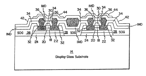
shield 44 as shown in Figure 12.
This active matrix substrate with high
mobility TFTs and integrated drivers is then
utilized to fabricate high resolution AMLCDs using
conventional liquid crystal display assembly
techniques.
Note that the invention can also be used to
fabricate integrated drivers only using the high
mobility single crystal silicon TFTs, while using an
a-Si or po:Ly-Si TFT array for an active matrix.
Further, the high mobility TFTs of this invention
can be used to fabricate integrated drivers for TFFL
- x2 -
and plasma display panels, Additionally, the high
mobility TFTs of this invention can be used to
fabricate active matrix TFEL displays with
integrated drivers. In the case of an active matrix
TFEL display, a reflective :film such as aluminum is
used as the pixel electrode. The source-drain
aluminum (see Figure 11) is used to fabricate the
reflective electrode for the electroluminescent
pixel.
The high mobility TFT process described
above illustrates the procedures for fabricating n-
channel TFTs. If p-channel TFTs are required, a
similar process can be employed by changing the
dopant in film 20 to phosphorus, and the source-
drain implant 32 in Figure 11 to Boronll (B11).
Also, complimentary metal oxide semiconductor (CbinS)
devices, involving both n-, and p-channel TFTs on
the same substrate, can be fabricated by masked
implantation of the selected TFT locations (gate
dielectric regions) with P31 or B11 after selective
epitaxial deposition to create n- and p-regions,
prior to electrostatic bonding. Display drivers
using CMOS circuitry consume less power.
Figure 13 shows a flow diagram for an
alternate processing scheme for fabricating high
mobility single crystal silicon TFTs on a display
glass substrate 4~ using a high quality thermal
~~~~.~1~~
- 13 -
silicon dioxide gate dielectric 48. This approach
is shown in figures 14-18.
This process uses 'two single crystal
sil~.con wafers, labelled as a silicon device wafer
50 and a silicon handle wafer 52, respectively.
Both wafers 50 and 52 are o:E p-type with resistivity
of about 1 ohm-cm, and (100) orientation. First, a
high quality thermal silicon dioxide layer 48 of
about a 5000 angstrom thickness is grown on wafer 52
using dry oxygen at a temperature of about 1000
degrees C. Tn parallel, a heavily boron doped p++
silicon etch-stop layer 54 with a thickness of about
2 microns, and a lightly doped (p- or n-) device
layer 56 with a thickness of about Z micron are
grown on silicon device wafer 50, using silicon
epitaxy. Then the two wafers,50 and 52, are bonded
to each other either by using electrostatic bonding
or diffusion bonding. Figure 14 shows a cross-
section through silicon handle wafer 52 and silicon
device wafer 50 prior to bonding. After bonding,
silicon device wafer 50 is selectively etched away
using selective chemical etch such as ethylene
diamine pyrocatechol (EDP). Figure 15 shows a
cross-section through. handle wafer 52 after the
bonding and selective etching of device wafer 50.
Then, silicon handle wafer 52 is
photolithographically patterned to etch alignment
keys in silicon epi device layer 56 and thermal
2~~~.~~~~
- 14 -
silicon dioxide gate dielectric 48. This allows
masked implantation anneal of the n- and p- regions v
in device epi silicon film 56 prior to bonding to
low temperature display glass substrate 46. (The
alignment key fabrication and corresponding masked
implantation processes are not shown.)
Next, a barrier layer 58 (about a 2500
angstrom think ,plasma deposited silicon nitrite or
silicon dioxide), and light shield layer 60 of about
2000 angstroms thick are deposited on top of silicon
epi device layer 56 as shown in Figure 16. This
pre-processed silicon handle wafer 52 is then
electrostatically bonded to display glass substrate
46 at light shield layer 60. After bonding, silicon
handle wafer 52 is selectively etched away using the
EDp etch or potassium hydroxide (KOH) etch. Etch
rate of these etches for the thermal silicon dioxide
dielectric is insignificant compared to the etch
rate for handle silicon wafer 52. Figure 17 shows a
cross-section through display glass substrate 46 and
accompanying layers 48, 56, 58 and 60, after silicon
handle wafer 5,2 is selectively etched away. Then,
silicon islands 62 along with thermal silicon
dioxide dielectric layer 48, are patterned for the
regions requiring TFTs, and etched as shown in
Figure 18. From this point on, the substrate
assembly in Figure 18 is processed similar to the
first approach starting from Figure 5. The
-- 15 _
corresponding components of devices 64 and 66 are,
respectively, glass substrates 14 and 46, light
shield layers 24 and 60, barrier layers 22 and 58,
silicon epitaxial layers 20 and 56, silicon dioxide
dielectrics 18 and 48, and :islands 26 and 62.
In summary, the invention permits
fabrication of TFTs having saingle crystal silicon
for high mobility integrateci drivers for active
matrix displays wherein high mobility means that in
excess of 300 Cm2/V.S., thermal silicon diaxide gate
dielectric for low (less than 1 volt) and stable
threshold voltage, and light shield for low off--
currents (less than 1 pico ampere) under high
ambient lighting conditions are accomplished.
The present invention may utilize
variations to the basic processes, illustrated
above, such as by using different thicJtnesses for
individual layers, processing temperatures, and
other processing conditions.