Note: Descriptions are shown in the official language in which they were submitted.
2~21~3 ~
, ,
SZ 9-91-002
SEMICONDUCTOR DEV~CE COMPRISING A LAYERED STRUCTURE GROWN
ON A STRUCTURED SUBSTRATE
TECllNICAL FIELD
The invention concerns semiconductor devices such as laser diodes
comprising layered structures grown on a structured substrate having horizontal
surface regions with adjacent inclined sidewall facets. The invention is
particularly well suited for visible wavelength laser diodes with an active layer
consisting of a compound semiconductor (III/V or other). The active layer can be~terminated in any lateral directinn with wider bandgap rnaterial whereby burieddevices providing for strong confinement and non-absarbing mirror structures
can be obtained.
BA~ICGROUND OF THE INVENTION
One of the major applications of the present invention is in the field of
semiconductor laser diodes which are now being used in a wide variety of
information handling systems because of their compact size and because their
technology is compatible with that of associated electronic circuitry. These lasers
are being used in areas such as data c:ommunication, optical storage and laser
beam printing and haw been optimi;~ed for the particular applications with
regard to their wavelength, optical power, their high speed modulation
capabilities, beam quality, etc.
The invention herein described, though applicable to a rather broad spectrum of
different devices, is of particular interest for short wavelength lasers employed
e.g. in laser printers and optical disk systems requiring narrow beams at high
optical power. Very attractive 1or such applications are (Al)GalnP laser diodes
operating in the 0.6~m ~avelength range. These short wavelength materials,
however, have characteristics that are different fro~i those of the widely
20~2~3
2 SZ 9-91-002
investigated and used- (Al)GaAs material syst~r~s`arid th`at lead to additional
problems. In other words concepts~and designs adequate for (Al)GaAs devices
are not generally suitable for visible light lasers~
The present invention provides for solutions to two of 1he key requirements
namely
-- strong current and carrier confinement to obtain low threshold highly efficient
laser diodes and
-- protection against catastrophic optical mirror damage (COMD) occuring due
to heat developing at the mirror facets to permit high output power operation
- for long device~lifetimes,~ r
Substantial improvements with regard to carrier and current confinement have
already been achieved with so-called buried structures wherein the active layer
of the laser is embedded in wider bandgap material in the direction parallel to
the waveguide forming the Taser càvity~ However known structures require
raSher complex fabrication processes. Most commonly used is a process starting
with an etch step to obtain a mesa including the GalnP active layer. The mesa isthen buried using a sequence of epitaxial regrowth steps. This technology is notonly accompanied by a strong loss in device yield but moereover can also cause
severe devlce reliability problems.
~,",
Another example of a buried structure and its fabrication process have been
dlsclosed in the published European Patent Application 0 348 540 Process for
the selective Growth of GaAs . Here a patterned substrate with horizontal and
, .. .
inclined surface sections of different crystal orientation is used to provide for
selective growth of the active layer on horizontal surfaces whereas the
embedding wider bandgap cladding layers grow on both the horizontal and the
inclined surfaces. Like other methods that rely on crystal orientation dependentno- or reduced-growth effects this process is problematic in that during the
epitaxy process no- or reduced-growth unprotected facets may be contaminated
the crystal structure affected.
- --
~ O ~ r~ 3
3 SZ 9-91-002
Great efforts have also been invested In the deslgn of laser structures having
non-absorbing mirrors (NAM) to avoid excessive heating due to non-radiative
carrier recombination near the mirror facets. Here, the general approach is to
terminate the active layer with a so-called window structure consisting of
transparent, wider bandgap material thereby substantiall`y reducing the number
of carrier pairs near the facet. Such NAM laser structures have been disclosed in
the following documents;
-- Article "Non-Absorbing Laser Mirrors", published in IBM's Technical
Disclosure Bulletin, Vol. 31, No.2, July 1988, p. 240. Described is an (Al)GaAs
laser consisting of a layered structure comprising an active GaAs quantum
well layer embedded between cladding layers. The layers are grown on the
structured surface of a GaAs substrate: the center portion on a (100)-plane,
both mirror regions on (411)-planes. Since the GaAs growth speed is
remarkably lower on the (411)-surfaces, the width of the active quantum well
Jayer is reduced near the ~nirror,,regions. This results in an increase in
effective bandgap.
i .... . . .. ... . .
European Patent Application 0 332 723 "High-Powel- Semiconductor Diode
Laser" shows a laser structure formed on a patterned substrate having planar
mesa- and groove-sections with inclined transition zones inbetween. The
layered structure comprises an active and a passive waveguide, the gain
segment of the active waveguide being aligned with the non-absorbing section
of the passive waveguide. Light generated in the gain section is coupled
through an inclined cladding layer into the non-absorbing section where it is
fully guided when propagating towards the mirror facets.
Article "Vertically Emitting Laser with integrated NAM deflector", published in
IBM's Technical Disclosure Bulletin, Vol.32, No.3B, August 1989, pp.498/499,
proposes other forms of non-absorbing mirror or deflector structures. In one
instance, the active layer, made of quantum wells, is disordered by ion
implantation or diffusion. This !ocal disordering rises the bandgap of the
active layer. In another embodiment, the active layer is bent just before the
deflector. The light beam impinges on the deflector in its non-absorbing part
formed by a wider bandgap cladding layer.
2~ 21~i3
4 SZ 9-g1-002
-- Article "Novel Window-Structure AlGalnP visible LDs with non-absorbingFacets formed by disordering of natural Superlattice in GalnP Active Layer",
by Y~Ueno et al, published in Conference Digest 12th IEEE International
~ Semicon~luctor Laser Conference, I:)avos/Switzerland, September 1990,
pp.30/31. A visible light AlGalnP laser diode is described that has a higher
bandgap (Eg) crystal incorporated at the mirror facets. This is accomplished by
selective disordering the GalnP active layer with diffused impurity (Zn) near
the facets whereby E9 is increased. A marked increase in maximum light
output power is demonstrated.
-- Article "Window-Structure InGaAlP Visible Light Laser Diodes by
Self-Selective Diffusion-lnduced Disordering" by K. Itaya et al, published in
the same Conference Digest as the previous reference (on pages 36 1 37).
Again, Zn-diffusion-induced disordering is used to create a wider bandgap
window region for an InGaAlP laser structure. The diffusion is obtained below
an n-cap layer selectively left in the mirror region.
These known NAM concepts require rather complex structures and fabrication
processes and there is a demand for higher yield, "easy-to-make" NAM laser
diodes.
The invention hereinafter described allows the design of laser devices where
strong current and carrier confinement as well as NAM waveguides can be
realized within a single epitaxial step. This is achieved through local bandgap
variation by simultaneous in-situ growth of group lll ordered phase and
disordered phase semiconductor material on a structured substrate.
The invention is based on the phenomenon that some semiconductor materials,
especially (Al)GalnP which becomes very important for visible light laser
applications, have been found
-- to exist in several phases, i.e., ordered and disordered, which differ in the atomic arrangement of group lll species,
2~.~2~
SZ ~91-002
to have a bandgap energy Eo that increases when changing from the ordered
to the disordered phase, and
-- fo grow under standard Metal Organic Vapor Phase Epitaxy (MOVPE) gro~th
conditions in the ordered phase on a standard substrate orientation (or on a
slightly misoriented surface) whereas, in case of stronger misoriented
substrates, the disordered phase is obtained.
These material characteristics have been investigated and reported on in the
following articles:
-- "Evidence for the Existence of an ordered State in GalnP grown by Metal
Organic Vapor Phase iEpi1axy and its P~elation to Band-Gap- Energy", by
A.Gomyo et al, published in Appl.Phys.Lett. 50(11), 16 March 1987, pp.673-675.
It is demonstrated that MOVPE epitaxial layers can, depending on III/V ratios
and growth temperaturesj assume states of different bandgap energy (Eg)
corresponding to an ordered and to a random (Ga,ln) distribution on column
lll sublattices.
-- "Dependence of Photoluminescence Peak Energy of MOVPE-grown AlGalnP onSubstrate Orientation", by S.Minagawa et al, published in Electronic Letters,
8th June 1989, Vol.25, No.12, pp.758/759. This is a report on measurements of
GalnP and AlGalnP materials grown by MOVPE. It has been found that the
bandgap increases as the substrate misorientation with respect to the
(100)-plane increases and that it saturates at high inclination angles due to
-- complete transformation into random alloy.
These articles describe the material properties on which the present invention is
based but do neither suggest the use of structured substrates to selectively
obtain regions of different bandgap, nor do they propose the application of the
investigated phenomena to achieve buried heterostructures and/or
non-absorbing mirror facets in diode laser technology.
2 0 ~ 3
6 SZ 9-91-002
- ^ SUMMARY OF THE INVENTION ~ i
A main object o~ the present invention is to provide a semiconductor d~vicet
with improved current and carrier confinement characteristics that can- be
fabricated using conventional, easy-to-control processes.
Another main object is to provide a semiconductor device such as a laser diode
having an active waveguide with essentially non-absorbing mirror sections that
can be fabricated using a one-step epitaxy process.
A further object is to provide a semiconductor device comprising an active
waveguide having sections of wide bandgap material in both lateral directions toimprove carrier confinement and to obtain non-absorbing mirrors.
, ~ . ... . .. .
Still another Qbject isi to provide .a semiconductor device such as a laser diode
and a method for its fabrication, the device having an active layer comprising
sections of different bandgap energies, wherein the active layer can be fabricated
in-situ in a single process step.
The invention as claimed herein is intended to meet these objectives and to
remedy the deficiencies of known semiconductor devices, particularly of laser
diodes. This is accomplished in that the layered structure forming the device isgrown on a structured substrate. At least the active layer is of a semiconductormaterial that assumes ordered or disordered states as a function of the substrate
surface orientation or misorientation, these states having different bandgap
energies E9. Bent terminating sections of the active layer, grown on misorientedsubstrate surface portions, provide for a bandgap energy higher than that of thecenter section and thus allow the fabrication of buried lasers and/or of active
Iayers terminated with a wide bandgap section which, in laser diode applications,
provides for non-absorbing mirrors.
The active layer, comprising high and low bandgap regions, can be fabricated
in-situ, i.e., in a single epitaxy process step.
2~ 21 ~3
7 SZ 9-91-002
The main advantages offe-red hy th~ inventlon can be summarized as foilows:
The buried heterostructure device provides, in laser applications, for
tmproved confinement, andlor for non-absorbing mirrors protecting the device
against catas1rophic optical mirror damage, and can be fabricated using
non-critical conventional epitaxy processes;
Improved laser performance with respect to threshold current values,
efficiency, reliability and optical output power can be achieved;
Planar technology processes can be employed because the relied-upon effect
requires only small inclination angles-at the substrate surface, and the in-situepitaxial deposition process reduces critical alignment requirements to a
minimum; and .. ~ .-.... ..
The use of shallow,i inclined..facets .avoids material. redistribution and
differences in reaction rates that, otherwise, cause local changes in
composition and result in strain or in the formation of defects.
DESCRIPTION OF THE DRAWINGS
Different ways of implementing the invention are described in detail below
: with reference to drawings which illustrate specific embodiments and in which
" ~ .
Fi~. 1 shows, for two laser diodes deposited during the same growth run
but on substrates of different surface misorientation, how the
bandgap energy and ~hus the emission wavelength is affected.
Fi~. 2A/2B are schematic views of layered ridge (A) and groove (B) structures
that are used to illustrate the phenomenon on which the invention is
based .
2 ~
8 SZ 9-91-002
F~g. 3 is a perspective view of a first embodiment of- the invention; shown
is a groove-type laser diode having a buried active layer for
achieving effective confinement. - - ~ '~ I~
.. .. ... ~,
Fig. 4 is a perspective view of a second embodiment of the invention;
shown is a groove-type laser diode having non-absorbing mirror
sections in order to avoid catastrophic optical damage.
Fi~. 5 is a perspective view of a third embodiment of the invention; shown
is a groove-type laser diode having both, a buried active layer and
non-absorbing mirror sections, thereby providing for effective
confinement and for high power output by avoiding catastrophic
- optical damage caused by heat developing at-the mirrors.
~ETAILED DESCRIPTION
Before describing the embodiments of the inventive semiconductor device in
greater detail, the basic principles on which the invention is based will be
outlined with the aid of Fig. 1 and 2A / 2B.
Some III/V compound semiconductor materials, especially (Al)GalnP, can exist in
different phases which differ in the atomic arrangement of group lll species.
Depending on the conditions during growth, e.g. in a Metal Organic Vapor Phase
Epitaxy (MOVPE) process, a random or disordered alloy phase, or an ordered
phase, where Ga and In atoms are regularly arranged, e.g. in the < 111 >
direction, is obtained. The most interesting difference between the two phases is
that the bandgap energy Eg of the same material is, in the disordered phase, 70
to 150 meV higher than in the ordered phase. Whether the semiconductor
material will grow in the ordered or in the disordered phase, can be determined
by the orientation of the substrate on which it is grown. Under typical MOVPE
growth conditions, yielding high optical quality materials, GalnP grows in the
ordered phase on standard substrate orientations like (100) or slightly
off-orientations (e.g. 2), whereas it will grow in the disordered, random alloy
-
20~21~3
g SZ ~91-002
phase on a stronger misoriented s~lbstrate! a~ rather low o~f-angle of ~.~;7
already being sufficient.
.
Fig.1 shows emission spectra of two lasers (of the GalnP MQW GRINSCH type)
grown simultaneously side by side on (100) 2 off =~ (110) and 7 off =~
<111~A GaAs substrates respectively. The emission wavelengths of the two
lasers have been measured as 673 nm and 654 nm for the 2 off and the 7 off
substrate orientations respectively the difference in wavelength being caused bythe difference in bandgap energy. The composition of the alloys deposited on thetwo substrates has been measured and determined to vary by less than 1 %
thus verifying that sto~chiometric incorporation is obtained despite the small
inclination difference.
It has now been found that local bandgap variations can also be obtained within
a layer or layered structure that is grown on a single structured substrate having
surface regions of different misorientation. ~ -
Thls is illustrated in Fig.2A show~ng schemat~cally a simple structure comprisinga structured substrate onto which an (Al)GalnP-layer is grown. The substrate
designated 11 may consist of (100)-oriented GaAs. As shown it is structured to
form a shallow ridge providing horizontal mesa (a) and groove (b) regions that
are (100j-oriented or only sli~htly misoriented as well as inclined transition
regions (c) of stronger misorientation. Grown on this structured surface is a layer
12 of (Al)GalnP i.e. a III/V compound semiconductor material that can exist in
oither the ordered or in the disordered phase. On the oriented (or slightly
mlsorlented) horizontal surface regions (a b) the ~AI)GalnP layer is in its ordered
phase wlth a bandgap correspondlng to an emission wavelength of about 670 nm
whereas In the Inclined regions (c) of stronger misorientation the material is
disordered the bandgap corresponding to an emission wavelength of about 650
nm. This is illustrated in the figure: sections 12a and 12b of (Al~GalnP layer 12
grown on orlented substrate surfaces a and b consist of ordered material
whereas sections 12c (shaded areas) grown on misoriented substrate surfaces c
are of the disordered type.
2~3i3?,1~3
SZ ~91-002
The changes in bandgap energy-Eg that occur at the ordered-disordered material
interfaces are schematically illustrated in the energy (E) diagrams of the
conduction band (Ec) and the valence band (Ev) shown below the structure. The
aifference between the energy gaps Egd,s (for the disordered material) and Ego,d(for the ordered material), has been found to be in the range 70 to 150 meV.
Fig.2B is an illustration of a groove-structure showing the same effect: layer 12,
grown on the structured surface of substrate 11, comprises ordered and
disordered regions as in the tidge structure of Fig.2A, resulting in the same
energy diagram.
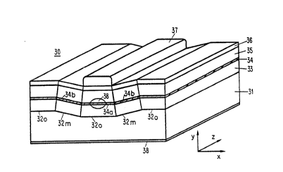
Fig.3 is a perspective view of a first embodiment of a semiconductor device
designed and fabricated in accordance with the present invention, the
embodiment being a laser diode structure 30 providing for improved lateral
current and carrier confinement.
.. . ., . ., ", . - , . " ;, .. . ...
Basically, laser 30 is a groove-type structure grown on an n-doped GaAs
substrate 31 having a structured surface. The substrate surface comprises
horizontal regions 32O with inclined transition regions or sidewall facets 32m
inbetween. The shallow groove formed at the substrate surface is in the direction
of the light emitting waveguide of the laser structure (in Fig.3 parallel to thez-coordinate). Grown on the structured surface is a stack of semiconductor
layers. In the embodiment, this consists of an n-doped AlGalnP lower cladding
layer 33, the acfive, undoped GalnP layer 34 for carrier recombination and lightguiding, a p-doped AlGalnP upper cladding layer 35, and a highly doped, low
resistance p-GaAs contact layer 36. Ohmic contacts 37 and 38 are arranged as
shown on top of the contact layer 36 and at the bottom of the substrate 31,
respectively. At both ends of tlhe layered structure, mirror facets (in x-y planes)
are formed, their distance determining the length of the laser cavity.
When applying a voltage of sufficient level and proper polarity to the ohmic
contacts to feed a curren~ through the device that exceeds the threshold current,
a laser beam parallel to the plane of the active layer 34 is emitted from light
mode region 38.
2~21 ~3
11 SZ ~91-002
In accordance with the invention, the horizontal surface regions 32O are
"oriented", the orientation being determined by the substrate- used, in the
example a standard (100)-oriented GaAs substrate. In contrast thereto, the
inclined regions 32m are misoriented, the inclination angle being 7. Due-to-theabove explained phenomena, causing certain materials to grow in the disordered
phase on misoriented surfaces, the (Al)GalnP sections over the inclined sidewallfacets 32m (in the figure shown as shaded areas) are of a material having a
higher bandgap than that of the sections grown over oriented substrate surface
regions 32O.
As a result, section 34a of the active layer, in which the recombination proceeds
and the laser beam is generated, is laterally buried by terminating sections 34bof higher bandgap material that provide for excellent current- and carrier
confinement. The bend in the layer provides, in addition, for good lateral optical
confinement. If desired, stronger confinement can be achieved by stronger
bending of the active layer.
Now, the fabrication process for the laser structure 30 of Fig.3 will be outlined.
.
Starting point is a standard (100)-oriented n-doped GaAs substrate having an Si
doping concentration of Z x 10'acm-3. Next, the shallow grooves are prepared on
the substrate surface using standard lithography and etching techniques. First,
photoresist stripes parallel to the z-axis are formed to define the groove, the
~roove then being formed in a wet chemical etch process, using e.g., a mixture of
H2SO4, H2O2, and water. Underetching causes the formation of the desired
Incllned sldewall facets. In the embodiment, the groove of the structured surface
Is about 0.5 ~m deep and at the bottom (horizontal region 32O) 6~um wide; regions
32m are about 4 ~llm long, the inclination about 7.
After removal of the photo resist stripes, the substrate is loaded into an MOVPEsystem where the following layers are epitaxially grown in a singlc in-situ
process:
- n-doped lower claddin~ layer 33 of (AIxGa(, x~)05ln0sp with an Al-concentra1ion
x = 0.8, 1 ,llm thick and with an Si-doping of 1 x 10'3cm-3
- - \
20~2~ ~3
12 SZ 9-91-002
-- undoped active layer 34 of Ga0sln0sp~ approx.-100 nm thick; - - ; r
- p-doped upper cladding layer 35 of (AIxGa(,_x))0sln0sp with an Al-concen1ration
x = 0.8, 1 ,llm thick and with an Zn-doping of 1 x 10 ~cm-3 and - ^ ~^
, . . . . , . , , . . -
-- p-doped contact layer 3fi of GaAs, 200 nm thick and with a Zn-doping of
.1x10~9cm-3. .
In a next~ step, ohmic contact stripes 37 are applied on top of the GaAs contact~layer 36. The stripe geometry of the contact is determined and formed using a
litho9raphically patterned photoresist mask for the evaporation of the contact
metal which may consist of- a titanium/pla1inumtgold sandwich, this being
followed by a lift-off process. Ohmic contact 38 at the bottom side of 1he n-doped
substrate 31 is obtained by alloying germanium, gold and nickel. Finally, the
substrate is cleaved to form the mirror facets and to separate the devices.
,~ , .
Fig.4 is a perspective view of a second embodimemt of the invention. Shown is a
laser diode 40 with non-absorbing-mirror (NAMjsections allowing for high-power
operation. A very simple gain-guided laser structure is chosen since it appears to
be best suited for the explanation of the present invention.
Basically, laser 40 is of a structure similar to that of Fig.3, the main difference
being that the groove is formed in the x-direction, i.e., it is perpendicular to the
emitting waveguide of the device.
Laser 40 is grown on an n-doped GaAs substrate 41 having a structured surface
w7th horizontal region 42O and, at both ends thereof, inclined terminating regions
42m. The shallow groove so formed is perpendicular to the waveguide of the
laser structure. Grown on the substrate is a stack of semiconductor layers,
comprising an n-doped AlGalnP lower cladding layer 43, undoped GalnP active
layer 44, upper p-doped AlGalnP cladding layer 45, and a p-doped contact layer
46. Ohmic contacts 47 and 48 are applied as shown on the top of the contact
layer 46 and to the bo1tom of the substrate 41. Mirror facets, in x-y planes, are
formed at both ends of the layered structure.
.
,
2 ~ 3
13 SZ 9-91-002
In accordance with the invention, the horizontal surface region 42O is "oriented",
e.g. (100), whereas the inclined regions 42m are misoriented, e.g., 7 off. As aresult, the sections of the semiconductor layers grown onto the oriented
substrate substrate region 42`o are in the ordered phase, whereas the sections
above the misoriented, inclined surfaces 42m are in the disordered phase. Since
the (Al)GalnP semiconductor material grows in the disordered, higher bandgap
phase on misoriented surfaces, the semiconductor sections over the inclined
sidewall facets 42m (in Fig.4 shown as shaded) consist of material having a
higher bandgap energy than the sections grown over oriented substrate surface
420.
As a result, gain section 44a of the active layer in which the laser beam is
generated, is terminated at both~ mirror ends with higher bandgap sections 44b
providing a window or NAM portion through which the laser light is emitted. Due
to the high bandgap termination of the active layer, the number of carrier pairs in
the mirror section is greatly reduced whereby non-radiative carrier
recombination and the resulting heat development are avoided. The light beam
~follows" the bended active layer, leaving the device at light mode region 48.
The process employed to fabricate the laser of Fig.3, can be used substantially
unchanged and with the same materials, dimensions, doping concentration, etc.,
for the fabrication of the device shown in Fig.4. Of course, the groove
dimensions and its orientation with respect to the active waveguide need to be
adjusted. The inclination angle and the length of the inclined, misoriented surface
re~ions may be kept the same but the width of the groove has to be increased (toe.g. 250 to 300,1~m) and adjusted to obtain the desired cavity length of the laser.
., .
Fig.5 shows a simplified schematic view of a third embodiment of the invention. It
illustrates a laser diode 50 having higher bandgap sections terminating the active
layer in both lateral directions whereby devices with good confinement AND with
non-absorbing mirrors, providing for high output power, can be obtained.
Basically, the laser 50 consists, like the devices illustrated in Fig.3 and 4, of a
stack of layers grown on the structured surface of a substrate 51. The stack
includes a lower cladding layer 54, an active layer 55, and an upper cladding
2~21~3
14 SZ ~91-002
layer-56. For simplicity reasons,~the contact layerT deposited on top of-cladding
layer 56, and the ohmic contacts attached to the- contact layer and to the
substrate are not shown. - ~
The structure differs from those of Fig.3 and 4 in that the substrate surface and
thus the epitaxially grown semiconductor layers form grooves not only in one
direction (z or x) as in the previously described embodiments but in two
directions: parallel to the active waveguide in the z-direction and, perpendicular
thereto, in the x-direction.
This is accomplished by more complex structuring of the substrate surface. In the
z-direction, the surface has horizontal, oriented surface regions 520 with inclined,
misoriented regions 52m inbetween, whereas, in the x-direction, the surface has
horizontal regions 530, oriented where in line with the horizontal regions 520,
and inclined- and misoriented regions 53m. In Fig.5, those sections of the
different semiconductor layers-that are grown on inclined substrate surfaces andthus of higher bandgap energy are emphasised, appearing as shaded areas.
The completed device 50 of Fig.5, when fabricated h~ accordance with the
processes described above in connection with the first two embodiments,
combines the features and effects achieved with the earlier desribed devices in
that it provides for strong carrier confinement and for a NAM structure.
, -- .
With reference to the embodiments herein described, it has been shown that by
choosing a suitable arrangement of the grooves and the mirror facets, lasers with
lateral current confinement as well as lasers with non-absorbing mirrors, and
-~ even a combination of both, can be achieved.
~ -
The disclosed embodiments are groove-type devices but it should be noted tha1
the same results can be obtained using other devices such as ridge-type devices
when their design is based on the same concept and fabricated using the
processes herein described essentially unmodified.
The invention is not only applicable to laser diodes. It will also lead to
improvements in other semiconductor devices where the structure provides for
2~2153
SZ ~91-002
bandgap-controlled carrier confinement. The invention could be of particular
interest for bipolar devices.
In general, the invention is by no means limited to devices and processes using
the particular materials, dimensions, doping concentration or process parametersused for the above described embodiments. To name just a few deviations or
alternatives:
-- The invention may be applied in compound systems other than (Al)GalnP. III/V
or Il/VI compounds, ternary, quaternary, etc., are candidates provided the
material can exist in two distinct phases, which differ in the atomic
arrangement and in band energy.
In the described embodiments, the substrates used were of a standard
orientation such as (100), allowing normal epitaxial growth. Substrates of
;~ ~different orientation may also be used provided they allow proper growth with
the employed epitaxy process.
-- Instead of using an "exactly oriented" substrate such as (100), a slightly "off"
oriented substrate surface may also be used. This can be advantageous in
that it provides for defined nucleus serving as basis for crystal growth. High
quality devices can be grown on slightly misoriented, e.g., 2 off, surfaces.
Different misorientation directions are feasible, directions (110) and (111)
- being examples.
~. . .
The required misoriented substrate surfaces on which disordered material is
to grow, may be obtained with inclination angles other than the above
described 7. In fact, structures with angles of about 25 which are easier to
make, have been successfully tested. For even larger angles, limitations are
to be expected. They may lead to changes in material composition as
described above, or may deteriorate the waveguide function. In addition, the
advantageous planar lechnology may not be applicable anymore.
... ...
2~21~3
1 6 SZ 9-91 -002
-- A preferred process for fabric2lting the inventlve device is the MOVPE, but
other epitaxy processes will be suitable as well provided the atomic ordering
effect on which the invention is based can be achieved.
.
-- In fabricating !he inventive structure, a cleavage process for forming the
mirror facets and for separating the devices grown on the substrate can be
used as indicated above. O~her methods such as etch processes, particularly
Reactive lon Etch (RIE) techniques, may equally well be used to form the
mirror facets.
: - :
. . .
,', : .
'''- '
i :, .
.'~' ' , .
.