Note: Descriptions are shown in the official language in which they were submitted.
2062230
This invention relates to an electrophotographic
printing apparatus capable of printing images by
electrophotographic processing and a method of starting
up this apparatus.
Electrophotographic printing apparatuses print an
image by processing a single photosensitive object
primarily through charging, exposure, development, and
transfer, which constitute an important part of
electrophotographic processing.
Electrophotographic printing apparatuses generally
use a photosensitive drum as a photosensitive object.
Along the periphery of this photosensitive drum, a
charging device, an exposure device, a development
device, and a transfer device are arranged sequentially
to complete the printing apparatus.
In the electrophotographic printing apparatus with
this arrangement, the photosensitive drum undergoes a
particular process, passing under each device, with the
result that it is subjected to a series of electropho-
tographic processes while making a turn. Specifically,
the charging device charges the surface of the
photosensitive drum (the photosensitive surface) to, for
example, -500v. Then, the exposure device exposes the
charged photosensitive surface according to an image to
be printed. As a result of this, an electrostatic
latent image is formed on the photosensitive surface of
the drum. The development device develops this
206~231)
electrostatic image as follows, for example. A
cylindrical development sleeve holds charged toner of
the same polarity as that of the charged potential of
the photosensitive drum, and permits the toner to come
into contact with the photosensitive surface of the drum
as it rotates. Here, by applying a development bias to
the development sleeve, the bias being of the same
polarity as that of the charged potential of the
photosensitive drum and lower in voltage (for example,
-200V), the interaction between the electrostatic image
and the development bias allows the toner to selectively
adhere to the photosensitive drum. That is, toner does
not adhere to the charged portions on the drum because
the drum is at a higher potential, whereas it adheres to
the exposure-discharged portions because the drum is at
a lower potential. As a result, a toner image is formed
on the photosensitive surface of the drum.
Then, printing paper is placed on the
photosensitive surface of the drum. The transfer device
supplies to the printing paper charges of the opposite
polarity to that of the toner (for example, +500v). As
a consequence, the toner attaching to the photosensitive
surface of the drum adheres to the printing paper,
causing the toner image to be transferred to the paper.
After this, the cleaning device removes the residual
toner from the surface of the photosensitive drum.
When the electrophotographic printing apparatus
~ 2062230
thus constructed is not in operation, the potential of
the surface of the photosensitive drum is indefinite.
With the photosensitive drum at an indefinite potential,
when the drum passes under the development device at the
start of printing, toner adheres to the portions of
lower voltages.
To avoid this, the charging device is caused to
start charging at the same time that the photosensitive
drum starts rotating in order to minimize indefinite-
potential portions on the photosensitive surface of thedrum.
However, when the drum is not in motion, the area
between the charging position under the charging device
and the development position under the development
device cannot be charged, permitting toner to adhere to
the area. The toner thus adhering to the photosensitive
drum is collected by the cleaning device as waste toner,
resulting in a waste of toner. In the transfer device
that has a portion making contact with the photosensitive
drum, such as a roller or brush, the toner first
adhering to the drum adheres to the transfer device.
The toner attaching to the transfer device then adheres
to the back of the printing paper as the paper passes
through between the photosensitive drum and the transfer
device, smearing the back of the paper. Further,
changes in the electric characteristics of the roller
and brush lead to decreased transfer efficiency, causing
20622 3~
poor transfer.
An object of the present invention is to minimize
wasteful adhesion of developer to a photosensitive object
in order to achieve economical and high-quality printing.
The foregoing and other objects can be accomplished by
an electrophotographic printing apparatus comprising: a
photosensitive object having a conductive substrate and a
photoconductive surface layer formed on said conductive
substrate; first rotating means for rotating said
photosensitive object; charging means, facing said
photoconductive surface layer, for charging said
photoconductive surface layer; exposing means, facing said
photoconductive surface layer, for partially exposing said
photoconductive surface layer according to an image to be
printed in order to form an electrostatic latent image on
said photoconductive surface layer; developing means for
developlng the electrostatic latent image to a developer
image, the developing means including a developer-retaining
object, located facing said photoconductive surface layer,
for retaining developer on a surface thereof and bringing
the retained developer into contact with said
.
~0~2230
~ ' ,
photoconductive surface layer, second rotating means for
rotating said developer-retaining object, and first
electric field generating means for generating a first
electric field between said photosensitive object and said
developer-retaining object to cause said developer to
partially adhere to said photoconductive surface layer
according to said electrostatic latent image; transferring
means, facing said photoconductive surface layer, for
transferring said developer image formed on said
photoconductive surface layer to a specified printing
medium; second electric field generating means for
generating a second electric field between said
photosensitive object and said developer-retaining object
to attract said developer to said developer-retaining
object from said photoconductive surface layer; and control
means for controlling said first rotating means, said
developing means and said charging means, to start charging
said photoconductive surface layer when said first rotating
means begins rotating said photosensitive object, and then
to cause said second electric field generating means to
generate said second electric field until a charging
. ~ ! ..
~0~22~0
~, ,
starting position on said photoconductive surface layer
facing said charging means at the start of charging by said
charging means has passed a position facing said developing
means, and to cause said first electric field generating
means to generate said first electric field after said
charging starting position has passed the position facing
said developing means.
According to another aspect of the invention
electrophotographic printing apparatus can comprise: a
photosensitive object having a photoconductive surface;
first rotating means for rotating said photosensitive
object; charging means, facing said photoconductive
surface, for charging said photoconductive surface;
exposing means, facing said photoconductive surface, for
partially exposing said photoconductive surface according
to an image to be printed in order to form an electrostatic
latent image on said photoconductive surface; developing
means for developing the electrostatic latent image on said
photoconductive surface to a developer image, said
developing means including a developer-retaining object,
facing said photoconductor surface, for retaining developer
~ .. . .
~ 0 ~ 2 ~
on a surface thereof and bringing the retained developer
into contact with said photoconductive surface, and second
rotating means for rotating said developer-retaining
object; first electric field generating means for~
generating a first electric field between said
photosensitive object and said developer-retaining object
to cause developer to adhere to said photoconductive
surface according to said electrostatic latent image;
transferring means facing said photoconductive surface;
second electric field generating means for generating a
second electric field for transferring said developer image
formed on said photoconductive surface to a printing
medium; third electric field generating means for
generating a third electric field for inhibiting transfer
of developer from said photoconductive surface to said
transferring means; and control means for controlling said
first rotating means, said charging means, said developing
means and said first, second and third electric field
generating means, to activate said developing means and
said first electric field when a first period of time has
elapsed from a time when said charging means started
~2~
w .
charglng said photoconductive surface, the first period of
time corresponding to a time period required for movement
of said photosensitive object from a charging position at
which said charging means charges said photoconductive
surface to a developing position at which said developing
means develops the electrostatic latent image on said
photosensitive surface, to activate the second electric
field when a second period of time has elapsed, the second
period of time corresponding to a time period required for
movement of said photoconductive object from the developing
position, when the first time periodielapses, to a transfer
position at which said developer image transfers from said
photoconductive surface to the printing medium, and to
activate the third electric field during the first and
second time periods.
Another aspect of the invention provides
electrophotographic printing apparatus comprising: a
photoconductive object including a conductive substrate and
a photoconductive surface layer formed on the conductive
substrate and having a photoconductive surface; means for
translating the photoconductive surface in a closed loop
~.
~062~
"i ,
path; charging means for charging the photoconductive
surface at a charging position; exposing means for
selectively exposing the photoconductive surface to form an
electrostatic latent image on the photoconductive surface;
developing means including a developer-retaining member for
bringing developer into developing relation with the
electrostatic latent image on the photoconductive surface
at a developing position to form a developer image
corresponding to the electrostatic latent image; transfer
means for transferring the developer image to a printing
medium at a transfer position; first and second power
supplies; switching means; and control means for
controlling the translating means, charging means and
switching means, thereby to initiate translation of the
photoconductive surface past the charging position,
developing position, and transfer position in succession,
initiate charging of the photoconductive surface at the
charging position by the charging means at a charge
starting location on the photoconductive surface, condition
the first power supply through the switching means to
generate a first electric field between the photoconductive
i '
2 0 ~ ~ ~ 3 0
surface and the developer-retaining member during a first
time period required for the charge starting location on
the photoconductive surface to at least move from the
charging position to the developing position, the first
electric field being effective to attract developer from
the photoconductive surface to the developer-retaining
member, condition the second power supply through the
switching means to generate a second electric field between
the photoconductive surface and the transfer means during a
second time period required for the charge starting
location on the photoconductive surface to at least move
from the charging position to the transfer position, the
second electric field being effective to inhibit transfer
of developer from the photoconductive surface, condition
the second power supply through the switching means to
generate a third electric field between the photoconductive
surface and the developer-retaining member upon expiration
of the first time period, the third electric field being
effective to attract developer form the developer-retaining
member to the photoconductive surface and form a developer
image conforming to the electrostatic latent image, and
..
~ ~ ~ 2 ~
."....................................................... .
condition the first power supply through the switching
means upon expiration of the second time period to generate
a fourth electric field being between the photoconductive
surface and the transfer means, the fourth electric field
being effective to transfer the developer image from the
photoconductive surface to the printing medium.
By another aspect of the invention, a method of
electrophotographically printing comprising the steps of:
rotating a photosensitive object; charging a
photoconductive surface of the photosensitive object;
exposing selectively the photoconductive surface according
to a document image to form an electrostatic latent image
on the photoconductive surface; developing the
electrostatic-latent image to a developer image;
transferring the developer image formed on the
photoconductive surface to a printing medium at a transfer
position; starting charging the photoconductive surface
when the photosensitive object has started rotating;
generating a first electric field for attracting developer
to a developer-retaining object from the photoconductive
surface of the photoconductive object until the charging
~ h ., '
~ O ~ Q
starting position of the photoconductive surface at which
the charging is started has passed a developing position at
which the developing is performed; and generating a second
electric field for adhering developer to the latent image
after a charging starting position of the photosensltive
object at which the charging is started has passed a
developing position at which the developing is performed.
A method of electrophotographically printing according
to this invention also can comprise the steps of: rotating
a photosensitive object; charging a photoconductive surface
of the photosensitive object; exposing selectively the
photoconductive surface according to a document image to
form an electrostatic latent image on the photoconductive
surfacei developing the electrostatic latent image to a
developer image; transferring the developer image formed on
the photoconductive surface to a printing medium at a
transfer position; starting charging the photoconductive
surface when the photosensitive object has started
rotating; generating a first electric field for attracting
developer from the photoconductive surface of the photo-
sensitive object to a developer-retaining object until the
12
,~
2 (~
charging starting position of the photosensitive object has
passed a developing positlon at which the developing is
performed; generating a second electric field for adhering
developer to the latent image after a charging starting
position of the photosensitive object at which the charging
is started has passed a developing portion at which the
developing is performed; generating a third electric field
for preventing transfer of developer from the
photoconductive surface at least until the charge starting
position of the photosensitive object reaches the transfer
position; and generating a fourth electric field for
promoting transfer of the developer image from the
photoconductive surface to the printing medium during the
transferring step after the charging starting position of
the photosensitive object reaches the transfer position.
This invention can be more fully understood from the
following detailed description when taken in conjunction
with the accompanying drawings, in which:
Fig. 1 is a schematic diagram of an
electrophotographic printing apparatus according to a first
embodiment of the present invention;
Fig. 2 is a timing chart of operation timings at
primary portions of the electrophotographic printing
apparatus of Fig. 1;
Fig. 3 is a schematic diagram of an
electrophotographic printing apparatus according to a
second embodiment of the present invention;
Fig. 4 is a timing chart of operation timings at
primary portions of the electrophotographic printing
apparatus of Fig. 3;
Fig. 5 is a schematic diagram of an
electrophotographic printing apparatus according to a third
embodiment of the present invention;
Fig. 6 is a~timing chart of operation timings bt
primary portions of the electrophotographic printing
apparatus of Fig. 5;
Fig. 7 is a~ schematic diagram of an
electrophotographic printing apparatus according to a
fourth
14
.~
~ ~ 6 ~
- 15 -
embodiment of the present invention;
Fig. 8 is a timing chart of operation timings at
primary portions of the electrophotographic printing
apparatus of Fig. 7;
Fig. g is a schematic diagram of an electro-
photographic printing apparatus according to a fifth
embodiment of the present invention, centering on
primary portions;
Fig lO is a perspective view of the electro-
photographic printing apparatus of the fifth embodiment,
centering on important portions; and
Fig. ll is a timing chart of operation timings at
major portions of the electrophotographic printing
apparatus of Fig. 9.
A first embodiment of the present invention will be
explained, referring to the accompanying drawings.
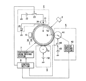
Fig. l schematically shows the construction of
an electrophotographic printing apparatus according to
the first embodiment, centering on major portions. This
electrophotographic printing apparatus is composed of
a photosensitive drum 1, a charging device 2, an
exposure device 3, a development device 4, a transfer
device 5, a cleaning device 6, a photosensitive drum
driving system 7, and a control section 8.
The photosensitive drum 1 is constructed in such
a manner that photoconductive material is applied to the
outer periphery of an aluminum cylinder la to form
206~23~
.
- 16 -
a photoconductive layer lb. The charging device 2,
exposure device 3, transfer device 5, and development
device 4 are arranged in that order around the
photosensitive drum 1 so as to face the outer periphery
of the drum 1.
The charging device 2 is made up of a discharging
unit 21, a high-voltage power supply 22, a switch 23,
a grid 24, and a zener diode 25, which are arranged so
as to form a scorotron type charging device of a known
lo construction.
The exposure device 3, which is composed of, for
example, a laser scanner of a known construction,
partially exposes the photosensitive drum 1 by
projecting on it the laser beam modulated according to
an image to be printed from a laser diode (not shown).
The development device 4 is made up of a
development sleeve 41, a sleeve driving system 42, a
development bias power supply 43, and a switch 44. The
development sleeve 41 retains charged toner (now shown
of the same polarity (the negative polarity, in this
case) as that of the charged potential of the photo-
sensitive drum 1, and carries the toner as it is rotated
by the sleeve driving system 42. The development sleeve
41, which is placed so as to face the photosensitive
drum 1, brings the adhering toner into contact with the
photosensitive drum 1. The development bias power
supply 43 generates a development bias with the same
206223~
.,~
- 17 -
polarity (the negative polarity, in this case) as that
of the charged potential of the photosensitive drum 1
and lower (for example, -200v) than this potential, and
applies it to the development sleeve 41 via the switch
44. The switch 44 provides the ON/OFF control of
application of the development bias to the development
sleeve 41.
The transfer device 5 is composed of a transfer
roller 51 and a high-voltage power supply 52. The
transfer roller 51 is provided so as to press printing
paper (not shown) against the photosensitive drum 1.
The high-voltage power supply 52 supplies to the
transfer roller 51 a high voltage of the opposite
polarity (the positive polarity, in this case) to that
of the charged potential of the photosensitive drum 1.
The cleaning device 6, which has, for example,
a blade brushing against the photosensitive drum 1,
scrapes the toner from the photosensitive drum 1.
The photosensitive drum driving system 7, which is
composed of, for example, a motor and gears, rotates the
photosensitive drum 1.
The control section 8 supervises these starting
timings: the starting timing for the photosensitive drum
driving system 7 to rotate the drum 1; that for the
charging device 2 to charge the photosensitive drum 1;
that for the sleeve driving system 42 to rotate the
development sleeve 41; and that for the development bias
20~22~)
- 18 -
to be supplied to the development sleeve 41.
The operation of the electrophotographic printing
apparatus thus constructed will be described in the
order of control sequence of the control section 8.
First, at the start of printing, the control section 8
permits the photosensitive drum driving system 7 to
rotate the photosensitive drum 1. In response to this
permission, the photosensitive drum driving system 7
starts to rotate the drum 1, which then begins to
revolve (time T1 in Fig. 2).
The control section 8 turns on the switch 23 of the
charging device 2 at the same time that it gives the
photosensitive drum driving system 7 a permission to
rotate the drum 1. In the charging device 2, as soon as
the switch 23 has been turned on, a high voltage
generated by the high-voltage power supply 22 is applied
to the discharging unit 21, which then discharges to
cause the surface of the photosensitive drum 1 to be
charged. At this time, the charged potential of the
drum 1 is kept at a constant breakdown voltage of the
zener diode 25 (at -500v, in this case) by a combination
of the grid 24 and zener diode 25.
When a specified period of time TA has elapsed
(time T2 in Fig. 2) since time Tl (the time required for
a particular point on the drum 1 to move from charging
position A under the charging device 2 to developing
position B under the development device 4), the control
206~2~
,
- 19 -
section 8 instructs the sleeve driving system 42 to
start rotating the development sleeve 41, and at the
same time, turns on the switch 44. Accordingly, the
development device 4 begins to operate at the time that
s a particular point on the drum 1 positioned at charging
position A at the start of charging reaches developing
position B. This allows a development bias produced by
the development bias power supply 43 to be applied to
the development sleeve 41.
After this, the exposure device 3 exposes the
charged photosensitive surface of the drum 1 according
to an image to be printed, thereby forming an
electrostatic latent image on the photosensitive surface
of the drum 1. The development device 4 then develops
the electrostatic image on the photosensitive surface of
the drum 1. This development is performed as follows,
for example. The development sleeve 41 holds charged
toner of the same polarity as that of the charged
potential of the drum 1, and brings the toner into
contact with the drum 1 as it rotates. At this time,
the interaction between the electrostatic image and the
development bias allows toner to selectively adhere to
the photosensitive drum 1. Specifically, toner does not
adhere to the charged portions on the photosensitive
drum 1 because the photosensitive drum 1 is at a higher
potential, whereas it adheres to the exposure-discharged
portions because the drum 1 is at a lower potential. As
~ 20~233
I~
- 20 -
a result, a toner image is formed on the photosensitive
surface of the drum 1.
Then, printing paper (not shown) is inserted
between the photosensitive drum 1 and the transfer
roller 51. Here, a voltage (for example, +500v)
generated by the high-voltage power supply 52 with the
opposite polarity to that of the potential of the toner,
is supplied to the back of the printing paper via the
transfer roller 51. This permits the toner adhering to
the photosensitive surface of the drum 1 to be attracted
electrostatically to the printing paper, with the result
that the toner image on the drum 1 is transferred to the
printing paper. After this, the cleaning device 6
removes the residual toner from the surface of the
photosensitive drum 1.
As noted above, with the present embodiment, at the
start of printing, the development sleeve 41 remains
inoperative until the indefinite-voltage portions on the
photosensitive drum has passed developing position B,
which prevents toner from being supplied onto the
photosensitive drum 1, thereby keeping toner from
adhering to the drum 1 even when the potential of the
drum 1 is lower. This eliminates a waste of toner and
the smearing of the transfer roller 51.
The present invention is not limited to this
embodiment. For example, the transfer device is not
restricted to the roller type, but may be of the brush
2Q6223u
1.~
- 21 -
type or of the noncontacting type such as a discharging
unit. The application of a negative voltage to the
transfer roller is not always necessary and may be
omitted. The body of the photosensitive drum 1 is not
restricted to an aluminum cylinder, but may be a
suitable matter as long as it is formed out of
conductive material. The present invention may be
practiced or modified in still other ways without
departing from the spirit or essential character
thereof.
A second embodiment of the present invention will
be explained, referring to the accompanying drawings.
Fig. 3 is a schematic diagram of an electro-
photographic printing apparatus of the second
embodiment, centering on major portions. The same parts
as those in Fig. 1 are indicated by the same reference
characters, and their detailed explanations will be
omitted.
This electrophotographic printing apparatus is
composed of a photosensitive drum 1, a charging device
2, an exposure device 3, a development device 4, a
cleaning device 6, a photosensitive drum driving system
7, a transfer device 9, a zener diode 10, and a control
section 11.
The transfer device 9 is made up of a transfer
roller 51, a high-voltage power supply 52, a high-
voltage power supply 91, and a switch 92. The transfer
~ 206223i~
roller 51 is provided so as to press printing paper (not
shown) against the photosensitive drum 1. The high-
voltage power supply 52 produces a high voltage of the
opposite polarity (the positive polarity, in this case)
to that of the charged potential of the drum 1. The
high-voltage power supply 91 generates a high voltage of
the same polarity (the negative polarity, in this case)
as that of the charged potential of the drum 1. The
switch 92 provides ON/OFF control of application of a
high voltage to the transfer roller 51 and determines
which high voltage to be applied to this roller 51, a
high voltage generated by the high-voltage power supply
51 or that by the high-voltage power supply 91.
The Zener diode 10 has its anode connected to both
the cathode of the Zener diode 25 and the aluminum
cylinder la of the photosensitive drum 1, and its
cathode connected to the ground.
The control section 11 supervises the starting
timing for the photosensitive drum driving system 7 to
start to rotate the drum 1 and the ON/OFF timings of the
switches 23, 44, and 92.
The operation of the electrophotographic printing
apparatus thus constructed will be described in the
order of control sequence of the control section 11.
Here, it is assumed that on the photosensitive drum 1,
the charging position under the charging device 7, the
developing position under the development device 8, and
~ 20~2~3~3
- 23 -
the transferring position under the transfer device are
point A, point B, and point C, respectively. It is also
assumed that the times required for a particular point
on the photosensitive drum 1 to move from points A to s
and from points B to C are TA and TB, respectively.
First, at the start of printing, the control
section 11 permits the photosensitive drum driving
system 7 to rotate the photosensitive drum l. In
response to this permission, the photosensitive drum
driving system 7 starts to rotate the drum 1, which then
begins to revolve (time Tl in Fig. 4).
The control section 11 also turns on the switch 23
of the charging device 2 at the same time that it gives
the photosensitive drum driving system 7 a permission to
rotate the drum 1. In the charging device 2, as soon as
the switch 23 has been turned on, a high voltage
generated by the high-voltage power supply 22 is applied
to the discharging unit 21, which then discharges to
cause the surface of the photosensitive drum 1 to be
charged. At this time, the charged potential of the
drum 1 is kept at a constant breakdown voltage of the
Zener diode 25 (at -500V, in this case) by a combination
of the grid 24 and zener diode 25.
The cantrol section 11 also causes the switch 92 to
switch to the high-voltage power supply 91 at the same
time that it gives the above-described permission.
When a period of time TA has elapsed (time T2 in
- 2~6223~
- 24 -
Fig. 4) since time Tl, the control section 11 then turns
on the switch 43 of the development device 4. That is,
the switch 43 is turned on at the time when a particular
point on the photosensitive drum 1 positioned at
charging position A at the start of charging reaches
developing position B. This allows a development bias
(-200V, in this case) generated by the high-voltage
power supply 43 to be applied to the development sleeve
41.
In this case, during the interval from when the
rotation of the drum 1 and the charging has been started
until the switch is turned on, that is, before the
indefinite-potential portions on the drum 1 located
between charging position A and developing position B
during the stop of the drum 1 has passed developing
position B, the switch 43 remains in the OFF state,
preventing the development bias from being applied to
the development sleeve 41, with the result that the
potential of the development sleeve 41 is at ov. On
the other hand, because in the photosensitive drum 1,
the aluminum cylinder la is connected to the ground via
the Zener diode 10, the potential of the cylinder la is
at the breakdown voltage (-lOOV, in this case) of the
zener diode 10. Here, it is assumed that the potential
of the aluminum cylinder la is of the same polarity as
that of the development bias and its absolute value is
larger than zero but smaller than the absolute value of
- 20~2233
- 25 -
the development bias voltage. That is, in this
embodiment, if the potential of the aluminum cylinder la
is vb, Vb will be in the range of o > vb > -200.
As described above, while the development sleeve 41
is at a potential of OV, even the lowest potential of
the photosensitive drum 1 is as high as -lOOV, meaning
that the drum 1 is higher in potential than the sleeve
41. As a resuIt of this, there is no forces on the drum
that attract the toner retained by the development
sleeve 41 to the photosensitive drum 1, preventing toner
from adhering to the drum 1 even when the potential of
the photosensitive drum 1 is indefinite.
When a period of time Ts has elapsed (time T3 in
Fig. 4) since time T2, the control section 11 causes the
switch 92 of the transfer device 92 to the high-voltage
power supply 52. Specifically, the switch 92 is
switched to the high-voltage power supply 91 until the
indefinite-potential portions on the drum 1 between
charging position A and developing position B during the
stop of the drum 1 have passed transferring position C,
and from this point on, it is switched to the high-
voltage power supply 52. As a consequence, a negative
high-voltage generated by the high-voltage power supply
91 is applied to the transfer roller 51 until the
indefinite-potential portions have passed transfer
position C, and from this time on, a positive
high-voltage (for example, +500V) produced by the
~ 20622~
- 26 -
high-voltage power supply 52 is applied to the roller
51.
With the transfer roller 51 being applied with a
positive high voltage, a similar mechanism to that in
the first embodiment allows the transfer of toner onto
the printing paper passing between the photosensitive
drum 1 and the transfer drum 51. On the other hand,
with the roller 51 being applied with a negative high
voltage, the toner adhering to the drum 1 is repelled
by the action of the negative high voltage, preventing
the toner from adhering to the transfer roller 51.
Consequently, even when toner physically attaches the
drum 1 at the development device 4, the toner thus
adhering to the drum 1 will not adhere to the transfer
roller 51, preventing the transfer roller 51 from
getting dirty.
As noted above, with the present embodiment,
because the potential of the aluminum cylinder la of the
drum 1 is of the same polarity as that of the
development bias and its absolute value is larger than
zero but smaller (-lOOV) than the absolute value of the
development bias voltage, and at the start of printing,
the application of a development bias to the development
sleeve 41 is suspended until the indefinite-potential
portions on the drum 1 have passed developing position
B, the potential of the drum 1 is always kept higher
than that of the development sleeve 81, during this bias
20,~223~
- 27 -
suspension, in spite of the indefinite potential of the
drum 1, thereby preventing toner from adhering to the
drum 1.
In this embodiment, because the high voltage
applied to the transfer roller 51 is of the same
polarity as that of the charged potential of the drum 1
until the indefinite-potential portions on the drum 1
have passed transferring position C, disabling the
transfer roller 51 from transfer, even a trace of toner
on the drum 1 will never adhere to the transfer roller
51, assuring perfect prevention of the smearing of the
roller 51.
While in the embodiment, the charged potential,
development bias, and transfer voltage are set at the
same value as that of the aluminum cylinder la connected
to the ground, it is desirable that they should be
shifted by the amount of potential applied to the
aluminum cylinder la. Specifically, if the potential of
the aluminum cylinder la is -lOOV as noted earlier, the
charged potential should be -600V, the development bias
-300v, and the transfer voltage +400v.
In the embodiment, the interval during which a high
voltage applied to the transfer roller 51 is of the
opposite polarity to that of the transfer voltage is an
interval from when the charging device 2 begins to
charge until a period of time of TA+TB elapses.
However, by setting the interval to a period of time
206~3~
;
- 28 -
from the start of the charging until the leading edge of
the printing paper reaches transferring position C, it
is also possible to prevent toner from adhering to the
transfer roller 51 even when toner has adhered onto the
charged photosensitive drum 1.
The present invention is not limited to this
embodiment. For instance, the transfer device is not
restricted to the roller type, but may be of the brush
type or of the noncontacting type such as a discharging
unit. The application of a negative voltage to the
transfer roller is not always necessary and may be
omitted. The body of the photosensitive drum 1 is not
restricted to an aluminum cylinder, but may be a
suitable matter as long as it is formed out of
conductive material. The present invention may be
practiced or modified in still other ways without
departing from the spirit or essential character
thereof.
A third embodiment of the present invention will be
explained, referring to the accompanying drawings.
Fig. 4 is a schematic diagram of an
electrophotographic printing apparatus of the third
embodiment, centering on primary portions. The same
parts as those in Fig. 1 are indicated by the same
reference characters, and their detailed explanations
will be omitted.
This electrophotographic printing apparatus is
20~223~
- 29 -
composed of a photosensitive drum 1, a charging device
2, an exposure device 3, a transfer device 5, a cleaning
device 6, a photosensitive drum driving system 7, a
development device 12, and a control section 13.
The development device 12 is made up of a
development sleeve 41, a development bias power supply
43, a reverse bias power supply 121, and a switch 122.
The reverse bias power supply 121 produces a reverse
bias of the opposite polarity (the positive polarity, in
this case) to that of the development bias generated by
the development bias power supply 43. The switch 122
provides ON/OFF control of application of a voltage to
the development sleeve 41 and determines which bias to
be applied to this sleeve 41, the development bias or
the reverse bias.
The control section 13 supervises the starting
timing for the photosensitive drum driving system 7 to
start rotating the drum 1 and the ON/OFF timings of the
switches 23, 53, and 122.
The operation of the electrophotographic printing
apparatus thus constructed will be described in the
order of control sequence of the control section 13.
Here, it is assumed that on the photosensitive drum 1,
the charging position under the charging device 2 and
the developing position under the development device 12
are point A and point B, respectively. It is also
assumed that the time required for a particular point on
20~2~J~
- 30 -
the photosensitive drum 1 to move from point A to point
B is TA.
First, at the start of printing, the control
section 13 permits the photosensitive drum driving
system 7 to rotate the photosensitive drum 1. In
response to this permission, the photosensitive drum
driving system 7 starts to rotate the drum 1, which then
begins to revolve (time Tl in Fig. 6).
The control section 13 also turns on the switch 23
of the charging device 2 at the same time that it gives
the photosensitive drum driving system 7 a permission to
rotate the drum 1. In the charging device 2, as soon as
the switch 23 has been turned on, a high voltage
generated by the high-voltage power supply 22 is applied
to the discharging unit 21, which then discharges to
cause the surface of the photosensitive drum 1 to be
charged. At this time, the charged potential of the
drum 1 is kept at a constant break down voltage of the
Zener diode 25 (at -500v, in this case) by a combination
of the grid 24 and zener diode 25.
At time Tl, the control section 13 also causes the
switch 122 to switch to the reverse bias power supply
121, thereby allowing the reverse bias with the positive
polarity to be applied to the development sleeve 41.
With the development sleeve 41 applied with the reverse
bias, negatively charged toner is electrostatically
attracted to the development sleeve 41.
'"- 206~23D
- 31 -
When a period of time TA has elapsed (time T2 in
Fig. 6) since time Tl, the control section 12 then
causes the selector switch 122 to switch to the develop-
ment bias power supply 43, thereby permitting a negative
development bias to be applied to the development sleeve
41. That is, the development bias is applied to the
development sleeve 41 at the time when a particular
point on the drum 1 positioned at charging position A at
the start of charging reaches developing position B.
From this time on, the printing operation is carried out
according to the known electrophotographic processes as
described in the first embodiment.
With the present embodiment, because, at the start
of printing, a reverse bias is applied to the develop-
ment sleeve 41 until the indefinite-potential portions
on the photosensitive drum 1 have passed developing
position B, toner is electrostatically attracted to the
development sleeve 41 that then traps toner firmly
during the interval of the reverse bias, thereby
preventing toner from adhering to the photosensitive
drum 1.
Consequently, toner will not be wasted and the
transfer roller 51 is kept free from dirt.
The present invention is not limited to the
previous embodiments. For instance, various
requirements for the photosensitive drum 1, including
the charged potential and the polarity, are not
20S~J
....
- 32 -
restricted to those used in the previous embodiments.
The switching timings for applying a voltage to the
development sleeve 41 and to the transfer roller 51 are
not restricted to those explained in the previous
embodiments, but may be any timings as long as they are
after time T2 for the applied-voltage switching timing
with the development sleeve 41, and after time T3 for
the applied-voltage switching timing with the transfer
roller 51. It is desirable that the applied-voltage
switching timing with the transfer roller 51 should be
set taking into account the timing that the printing
paper reaches transferring position C.
The present invention may be practiced or modified
in still other ways without departing from the spirit or
essential character thereof.
A fourth embodiment of the present invention will
be explained, referring to the accompanying drawings.
Fig. 7 is a schematic diagram of an electro-
photographic printing apparatus of the fourth
embodiment, centering on primary portions. The same
parts as those in Figs. 1 and 5 are indicated by the
same reference characters, and their detailed
explanations will be omitted.
This electrophotographic printing apparatus is
composed of a photosensitive drum 1, a charging device
2, an exposure device 3, a cleaning device 6, a
photosensitive drum driving system 7, a development
2~2:~
- 33 -
device 14, a transfer device 15, and a control section
16.
The development device 14 is made up of a
development sleeve 41, a development bias power supply
43, switches 44 and 141. The transfer device 15
contains a transfer roller 51, a high-voltage power
supply 52, and switches 53 and 151.
The switch 141 of the development device 14
provides ON/OFF control of application of a transfer
voltage generated by the high-voltage power supply 52 of
the transfer device 15 to the development sleeve 41.
The switch 151 of the transfer device 15 provides ON/OFF
control of application of a development bias produced by
the development-bias power supply 43 of the development
device 14 to the transfer roller 51.
The control section 16 supervises the starting
timing for the photosensitive drum driving system 7 to
start rotating the drum 1 and the ON/OFF timings of the
switches 23, 44, 53, 141, and 151.
The operation of the electrophotographic printing
apparatus thus constructed will be described in the
order of control sequence of the control section 16.
Here, it is assumed that on the photosensitive drum l,
the transferring position under the transfer device 15
is point C. It is also assumed that the time required
for a particular point on the photosensitive drum l to
move from point B to point C is TB.
20622~
.,
- 34 -
First, at the start of printing, the control
section 16 permits the photosensitive drum driving
system 7 to rotate the photosensitive drum 1. In
response to this permission, the photosensitive drum
driving system 7 starts to rotate the drum 1, which then
begins to revolve (time T1 in Fig. 8).
The control section 16 also turns on the switch 23
of the charging device 2 at the same time that it gives
the photosensitive drum driving system 7 a permission to
rotate the drum 1. In the charging device 2, as soon as
the switch 23 has been turned on, a high voltage
generated by the high-voltage power supply 22 is applied
to the discharging unit 21, which then discharges to
cause the surface of the photosensitive drum 1 to be
charged. At this time, the charged potential of the
drum 1 is kept at a constant breakdown voltage of the
Zener diode 25 (at -500v, in this case) by a combination
of the grid 24 and Zener diode 25.
At time T1, the control section 16 also turns on
the switch 141 of the development device 14 and the
switch 151 of the transfer device 15. When these
devices are not in operation, both the switches 44 and
141 of the development device 14 and the switches 53 and
151 of the transfer device 15 are in the OFF state. The
switch 44 and switch 53 remain in the OFF state even
after the switch 141 and switch 151 have been tuned on.
This permits a positive transfer voltage to be applied
2D~2~0
......
- 35 -
to the development sleeve 41 and a negative development
bias to be applied to the transfer roller 51. With the
development sleeve 41 applied with a ~ositive voltage,
negatively charged toner is electrostatically attracted
to the development sleeve 41. With the transfer roller
51 applied with a negative voltage, even when some toner
exists on the drum 1, there are no electrostatic forces
that attract the toner to the transfer roller 51.
When a period of time TA has elapsed (time T2 in
Fig. 8) since time Tl, the control section 16 turns off
the switch 141 and turns on the switch 44. That is, the
voltage applied to the development sleeve 41 is changed
from the positive transfer voltage to the negative
development bias at the time when a particular point on
the drum 1 positioned at charging position A at the
start of charging reaches developing position B. This
changeover starts a developing operation.
After another time of period TB has elapsed (time
T3 in Fig. 8) since time T2, the control section 16
turns off the switch 151 and turns on the switch 53.
That is, the voltage applied to the transfer roller 51
is changed from the negative development bias to the
positive transfer voltage at the time when a particular
point on the drum 1 positioned at charging position A at
the start of charging reaches transferring position C.
This changeover allows the generation of electrostatic
forces that attract the toner adhering to the
2062~23a
..
- 36 -
photosensitive drum 1 to the transfer roller 51, being
ready for a transferring operation. From this point on,
the printing operation is carried out according to the
known electrophotographic processes as described in the
first embodiment.
As with the third embodiment earlier described,
with the present embodiment, a reverse bias is applied
to the development sleeve 41 until the indefinite-
potential portions on the drum 1 has passed developing
position B, electrostatically attracting toner to the
development sleeve 41. Accordingly, during the interval
of the reverse bias, the development sleeve 41 is
trapping toner effectively, preventing toner from
adhering to the drum 1.
In this embodiment, because the transfer device 15
has the high-voltage power supply 52 that generates a
transfer voltage of the opposite polarity to that of the
charged potential of the drum 1 or that of the develop-
ment bias, this power supply 52 is also used as a power
supply to apply a reverse bias to the development sleeve
41, thereby achieving the lower production cost and the
more compact, less-power consuming design of the
apparatus. If the transfer voltage is not suitable for
the development sleeve 41 or the development bias is not
desirable for the transfer roller 51 (generally, the
transfer voltage is higher than a voltage to be applied
to the development sleeve 41), adjustment is necessary
206~230
- 37 -
by, for example, adding a suitable resistor.
Because a development bias generated by the
development bias power supply 43 continues to be applied
to the transfer roller 51 until the indefinite-potential
portions on the drum 1 have passed transferring position
C, the toner adhering to the drum 1 can be prevented
effectively and economically from adhering to the
transfer roller 51, without providing an additional
power supply.
The present invention is not limited to the
previous embodiments. For instance, various
requirements for the photosensitive drum 1, including
the charged potential and the polarity, are not
restricted to those used in the previous embodiments.
The switching timings for applying a voltage to the
selection sleeve 41 and to the transfer roller 51 are
not restricted to those explained in the previous
embodiments, but may be any timings as long as they are
after time T2 for the applied-voltage switching timing
with the development sleeve 41, and after time T3 for
the applied-voltage switching timing with the transfer
roller 51. It is desirable that the applied-voltage
switching timing with the transfer roller 51 should be
set taking into account the timing that the printing
paper reaches transferring position C.
Although in the above embodiment, adhesion of toner
to the transfer roller 51 is prevented by applying
2û~2~3~
- 38 -
a development bias to the transfer roller 51, the
application of development bias may be omitted provided
that toner adhesion to the drum 1 at the development
device 14 is sufficiently prevented or a noncontacting
transfer unit such as a corona discharging unit is used.
While in the embodiment, the transfer roller 51 is used,
a brush, a belt, or a noncontacting type unit such as
a corona discharging unit may be use.
The present invention may be practiced or modified
in still other ways without departing from the spirit or
essential character thereof.
A fifth embodiment of the present invention will be
explained, referring to the accompanying drawings.
Figs. 9 and 10 are schematic diagrams of an
electrophotographic printing apparatus of the fifth
embodiment, centering on primary portions. Fig. 9 is
the side view and Fig. 10 is the perspective view. The
same parts as those in Fig. 1 are indicated by the same
reference characters, and their detailed explanations
will be omitted.
This electrophotographic printing apparatus is
composed of a photosensitive drum 1, a charging device
2, a photosensitive drum driving system 7, a development
device 17, a solenoid 18, a body plate 19, and a control
section 20. Although it also contains an exposure
device, a transfer device, and a cleaning device like
the first embodiment, they are omitted in the figure.
20~22~0
- 39 -
The development device 17 iS made up of a
development sleeve 41, a hopper 171, a rotation
instructing pin 172, a hook 173, and a spring 174. The
hopper 171 stores toner. The development sleeve 41, a
5 large proportion of which is located inside the hopper
171, is in contact with the toner stored in the hopper
171. The sleeve 41, a portion of which projects outside
the hopper 171, carries the stored toner from the hopper
171 as it rotates. The projecting portion outside the
hopper 171 of the sleeve 41 is very close to the
photosensitive drum 1. The rotation instructing pin 172
is provided above the development sleeve 41 with its
axis in parallel with that of the development sleeve 41.
This pin 172 iS installed in a body (not shown) so as to
rotate freely. The hook 173 is installed on the side
(the back end) of the hopper 171 from which the
development sleeve is not projecting (hereinafter,
referred to as the back end). One end of the spring 174
is hooked to the hook 173. The other end of the spring
174 - iS hooked to the body plate 19 secured to the not-
shown body. The spring 174 pUlls up the hook 173, that
is, the back end of the hopper 171.
The solenoid 18 is fixed to the not-shown body so
that a moving section 18a may be movable vertically.
The solenoid 18 is also positioned so that the moving
section 18a in the lower position may press down the
back end of the hopper 171.
~ 20~223~
- 40 -
The control section 20 supervises the starting
timing for the photosensitive drum driving system 7 to
rotate the drum 1, that for the charging device 2 to
charge the photosensitive drum 1, and the up-and-down
motion timings of the solenoid 18.
The operation of the electrophotographic printing
apparatus thus constructed will be described in the
order of control sequence of the control section 20.
When the apparatus is not in operation, the moving
section 18a of the solenoid 18 is in the upper position.
In this state, the hopper 171 is being pulled up at its
back end, tilting as shown by the broken lines in
Fig. 9. Supported by the hopper 171, the development
sleeve 41 moves as shown by the broken lines in Fig. 9,
as the hopper 171 tilts. As a result of this motion,
the development sleeve 41 is kept apart from the
photosensitive drum 1.
In this state, to start a printing operation, the
control section 20 first permits the photosensitive drum
driving system 7 to rotate the photosensitive drum 1.
In response to this permission, the photosensitive drum
driving system 7 starts to rotate the drum 1, which then
begins to revolve (time Tl in Fig. 11).
The control section 20 also turns on the switch 23
of the charging device 2 at the same time that it gives
the photosensitive drum driving system 7 a permission to
rotate the drum 1. In the charging device 2, as soon as
2062~30
- 41 -
the switch 23 has been turned on, a high voltage
generated by the high-voltage power supply 22 is applied
to the discharging unit 21, which then discharges to
cause the surface of the photosensitive drum 1 to be
charged. At this time, the charged potential of the
drum 1 is kept at a constant breakdown voltage of the
Zener diode 25 (at -500v, in this case) by a combination
of the grid 24 and Zener diode 25.
When a specified period of time TA (the time
required for a particular point on the drum 1 to move
from charging position A under the charging device 2 to
developing position B under the development device 4)
has elapsed (time T2 in Fig. 11) since time Tl, the
control section 20 energizes the solenoid 18 to move
down the moving section 18a. That is, the moving
section 18a of the solenoid 18 is moved downward at the
time when a particular point on the drum 1 positioned at
charging position A at the start of charging reaches
developing position B. ThiS downward movement causes
the development sleeve 41 to move nearer to the
photosensitive drum 1.
From this point on, the printing operation is
carried out according to the known electrophotographic
processes as described in the first embodiment.
As described above, with the present embodiment,
because at the start of printing, the development
sleeve 41 is kept apart from the drum 1 until the
20S2230
- 42 -
indefinite-potential portions on the drum 1 have passed
developing position B, toner will not be supplied onto
the drum 1 during this interval, thus preventing toner
from adhering to the drum 1 even when the potential of
the drum 1 is lower. Accordingly, a waste of toner can
be avoided and the transfer roller be kept free from
dirt.
The present invention is not restricted to the
above embodiment. For instance, the mechanism for
separating the development sleeve 41 from the drum 1 is
not limited to than in the above-described embodiment.
The present invention may be practiced or modified in
still other ways without departing from the spirit or
essential character thereof.