Note: Descriptions are shown in the official language in which they were submitted.
S P E C I F I C A T I O N 0 6 ~4
Title of the Invention
A thin film of oxide superconductor possessing locally different crystal
orientations and processes for preparing the same
Back~round of the Invention
Field of the Invention
The present inventioll relates to a thin film of oxide superconductor
10 possessing locally different crystal orientations and more particularly to a
process for producing a thin film of oxide superconductor having a-axis
(or b-axis) oriented tllin film portions and c-axis oriented thin film
portions on a common substrate and processes for preparing the same.
Description of the related arts
Oxide superconductors are expected to be used in a variety
applications due to their lli~her critical temperatures than conventional
metal superconductors. In fact. Y-Ba-Cu-O oxide superconductor possess
the critical temperature above 80 K and Bi-Sr-Ca-Cu-O and Tl-Ba-Ca-
Cu-O oxide superconductors possess the critical temperature above ]00
K. However, the oxide superconductors possess crystal anisotropy in
their superconductill~ properties. In fact, the highest critical current
density is observed in a direction ~-hich is perpendicular to c-axis of their
crystal. From this fact, the direction of crystal orientation must be
2 5 considered in actual utilization of oxide superconductors.
In the oxide superconductors to which the present invention is
applicable, a-axis, b-axis and c-axis of their crystals are deterrnined and
known. It is also knowlt that electric current flows in a plane defined by
~'
2062294
the a-axis and the b-axis. In the specification, only a-axis oriented thin
film is referred because difference between an a-axis oriented thin film
and a b-axis oriented thin film is not import from the view point of
supereondueting eurrent flow. Orientation of these axes is usually
5 defined by the direction of crystal axis with respect to a surfaee of the
substrate. For example, "c-axis oriented thin film" means a thin film
whose e-axis is perpendicular to the surface of substrate.
When the oxide superconductors are used in superconduetor
eleetronics for producing superconducting devices or integrated
10 superconducting circuits, it is indispensable to prepare a thin film of the
oxide supereonductors. However, the problem of crystal anisotropy
beeome mueh critical in the thin films of oxide superconductors.
In addition to this, in order to realize high-performanee
supereondueting devices or integrated supercondueting circuits of high
15 density, it is requested to prepare, on a common surface of substrate, two
kinds of superconducting wiring lines: one in which electric current
flows in parallel with a surface of substrate and another in which electrie
current flows perpendicular to the surfaee of substrate. For example, in
supereondueting electrodes, current flows usually in parallel with the
20 surfaee of substrate while in interlayer superconducting wiring lines
eonneeting different layers stratified on the substrate, current must flow
perpendicular to the surface of substrate. Therefor, when oxide
supereonductor is used in high-performance superconducting devices or
integrated superconducting circuits of high density, it is requested to
25 deposit, on a common surface of a substrate, both of c-axis orientated
thin film of oxide superconductor in which the critical current density
along the direction whicll is in parallel with the surfaee of substrate is
higher than the other directions and of a-axis (or b-axis) orientated thin
2062294
film of oxide superconductor in which the critical current density along
the direction which is pelpendicular to the surface of substrate is higher
than the direction of c-axis.
Crystal orientation of the thin film of oxide superconductor can be
5 controlled by selecting film-forming temperature which is determined
usually by substrate temperature. In fact, the a-axis oriented thin film
can be realized at a substrate temperature which is lower by about 50 to
100 C than a substrate temperature which is preferable to prepare the c-
axis oriented thin film. From this fact, in a known process for preparing
10 a thin film having a-axis oriented thin film portions and c-axis oriented
thin film portions in a common substrate, one of the thin film portions is
deposited firstly on a surface of the common substrate, then selected area
of the firstly deposited thill film portions are removed by etching
technique to produce patterned first thin film portions and after that,
15 another thin film portions ale deposited on the selected area.
This known techni4ue~ however, is not effective in actual
production because it is necessary to effect two deposition steps of two
different thin films under different conditions. Still more, the dimension
of superconducting wiring lines obtained is limited due to tolerance or
2 0 precision of etching operation, so that a cross section of a
superconducting wiring line obtained becomes unnecessarily large,
resulting in that it is diffic~llt to increase the density of superconducting
circuits. There is also such danger that the thin film of oxide
superconductor obtained is contaminated at etched margins or non-
2 5 superconductor deposit on the etched margins. Still more, when etchingoperation is not effected satisfactorily, for example, when a firstly
deposited c-axis oriented thin ~llm is not removed completely but is left,
next thin film deposited on the firstly deposited c-axis oriented thin film
~-.
- 2062294
will not become an a-axis oriented thin film but becomes a c-axis oriented
thin film. Even if the firstly deposited thin film can be removed
completely, the resulting surface is often roughened due to delicate
operational conditions of etching. In such case also, it is difficult to
S realize a well-ordered a-axis oriented thin film of high quality.
The known process has another problems. Namely, when a c-axis
oriented thin film is deposited firstly and then an a-axis oriented thin film
is deposited secondly, even if the etching operation is effected ideally,
oxygen atoms escape out of the margin of the c-axis oriented thin film
10 which are exposed by etching operation, so that the stoichiometry of the
thin film is spoiled at the margins of the c-axis oriented thin film,
resulting in deterioration of superconducting properties at the margins.
In this case, after deposition of an a-axis oriented thin film is effected. it
is impossible to re-supply oxygen atoms to the marginal area of the c-axis
15 oriented thin film by conventional oxygen supply technique such as heat-
treatment, because the marginal area is filled or closed with the a-axis
oriented thin film and hence oxygen can't enter the c-axis oriented thin
film due to such a fact that oxygen can enter only through the plane
defined by a-axis and b-axis. Therefore, a superconducting device
2 0 obtained sometimes does not work.
Still more, in the knowll process, it is very difficult to realize a
perfect or satisfactory interface between a c-axis oriented thin film
deposited firstly and an a-axis oriented thin film deposited secondly,
resulting in that the capacity of electric current at the interface is limited.
2 5 And, a weak junction caused by the contamination at the etching operation
is often produced at the interface between the a-axis oriented thin film
and the c-axis oriented thin film, resulting in that the obtained
. r
- 20622q4
superconductin~ device ~hows non~ lear property due to a tunnel
current.
An object of the present invention is to solve the problems of the
known process and to provide an improved thin film of oxide
5 superconductor possessing locally different crystal orientations and a process for preparing the superconductor.
SUMMARY OF THE INVENTION
In one aspect, the present invention provides a superconductor
comprising a first portion consisting of c-axis oriented thin film of oxide
superconductor and a second portion consisting of a-axis oriented thin film
of oxide superconductor, each portion being deposited on a different buffer
layer portion deposited on a substrate, and said differently oriented portions
15 of thin film of oxide superconductor being juxtaposed on said different
buffer layer portions.
A second aspect of the invention provides a process for preparing a
superconductor comprising a first portion consisting of c-axis oriented thin
film of oxide superconductor and a second portion consisting of a-axis
2 0 oriented thin film of oxide superconductor, characterized by the steps of
depositing a first buffer layer on a substrate, removing a selected portion of
said first buffer layer to expose a surface of said substrate, depositing a second
buffer layer on the exposed surface, and depositing a thin film of oxide
superconductor on the first buffer layer remaining on the second buffer
2 5 layer, so that differently oriented portions of said thin film of oxide
superconductor are deposited and juxtaposed on different buffer layer
portions.
B
2062294
Description of the Preferred Embodiments
First Embodiment
In the first embodilllellt in which the thin under-layer is made of
buffer layers, the thin film of oxide superconductor according to the
present invention consists of first portions which are deposited on first
b~ tr 1~ _ ~ ~ ~ ~ ~ ~ re
,, ~
- - 2062294
that a thin film of oxide superconductor whose c-axis is oriented along a
direction which is perpendicular to the substrate is easily grown and of
second portions which are deposited on second buffer layer portions
made of a material having such a crystal structure that a thin film of
S oxide superconductor whose c-axis is oriented along a direction which is
in parallel to the substrate is easily grown.
The thin film of oxide superconductor according to the first
embodiment is prepared by the steps of depositing a first buffer layer on
said substrate, removing selected portions of said first buffer layer to
1 0 expose a surface of said substrate, depositing a second buffer layer on the
exposed surface, and thell depositing a thin film of oxide superconductor
on the first buffer layer.portions remained and on the second buffer
layer.
The obtained thin film of oxide superconductor consists of c-axis
15 oriented portions in which c-axis of crystal is oriented along a direction
which is perpendicular to the substrate and a-axis oriented portions in
which c-axis of crystal is oriented along a direction which is in parallel
with the substrate, so that the directions of electric current can be selected
according to respective uses of the thin film of oxide superconductor of
20 which superconducting wiring lines, superconducting electrodes or the
like are fabricated, resulting in that high-performance superconducting
devices or integrated supercondllcting circuits can be realized.
The process of the first embodiment is applicable to any known
oxide superconductor and is advantageously applicable to Y-Ba-Cu-O
2 5 oxide superconductor, Bi-Sr-Ca-Cu-O oxide superconductor and Tl-Ba-
Ca-Cu-O oxide supercollductor which have the most attractive properties
including the critical temperature.
-
2n622q4
The buffer layers to be deposited on the substrate are selected
preferably in such a mamler that the portion of the buffer layer on which
c-axis oriented thin film of oxide superconductor is to be deposited is
made of LaA103, PrGaO3 or the like, while the portion of the buffer
layer on which a-axis oriented thin film of oxide superconductor is to be
deposited is preferably made of A1203, MgO or the like. This is because
the crystal lattice of LaA103, PrGaO3 or the like well-matches or is
compatible with that of a-axis or b-axis oriented thin film of oxide
superconductor to be deposited thereon and a c-axis oriented thin film of
oxide superconductor can be grown easily on these buffer layers.
The thin film of oxide superconductor is preferably prepared at a
substrate temperature in which c-axis oriented thin film of oxide
superconductor grows. This is because a desired crystalline thin film can
be obtained at higher substrate temperatures and growth of the c-axis
oriented thin film of oxide superconductor requires a higher substrate
temperature than that for the a-axis oriented thin film of oxide
superconductor. In the process according to the present invention, both
of c-axis and a-axis oriented thin film portions of oxide superconductor
grow spontaneously at the same substrate temperature.
2 0 Second Embodiment
In the second embodiment in which the under-layer is made of a
very thin film of oxide superconductor, the thin film of oxide
superconductor according to the present invention consists of of first
portions whose c-axis of crystal is in parallel with a surface of a substrate
2 5 at first selected area of the surface and second portions whose c-axis of
crystal is perpendicular to the surface at second selected area of the
surface, the first portions being deposited on a very thin under-film layer
of oxide superconductor whose c-axis of crystal is in parallel with the
206229~
surface and which is deposited previously on the substrate while the
second portions being deposited directly on the substrate.
The thin film of oxide superconductor of the second embodiment
can be prepared by the steps of protecting or covering the second selected
S area of the surface with a sublimatable metal having a higher sublimation
temperature than a film forming temperature of the the second portions,
depositing a very thin under-film layer of oxide superconductor whose c-
axis of crystal is in parallel with the surface whole over the first and
second area, elevating a substrate temperature to sublimate the metal in
10 order to remove parts of the ullder-film layer together with the metal so
as to expose the second selected area of the substrate and then deposing a
thin film of oxide superconductor on the under-film layer at the first
area and on the second area exposed under such a condition that is
suitable to effect growtll of a c-axis oriented thin film of oxide
1 5 superconductor.
An essence of the second embodiment resides in that a very thin
under-Iayer of oxide supelcollductor whose c-axis of crystal is in parallel
with the surface is deposited firstly on the first selected area and then
deposition of a thin film of oxide superconductor is carried out under
2 0 such condition that c-axis of the thin film of oxide superconductor grows
along a direction whicll is perpendicular to the surface.
The very thin under-lclyel of oxide superconductor is can be made
of the same material as the thin film which is deposited finally.
It is confirmed tllat the a-axis oriented thin film of oxide
25 superconductor grows on the very thin under-layer of a-axis oriented
oxide superconductor which is deposited previously even under a
condition where a-axis of the thin film of oxide superconductor usually
grows along a direction which is in parallel with the surface. Therefore,
2062294
the thin film obtained possesses both of first portions whose c-axis of
crystal is in parallel with a surfdce of the substrate at ~lrst selected area ofthe surface and of second portions whose c-axis of crystal is
perpendicular to the surface at second selected area of the surface.
5 Therefore, the directions of electric current can be selected according to
respective uses of the thin film of oxide superconductor of which
superconducting wiring lines, superconducting electrodes or the like are
fabricated, so that high-performance superconducting devices or
integrated supercollductillg circ-lits can be realized.
The very thin under-layer of oxide superconductor has preferably a
thickness of less than about 50 nlll corresponding to a thickness where an
a-axis oriented thin film of oxide superconductor changes from cluster
growth to a film growth.
The sublimatable metal can be Mo. In oxygen containing
15 atmosphere at about 790 C. Mo changes to MoO3 which sublimates. Mo
gives no or little bad influellce to the thin film of oxide superconductor.
The substrate is preferably MgO, PrGaO3 or the like.
The process according to the second embodiment is also applicable
to any known oxide superconductor and is advantageously applicable to
20 Y-Ba-Cu-O oxide superconductor, Bi-Sr-Ca-Cu-O oxide superconductor
and Tl-Ba-Ca-Cu-O oxide supelconductor which have the most attractive
properties including the cliticcll temperature.
In the processes according to the present invention, a thin film of
oxide superconductor possessing locally different crystal orientations can
2 5 be realized easily by a single step of deposition and the superconducting
properties of the superconducting oxide thin film are not spoiled because
the thin film is not subjected to undesirable operations.
,
- ~2062294
The thin film of oxide superconductor prepared by the processes
according to the present invention possesses locally different crystal
orientations whose interfaces have good condition and hence shows
improved superconducting properties which are requested for realizing
5superconducting devices or integrated superconducting circuits.
Now, the present invention will be described with reference to
Examples but the scope of the invention should not be limited thereto.
Brief Description of the Drawings
10Fig. 1 illustrates successive steps of the first embodiment according
to the present inventioll.
Fig. 2 illustrates successive steps of the second embodiment
according to the present invelltion.
15Description of the Preferred Embodiments
Example 1
A thin film of YlBa2Cu3O7 x having a-axis oriented portions a~d
c-axis oriented portions on a common surface of MgO substrate by a
process according to the first embodiment of the present invention.
20The process accordillg to the present invention will be described
with referring to an attached drawing.
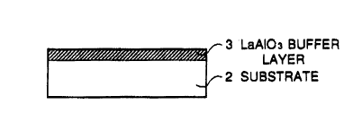
At first, a buffer layer (3) of LaAlO3 having a thickness of about
200 nm is deposited firstly on a substrate (2) as is shown in Fig. lA by
sputtering. The substrate (2) is preferably of insulator such as MgO
25(100), SrTiO3, CdNdAI04 or the like or of semiconductor such as
silicon. The buffer layer (3) can be also of PrGaO3. A photo-resist layer
(50) is formed on a surface of the buffer layer (3) as is shown in Fig. lB.
When LaAlO3 is selected as the buffer layer (3), selected portion of the
2n62294
buffer layer (3) at whicll an a-axis oriented thin film of oxide
superconductor is to be deposited is removed by patterning process.
Fig. lC shows a patterned photo-resist layer having remained photo-
resist area (51, 52). Then, the patterned photo-resist layer is subjected to
5 ion milling or reactive ion etching operation to remove non-protected
portion (5) of the buffer layer (3) until a surface of the substrate (2) is
exposed between adjacent two buffer layer portions (31, 32) protected by
the photo-resist area (51, 52). Then, another buffer layer (4) of A12O3 is
deposited up to the same thickness as the adjacent buffer layer portions
1 0 (31, 32) as is shown Fig. I D. The buffer layer A12O3 may be replaced
by a buffer layer of MgO. Then, layers (41, 42) of A12O3 deposited on
the photo-resist area (51, 52) are removed by lift-off technique of the
latter so that the buffer layer portions (31, 32) are exposed as is shown in
Fig. lE. In this case, if necessary, side walls can be eliminated by side-
15 etching technique. Removal of portions of the buffer layer (3) can beeffected by known other techniques. For example, a hole of non-
protected portion (5) of the buffer layer (3) is filled with suitable
material and then whole surface of deposited layers are subjected to etch-
back operation. After the buffer layer portions (31, 32) are exposed as is
20 shown in Fig. lE, whole surface of exposed buffer layer portions (31,
32) of LaAlO3 and of buffer layer (4) of Al2O3 is subjected to cleaning
operation which can be carried out by irradiating the whole surface with
slant ion shower (in which an axis of ion shower makes an acute angle
with respect to the surface). Finally, as is shown in Fig. lF, a thin film
25 of oxide superconductor is deposited on the buffer !ayers (31, 32) of
LaAlO3 and on a buffer layer (4) of A12O3 by known technique such as
off-axis sputtering, reaction-evaporation, molecular beam epitaxy (MBE)
or chemical vapour deposition (CVD), so that c-axis oriented thin film
1 1
YJ
,~ .~,
2062294
portions (11, 12) are growll on the buffer layer portions (31, 32) of
LaAl03 while an a-axis oriented thin film portion (10) is grown on the
buffer layer (4) of Al203. The off-axis sputtering is carried out for
example under following operational conditions:
Sputtering gas Ar : 90 %
2 : 10%
Pressure : 10 Pa
Substrate temperature : 650 to 700 C
1 0 Example 2
A thin film of YIBa2Cu307 x having a-axis oriented portions and
c-axis oriented portions on a common surface of PrGaO3 substrate as is
shown in Fig. 2A by a process according to the second embodiment of the
present invention.
At first, a layer (60) of Mo having a thickness of about 100 nm is
deposited firstly on a substrate (2) as is shown in Fig. 2B by electron
beam evaporation or CVD. The substrate (2) of PrGaO3 can be replaced
by insulator which is preferably MgO (100), SrTiO3 (100), CdNdA104
(001) or the like or by semiconductor such as silicon having a buffer
2 0 layer. Then, selected portion (6) of the Mo layer (60) is subjected to
argon ion milling or reactive ion etching until a surface of the substrate
(2) is exposed while a pattem (61~ 62) of the Mo layer is left (Fig. 2C).
Then, a very thin a-axis oriented film (lOO, 101, 102) of oxide
superconductor is deposited (Fig. 2D). This a-axis oriented thin film of
25 oxide superconductor can be prepared by off-axis sputtering under
following operational conditiolls:
Sputtering gas A r : 90 %
2 : 10%
12
, .
2n622q~
Pressure : 10 Pa
Substrate temperature : 600to 650 C
Then, the substrate (2) is heated to a temperature between 800 and
850 C at which the remaining Mo layers (61, 62) are sublimated, so that
5 a-axis oriented film portions (101, 102) of oxide superconductor
deposited on the patterned Mo layer (61, 62) are also removed and a
surface of the substrate (2) is exposed except a portion (100) of the a-axis
oriented film of oxide superconductor left as is shown in Fig. 2E. After
then, the substrate (2) is heated to a temperature between 700 and 750 C
10 which is a suitable to grow a c-axis oriented thin film of oxide
superconductor. Then, a thin film of oxide superconductor is deposited
(Fig. 2F). This thin film of oxide superconductor can be prepared by
off-axis sputtering under following operational conditions:
Sputtering gas Ar : 90 %
1 5 O, : 10 ~c
Pressure : 10 Pa
Substrate temperature : 700to 750 C
The resulting thin film of oxide superconductor possesses a-axis oriented
thin film portion (10) grown on the portion (100) of the a-axis oriented
20 film of oxide superconductor left and c-axis oriented thin film portions
(11, 12) grown on the exposed portion of the substrate (2).
~,