Note: Descriptions are shown in the official language in which they were submitted.
CA 02062414 1998-0~-06
-
A CIRCUIT FOR INTERCONNECTING
INTEGRATED SEMICONDUCTOR CIRCUITS
The invention relates to a circuit (hereinafter referred to as an
interconnection circuit) for interconnecting two integrated semiconductor circuits
for transferring a logic signal of a given level from one of said integrated circuits
to the other, said interconnection circuit being provided in the signal path
5 therebetween with a terminal resistor for adjusting impedances.
Electronic devices for data processing and data communication are
generally designed to permit fast data transmission between semiconductor
circuits in a device. For example, in those portions where especially fast
operations are needed, bipolar semiconductor circuits including emitter-coupled
10 logic (ECL) are used, while in other portions CMOS semiconductor circuits are used.
In cases when coexisting semiconductor circuits have different
characteristics as mentioned above, it may be that the operating levels of the
semiconductor circuits are not the same. Accordingly, then, an output of a
15 semiconductor circuit may not be directly coupled to other semiconductor
circuits.
Conventionally, when the output level of a first semiconductor
circuit is different from the input level of a second semiconductor circuit to be
connected with the first circuit, a level converter is provided between them so
20 that the output level of the first circuit is adjusted or matched to that of the
second circuits, as shown in Figure 1.
A typical converter 5 shown in Figure 1 is installed between an
output buffer 2 for a CMOS circuit 1 consisting of CMOS semiconductors and
an input buffer 4 for a bipolar circuit 3. Such inverter is designed to convert the
25 level of the logic signal SO of the CMOS circuit 1 to the level of the input Sl of
the bipolar circuit 3.
The level converter 5 includes a CMOS circuit coupled with a
bipolar circuit, and may convert the logic level of the CMOS circuit in the range
of 0 - 5 volts to the logic level of the ECL (bipolar logic) in the range of -0.8 to
CA 02062414 1998-0~-06
-1.7 volts.
However, such prior art has the following disadvantages.
Firstly, it requires an independent converter 5, which implies that
additional components are required in manufacturing an electronic device,
5 thereby not only harming the cost efficiency of device manufacture but also
using up extra space within the substrate for the converter. Furthermore, the
converter requires extra electric power.
Another serious problem pertinent to such converter 5 is that when
the distance between the CMOS circuit 1 and the converter 5 is long, floating
10 capacitance formed in the circuit board bearing them becomes so great that the
operational speed of the CMOS circuit 1 will be lowered for a large output load.This will impede fast signal transfer between the circuits.
The invention is aimed to overcome the disadvantages as
mentioned above, that is, to provide an interconnection circuit for realizing fast
15 signal transfer between semiconductor circuits.
In order to carry out the object of the invention, there is provided
in a first example an interconnection circuit for interconnecting two integratedsemiconductor circuits for transferring a logic signal of a given level from oneof said integrated circuits to the other through a signal path therebetween. The20 interconnection circuit is provided with a terminal resistor in the signal path for
adjusting impedances.
In a first form, the interconnection circuit has a first circuit
connectable to an output point of one of said semiconductor circuits, the first
circuit comprising an inverter circuit, a first p-channel MOS transistor, and a
25 second p-channel MOS transistor. The input of the inverter circuit is connected
to the output point. The first p-channel MOS transistor has its gate connected
to the output of the inverter circuit. The second p-channel MOS transistor has
its drain coupled to the source of the first p-channel MOS transistor, and its gate
coupled to the output point. The source of the first p-channel MOS transistor
30 and the drain of the second p-channel MOS transistor are connected at a
common node. The drain of the first p-channel MOS transistor is connected to
CA 02062414 1998-0~-06
-
a voltage source. The source of the second p-channel MOS transistor is
connected to ground. The interconnection circuit also has a signal path
connected to the common node and, through a first terminal resistor, to the
voltage source. The interconnection circuit further has a second circuit
5 connectable to the input of the other of the semiconductor circuits and to thesignal path. The second circuit comprises a circuit for discriminating the levels
of a signal on the signal path by a threshold value which is approximately
intermediate the maximum and the minimum of the levels of the signal on the
signal path. The interconnection circuit may additionally comprise a reference
10 signal generator circuit connected to the voltage source through a second
terminal resistor and also connected to the second circuit for providing an
external threshold value for the second circuit.
In this arrangement, the logic level (H) of the output circuit is
maintained on one hand at substantially the same level as the power source
15 voltage, and on the other hand the logic low (L) is maintained at a level equal
to the power source voltage minus the threshold voltage of the p-channel MOS
transistor, multiplied by the ratio of the resistance of the terminal resistor to the
sum of the terminal resistance and the ON-state resistance of the second p-
channel MOS transistor. Accordingly, the amplitude of the logic level is made
20 smaller, so that fast signal transfer may be attained. In addition, since a
reference signal generator circuit is provided for generating a threshold level
which is little affected by external influences, discrimination of the logic levels
may be carried out under a stable condition.
In a second form of the interconnection circuit, the first circuit may
25 additionally have third and fourth p-channel MOS transistors. The third p-
channel MOS transistor has its gate connected to the output of the inverter
circuit. The fourth p-channel MOS transistor has its drain coupled to the sourceof the third p-channel MOS transistor, and has its gate coupled to the output
point. In this arrangement, the source of the first p-channel MOS transistor and30 the drain of the second p-channel MOS transistor are connected at a first
common node, and the source of the third p-channel MOS transistor and the
CA 02062414 1998-0~-06
drain of the fourth p-channel MOS transistor are connected at a second
common node. The drain of each of the first and third p-channel MOS
transistors are connected to a voltage source, and the source of each of the
second and fourth p-channel MOS transistors are connected to ground. A first
5 signal path is connected to the first common node and, through a first terminal
resistor, to the voltage source. A second signal path is connected to the secondcommon node and, through a second terminal resistor, to the voltage source.
The second form of the interconnection circuit has a second circuit that is
connectable to the input of the other of the semiconductor circuits and to the
10 first and second signal paths. The second circuit includes a comparator for
discriminating the levels of an output of the first circuit by comparing the levels
of the first and second signal paths.
In the foregoing interconnection circuits, influence of external noise
is minimized, since the input logic is provided in two mutually-inverted levels
15 from the output circuit, and hence the input circuit may discern the output logic
from the difference between the output levels.
In the first and second forms of the interconnection circuits, the
one integrated semiconductor circuit is preferably a CMOS semiconductor
circuit, while the other integrated semiconductor circuit is preferably a bipolar
20 semiconductor circuit. In this case it is easy to construct a proper input circuit
suitable for logic discrimination even when the threshold is close to the power
source voltage.
The reference signal generator circuit may include paired first and
second p-channel MOS transistors, and also a third p-channel MOS transistor
25 and a fourth p-channel MOS transistor. The gates of the first and second p-
channel MOS transistors are connected to ground. The drain of the second p-
channel MOS transistor is connected to the source of the first p-channel MOS
transistor at a second common node. The drain of the first p-channel MOS
transistor is connected to the voltage source. The source of the second p-
30 channel MOS transistor is connected to ground. The third p-channel MOS
transistor has its gate connected to ground and has its drain connected to the
CA 02062414 1998-0~-06
voltage source. The fourth p-channel MOS transistor has its gate connected to
the second common node, has its source connected to ground, and has its drain
connected to the source of the third p-channel MOS transistor at a third
common node. The voltage on the third common node provides the external
5 threshold value for the second circuit.
Since this reference signal generator circuit may be constructed
solely by p-channel MOS transistors, it is easy to include one in an integrated
semiconductor circuit, thereby minimizing the size of the circuit.
In a third form, the interconnection circuit has a first circuit
10 connectable to an output point of one of said semiconductor circuits, the first
circuit comprising an inverter circuit, a first n-channel MOS transistor, and a
second n-channel MOS transistor. The input of the inverter circuit is connected
to the output point. The first n-channel MOS transistor has its gate connected
to the output of the inverter circuit. The second n-channel MOS transistor has
15 its drain coupled to the source of the first n-channel MOS transistor, and its gate
coupled to the output point. The drain of the first n-channel MOS transistor andthe source of the second n-channel MOS transistor are connected at a common
node. The source of the first n-channel MOS transistor is connected to a
voltage source. The drain of the second n-channel MOS transistor is connected
20 to ground. The interconnection circuit also has a signal path connected to the
common node and, through a first terminal resistor, to ground. The
interconnection circuit further has a second circuit connectable to the input ofthe other of the semiconductor circuits and to the signal path. The second
circuit comprises a circuit for discriminating the levels of a signal on the signal
25 path by a threshold value which is approximately intermediate the maximum andthe minimum of the levels of the signal on the signal path. The interconnection
circuit may additionally comprise a reference signal generator circuit connectedto the voltage source through a second terminal resistor and also connected to
the second circuit for providing an external threshold value for the second
30 circuit.
CA 02062414 1998-0~-06
In a fourth form of the interconnection circuit, the first circuit may
additionally have third and fourth n-channel MOS transistors. The third n-
channel MOS transistor has its gate connected to the output of the inverter
circuit. The fourth n-channel MOS transistor has its source coupled to the drainof the third n-channel MOS transistor, and has its gate coupled to the output
point. In this arrangement, the drain of the first n-channel MOS transistor and
the source of the second n-channel MOS transistor are connected at a first
common node, and the drain of the third n-channel MOS transistor and the
source of the fourth n-channel MOS transistor are connected at a second
common node. The source of each of the first and third n-channel MOS
transistors are connected to a voltage source, and the drain of each of the
second and fourth n-channel MOS transistors are connected to ground. A first
signal path is connected to the first common node and, through a first terminal
resistor, to the ground. A second signal path is connected to the second
common node and, through a second terminal resistor, to ground. The fourth
form of the interconnection circuit has a second circuit that is connectable to the
input of the other of the semiconductor circuits and to the first and second signal
paths. The second circuit includes a comparator for discriminating the levels ofan output of the first circuit by comparing the levels of the first and second
signal paths.
In this construction, external noise is minimized due to the fact that
two mutually inverted output levels are derived from the output circuit and the
fact that the discrimination of the output levels is based on the difference
between them.
Both the one integrated semiconductor circuit and the other
integrated semiconductor circuit in the third and fourth forms of the
interconnection circuit are preferably each a CMOS semiconductor circuit that
brings the level of the signal to be transferred close to ground level so that the
transfer is less affected by external noise.
The reference signal generator circuit may include paired first and
second n-channel MOS transistors, and also a third n-channel MOS transistor
.~ ;,
"~ ,~ ,.
., ,--
,
CA 02062414 1998-0~-06
-
and a fourth n-channel MOS transistor. The gates of the first and second n-
channel MOS transistors are connected to the voltage source. The source of
the second n-channel MOS transistor is connected to the drain of the first n-
channel MOS transistor at a second common node. The source of the first n-
5 channel MOS transistor is connected to ground. The drain of the second n-
channel MOS transistor is connected to the voltage source. The third n-channel
MOS transistor has its gate connected to the voltage source and has its source
connected to ground. The fourth n-channel MOS transistor has its gate
connected to the second common node, has its drain connected to the voltage
10 source, and has its source connected to the drain of the third n-channel MOS
transistor at a third common node. The voltage on the third common node
provides the external threshold value for the second circuit.
Since this reference signal generation circuit may be constructed
solely by n-channel MOS transistors, it is easy to include one in an integrated
15 semiconductor circuit, thereby minimizing the size of the circuit.
The interconnection circuit of the invention will next be further
described by means of preferred embodiments, utilizing the following drawings
in which:
Figure 1 is a block diagram of a prior art interconnection circuit for
20 connecting integrated semiconductor circuits.
Figure 2 is an illustration of a first embodiment of the invention.
Figures 3 (a) and (b) show equivalent circuits for the output circuit
of Figure 2.
Figures 4 (a) through (c) are graphical representations of
25 waveforms useful in explaining the operation of the circuit shown in Figure 2.
Figure 5 is an illustration of a second embodiment of the invention.
Figure 6(a) is an equivalent circuit for a reference signal generator
circuit of Figure 5.
Figure 6(b) shows the levels of the reference signal output from
30 the reference signal generator circuit of Figure 5.
CA 02062414 1998-0~-06
-
Figures 7 (a) through (c) are graphical representations of
waveforms useful in explaining the operation of the circuit shown in Figure 5.
Figure 8 is an illustration of a third embodiment of the invention.
Figures 9 (a) through (c) are graphical representations of
5 waveforms useful in explaining the operation of the circuit shown in Figure 8.Figure 10 is an illustration of a fourth embodiment of the invention.
Figures 11 (a) and (b) show equivalent circuits for the output circuit
of Figure 10.
Figures 12 (a) through (c) are graphical representations of
10 waveforms useful in explaining the operation of the circuit shown in Figure 10.
Figure 13 is an illustration of a fifth embodiment of the invention.
Figures 14 (a) through (c) are graphical representations of
waveforms useful in explaining the operation of the circuit shown in Figure 13.
Figure 15 is an illustration of a sixth embodiment of the invention.
Figure 16 (a) is an equivalent circuit for a reference signal
generator circuit of Figure 13.
Figure 16(b) shows the levels of the reference signal output from
the reference signal generator circuit of Figure 13.
Figures 17 (a) through (c) are graphical representations of
waveforms useful in explaining the operation of the circuit shown in Figure 15.
Figure 18 is an illustration of a seventh embodiment of the
invention.
Figures 19 (a) through (c) are graphical representations of
waveforms useful in explaining the operation of the circuit shown in Figure 18.
The invention is next described by way of examples, with reference
to the accompanying drawings.
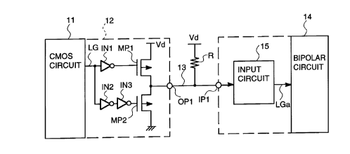
A first example of the invention is shown in Figure 2, in which an
integrated semiconductor circuit 11 consists of CMOS circuits. The circuit 11
outputs from its output circuit 12 a logic signal LG on a signal path 13, which is
connected to a power source of voltage Vd via a terminal resistor R provided
to adjust the impedance of the signal path 13 to a predetermined value.
CA 02062414 1998-0~-06
'_
The signal LG output from the CMOS circuit 11 is applied to
inverters IN1 and IN2 in the output circuit 12. The output of the inverter IN2 is
coupled to an inverter IN3.
The output of the inverter IN1 is connected to the gate of a p-
5 channel MOS transistor MP1. The output of the inverter IN3, which is invertedin logic level with respect to the output of the inverter IN2, is applied to the gate
of a p-channel transistor MP2.
The drain and the source of the p-channel MOS transistor MP1 is
connected to the power source of voltage Vd and to the drain of the p-channel
10 MOS transistor MP2, respectively.
The source of the p-channel MOS transistor MP2 is grounded.
The source of the p-channel MOS transistor MP1 and the drain of
the p-channel transistor MP2 are connected together to a common output
terminal OP1.
The output terminal OP1 of the output circuit 12 is connected to
one end of the signal path 13, the other end of which is connected to an input
IP1 of an input circuit 15. The output LGa of input circuit 15 is connected to an
integrated circuit 14 consisting of bipolar semiconductor circuits.
In this arrangement, a logic signal LG at low level L output from
20 the CMOS circuit 11 causes the inverter IN1 to output a logic signal high H and
causes the inverter IN3 to output a logic signal low L, which in turn cause the
p-channel transistor MP1 to be turned OFF, and MP2 to be turned ON.
The output circuit 12 is identical in function with an equivalent
circuit shown in Figure 3(a), which consists of a terminal resistor R, an ON-state
25 resistor R20n of the p-channel transistor MP2, a DC power source of voltage
DV2 representing the threshold voltage VTP2 for the p-channel MOS transistor
MP1, and a source voltage Vd, all connected in series between the power
source of voltage Vd and the ground.
If, on the other hand, the level of the logic signal LG of the CMOS
30 circuit 11 goes high H, the output of the inverter IN1 is changed to low L, while
CA 02062414 1998-0~-06
the output of the inverter IN3 is changed to high H. Accordingly, the p-channel
MOS transistor MP1 is turned ON and the transistor MP2 is turned OFF.
In this case the output circuit 12 is equivalent to a circuit shown in
Figure 3(b), which consists of an ON-state resistor R10n connected in parallel
with a terminal resistor R, between the power source of voltage Vd and the
output terminal OP1. Accordingly, when the logic signal LG is low L, the voltagelevel VlLp of the output terminal OP1 equals the threshold voltage VTP2 plus
the product of: (the power source voltage Vd minus the threshold voltage VTP2),
multiplied by (the ratio of the resistance of the ON-state resistor R20n to the
10 sum of the ON-state resistor R20n and resistor R, as shown in Figure 4(a).
On the other hand, when the output logic signal LG is high H, the
level VlHp of the output terminal OP1 is essentially the same as the power
source voltage Vd.
In the input circuit 15 a threshold level VIT is established for
15 identification of the logic high H by discriminating the level VlHp from the level
VlLp. To do this, the input circuit 15 is adapted to alter the logic level of the
output LGa from low L to high H. This occurs at time delay ta after the level ofthe output terminal OP1 of the output circuit 12 begins to rise from VlLp towards
the level VlHp in response to the change in logic state of the signal LG of the
20 CMOS circuit 11 from low L to high H, as shown in Figure 4 (b) and (c).
It should be noted that in the example described above the
amplitude of the signal on the signal path 13 is limited to a small range defined
by the levels VlLp and VlHp, so that the time delay ta is much smaller than a
conventional delay time, thereby permitting fast signal transfer.
In a typical example where the power source voltage Vd is 5 volts;
the terminal resistor, 50 ohms; and the threshold voltage VTP2 in the range
from 1.2 to 1.3 volts, the level VlLp will be in the range of 3 - 4 volts. One may
then set the threshold VIT at about 4.5 volts.
It should be appreciated that in the first example described above
30 the output signal of the CMOS circuit 11 may be input to the bipolar circuit 14
directly, the CMOS circuit 11 and the bipolar circuit 14 being manufactured so
CA 02062414 1998-0~-06
'~_
as to require no independent transistorized level converter circuit interfacing
them, thereby improving manufacturing cost of the integrated circuit.
Furthermore, since no extra space is needed for an independent level converter,
further downsizing of the integrated circuits may be achieved.
It should be also appreciated that the interconnection circuit above
has very stable operational characteristics. That is, the interconnection circuit
is little affected by ambient temperature and other conditions, since the outputstage of the circuit 12 is formed by the identical p-MOS transistors MP1 and
MP2 so that fluctuations of ambient conditions tend to cancel out each other in
these transistors. Fluctuations in quality of the transistors encountered duringmanufacture also tends to cancel out.
Referring now to Figure 5, there is shown a second example of the
invention, in which the same reference numbers/codes as in Figure 2 represent
the same or similar components.
A bipolar circuit 14 has two input terminals IP1 and IP2, which are
connected to the plus end and minus end, respectively, of a differential amplifier
16 provided in an input circuit 15. The output signal LGb of the differential
amplifier 16 is supplied as an input signal to a signal processing portion 15a of
the input circuit 15.
A reference signal generation circuit 17 includes a set of p-channel
MOS transistors MP3 and MP4, with the drain of the transistor MP3 connected
to a power source voltage Vd, the source of the transistor MP4 grounded, the
source of the transistor MP3 connected to the drain of the transistor MP4, and
the gates of the transistors MP3 and MP4 both grounded. Accordingly, the
transistors MP3 and MP4 are both always turned ON.
The reference signal generation circuit 17 also has another set of
p-channel transistors MP5 and MP6, with the drain of the transistor MP5
connected with the power source of voltage Vd, the source of the transistor MP6
grounded, and the source of the transistor MP5 connected with the drain of the
transistor MP6. The gate of the p-channel MOS transistor MP5 is grounded.
Accordingly, the transistor MP5 is always turned ON. The gate of the transistor
,~
CA 02062414 1998-0~-06
MP6 is connected to a node common to the source of the transistor MP3 and
the drain of the transistor MP4. The source of the transistor MP5 and the drain
of the transistor MP6 are connected to a common output terminal OP2 of the
reference signal generation circuit 17.
The output terminal OP2 is connected to an input IP2 of the bipolar
circuit 14, which input is the minus end of a differential amplifier 16. The
terminal OP2 provides a threshold voltage Vlth.
Figure 6(a) shows an equivalent circuit for the reference signal
generation circuit 17. The portion including the p-channel MOS transistors MP3
and MP4 is equivalent to a series of resistances R30n and R40n of ON-state
transistors MP3 and MP4, respectively, and a DC voltage VD4 representing the
threshold voltage VTP4 of the transistor MP4, all connected in that order
between the power source Vd and the ground.
As a result, the gate voltage of the transistor MP6 equals the sum
of the threshold voltage VTP4 and the product of: (the voltage Vd minus the
threshold voltage VTP4) multiplied by (the ratio of the ON-state resistance R40nto the sum of R30n and R40n).
Similarly, the portion including the p-channel transistors MP5 and
MP6 is equivalent to a series of a resistance R50n representing the ON-state
resistance of the p-channel transistor MP5, a resistance R60n representing the
ON-state resistance of the p-channel transistor MP6, and a DC voltage source
VD6 which is equal in magnitude to the gate voltage VTR of the transistor MP6,
all connected in that order between the power source Vd and the ground.
Accordingly, the threshold voltage Vlth is given by the sum of the
threshold voltage VTR and the product of: (the source voltage Vd minus the
threshold voltage VTR) multiplied by (the ratio of the resistance R60n to the
sum of R50n and R60n), as shown in Figure 6. Thus, by appropriately choosing
the values of the ON-state resistances R30n, R40n, R50n, and R60n, of the p-
channel transistors MP3, MP4, MP5, and MP6, respectively, the threshold
voltage Vlth may be set at a desired level.
CA 02062414 1998-0~-06
Therefore, as shown in Figures 7 (a) - (c), over a period when the
level of the output of the output circuit 12 remains below Vlth, the differential
amplifier 16 outputs a low level logic signal LGb to its signal processing portion
1 5a. On the other hand, over a period when the level of the output of the output
5 circuit 12 exceeds the threshold Vlth in association with the high output signal
LG of the CMOS circuit 11, the differential amplifier 16 outputs a high level logic
signal LGb to its signal processing portion 15a.
In the second example described above, the logic signal LGb
output from the differential amplifier 16 thus may switch from low L to high H at
10 time delay tb which is defined as the period required for the output terminal OP1
to reach the threshold level Vlth after the CMOS circuit 11 begins to alter its
output state.
It should be appreciated that in the second example the input
circuit 15 has large degrees of freedom for design parameters since the input
15 circuit 15 is provided with a threshold Vlth for use in discriminating the logic
levels, by an independent reference signal generation circuit 17. It should be
also appreciated that the reference signal generation circuit 17 consists only of
p-channel MOS transistors MP3, MP4, MP5, and MP6 and that the output stage
of the output circuit 12 consists of p-channel transistors MP1 and MP2, which
20 helps suppress variations in operational characteristics caused by changes in ambient conditions and manufacture non-uniformity, since these changes
influence the output levels of the output circuit 12 in the same direction and tend
to cancel out. The same is true in the reference signal generation circuit 17.
Referring now to Figure 8, there is shown a third example of the
25 invention, in which the same reference numbers/codes as in Figures 2 and 5
represent the same or similar components. As shown in the figure, the logic
signal LG output from a CMOS circuit 11 is supplied to inverters IN4 and IN5.
The output of the inverter IN4 is connected to the input of the inverter IN6.
The output of the inverter IN6 is connected to the gate of a p-
30 channel MOS transistor MP10. The output of the inverter IN5, which has an
CA 020624l4 l998-0~-06
'_
14
inverted level with respect to the inverter IN6, is connected to the gate of a p-
MOS transistor MP11.
The p-channel MOS transistor MP10 has its drain connected to a
power source voltage Vd, and its source connected to the drain of the transistor5 MP11. The source of the transistor MP11 is grounded. The source of the
transistor MP10 and the drain of the transistor MP11 are connected with each
other at a common node, to which is connected an output terminal OP3 of the
output circuit 12.
The output terminal OP3 is connected to one end of a signal path
18. The other end of the signal path 18 is connected to one terminal IP2 of a
bipolar circuit 14. The signal path 18 is also connected to a power source of
voltage Vd.
In this arrangement, if the CMOS circuit 11 outputs a logic signal
LG at low level L, the output of the inverter IN1 goes to high H, while the output
15 of the inverter IN3 goes to low L. Therefore, in this case the p-channel MOS
transistor MP1 is turned OFF, while the transistor MP2 is turned ON, bringing
the level of the output terminal OP1 to a level VlLp.
At the same time the output of the inverter IN6 goes to low L, while
the output of the inverter IN5 goes to high H. Accordingly, the p-channel
20 transistor MP10 is turned ON, and the transistor MP11 is turned OFF, bringing the level of the output terminal OP3 to a level VlHp.
However, if the CMOS circuit 11 outputs a logic signal LG at high
level H, the output of the inverter IN1 goes to low L, while the output of the
inverter IN3 goes to high H. Hence, the p-channel MOS transistor MP1 is
25 turned ON, while the transistor MP2 is turned OFF, bringing the output terminal
OP1 to the level VlHp.
At the same time the output of the inverter IN6 goes to high H,
while the output of the inverter IN5 goes to low L. Hence, the p-channel MOS
transistor MP10 is turned OFF, while the transistor MP11 is turned ON, bringing
30 the output terminal OP3 to the level VlLp.
CA 02062414 1998-0~-06
'',._
Accordingly, as shown in Figures 9 (a) - (c), as the logic level of
the signal LG of the CMOS circuit 11 changes from the level L to the level H,
the level of the output terminal OP1 of the output circuit 12 changes from the
level VlLp to the level VlHp, and the level of the output terminal OP3 from the
5 level VlHp to the level VlLp.
The outputs OP1 and OP3 are connected to the plus and minus
input terminals IP1 and IP2, respectively, of a differential amplifier 16 serving
as an input circuit for the bipolar circuit 14. The differential amplifier 16 thus
outputs to the signal processing portion 15a of the input circuit 15 a logic signal
10 LGc at low level L when the level of the output terminal OP1 is less than that
of the output terminal OP3.
As the level of the output terminal OP1 exceeds that of the output
terminal OP3, the differential amplifier 16 outputs to the signal processing
portion 15a a signal LGc at high level H.
In this manner, in the third example described above, the logic
signal LGc output from the differential amplifier 16 may switch from low L to
high H at delay time tc after the CMOS circuit 11 begins to alter its output LG
from low L towards high H. It should be noted that in the third example the
differential amplifier 16 provides the bipolar circuit 14 with an input signal which
is doubled in amplitude compared to the amplitude of the signal received from
the output circuit 12, so that influences of noise on the input signal may be
greatly reduced.
Figure 10 illustrates a fourth example of the invention, in which the
same reference numbers/codes as in Figure 2 represent the same or similar
components.
A CMOS circuit 21 consisting of CMOS transistors outputs a logic
signal LG from its output circuit 22 to a signal path 23, which path is connected
with a terminal resistor R for adjusting the impedance of the signal path 23.
The path 23 is also grounded. In an output circuit 22 the output signal LG from
the CMOS circuit 21 is applied to inverter circuits IN11 and IN12. The output
of the inverter circuit IN11 is connected to an inverter circuit IN13.
CA 02062414 1998-0~-06
16
The output of the inverter circuit IN13 is connected to the gate of
a n-channel MOS transistor MN1. The output signal from the inverter circuit
IN13 is inverted with respect to the output signal of the inverter circuit IN12, and
is applied to the gate of an n-MOS transistor MN2.
The drain of the n-channel MOS transistor MN1 is coupled to the
power source of voltage Vd. The source of the transistor MN1 is coupled to the
drain of the transistor MN2.
The source of the transistor MN2 is grounded. The source of the
transistor MN1 and the drain of the transistor MN2 are connected with each
other and with an output terminal OP11.
The output terminal OP11 of the output circuit 22 is connected with
one end of the signal path 23, while the other end of the signal path 23 is
connected with an input IP11 of the CMOS circuit 24 which consists of
integrated CMOS semiconductors. The input IP11 is connected with an input
terminal of the input circuit 25. The signal output from the input circuit 25 isapplied to the CMOS circuit 24 as an input logic signal LGd thereto.
In this construction the output of the inverter circuit IN13 goes low
L, and the output of the inverter circuit IN12 goes high H, when the CMOS
circuit 21 outputs a logic signal LG at level low L. Accordingly, the n-channel
MOS transistor MN1 is turned OFF, and n-channel MOS transistor MN2 turned
ON.
An equivalent circuit for the output circuit 22 is, as shown in Figure
11(a), an ON-state resistor R10n of the n-channel MOS transistor MN2
connected in parallel with the terminal resistor R between the ground and the
output terminal OP11.
The output of the inverter circuit IN13 goes high H, and the output
level of the inverter circuit IN12 goes low L, when the CMOS circuit 21 outputs
a logic signal LG at level high H.
Accordingly, the n-channel MOS transistor MN1 is turned ON, and
n-channel MOS transistor MN2 is turned OFF.
CA 02062414 1998-0~-06
'~_
In this case the output circuit 22 is equivalent to a circuit shown in
Figure 11(b), which is a series of a DC power source DN1 representing the
threshold voltage VTPN of the n-channel MOS transistor MN1, the ON-state
resistor r10n of the n-channel MOS transistor MN1, and the terminal resistor R,
5 all connected in that order between the power source of voltage Vd and the
ground.
Accordingly, when the output logic signal LG is low L, the output
terminal OP11 assumes a level VlLn which is substantially equal to the ground
level.
On the other hand, when the output logic signal LG is high H, the
output terminal OP11 assumes a level VlHn which equals the product of (the
power source voltage Vd minus the threshold voltage VTN1) multiplied by (the
ratio of the resistor R to the sum of the ON-state resistor r10n and the resistor
R), as shown in Figure 11(a).
Therefore, in order to discriminate the logic level high H from the
logic low L input in the input circuit 25, a threshold voltage VNth is set
intermediate between the levels VlLn and VlHn. Thus, as shown in Figure 12
(b) and (c), the output signal LGd of the input circuit 25 changes from low L tohigh H as the level of the output terminal OP11 of the output circuit 22 rises
20 from the level VlLn and reaches the intermediate level VNth in response to the
change in logic level of the output signal LG of the CMOS circuit 21 from its low
L to high H. This change takes a certain delay time td as shown in Figure
12(c).
Thus, in the fourth example the input logic signal LGd output from
25 the input circuit 25 changes to high H at delay time td after the alteration in logic
level of the output signal LG of the CMOS circuit 21.
Since the signal on the signal path 23 connected to the input
circuit 25 is limited in amplitude within a small range from VlLn to VlHn, delaytime td is significantly smaller than the prior art delay time, thereby permitting
30 fast signal transfer.
CA 02062414 1998-0~-06
In a typical example where the power source voltage Vd is 5 volts;
the terminal resistance R, 50 ohms; and the threshold voltage VTN1, in the
range 1.2 - 1.3 volts, the value of VlHn is approximately 2 volts. In this case
the threshold voltage VNth is preferably set in the range 1.3 - 1.5 volts.
5It should be noted that the output stage of the circuit 22 is
constituted by n-channel MOS transistors MP1 and MP2, which greatly helps
suppress variations in operational characteristics caused by varying ambient
conditions and manufacture non-uniformity; that is because those variations onlyinfluence the levels of the output circuit 12 and the reference signal generation
10circuit 17 in the same trend, and tend to cancel out.
Figure 13 illustrates a fifth example of the invention, in which the
same reference numbers/codes as in Figure 10 represent the same or similar
components.
In an output circuit 22 the signal LG, output from the CMOS circuit
1521, is applied to inverter circuits IN14 and IN15. The signal output from the
inverter circuit IN15 is applied to an inverter circuit IN16.
The output of the inverter circuit IN14 is coupled to the gate of a
n-channel MOS transistor MN3. The output signal of the differential amplifier
16 is inverted with respect to the output signal of the bipolar circuit 14, and is
20applied to the gate of a n-MOS transistor MN4.
The drain of the n-channel MOS transistor MN3 is coupled to a
power source of voltage Vd. The source of the transistor MN3 is coupled to the
drain of the transistor MN4. The source of the transistor MN4 is grounded. The
source of the transistor MN3 and the drain of the transistor MN4 are connected
25with each other and with an output terminal OP11.
In this construction the output of the inverter circuit IN14 goes high
H and the output of the inverter circuit IN16 goes low L when the CMOS circuit
21 outputs a logic signal LG at level low L. Accordingly, the n-channel MOS
transistor MN3 is turned ON, and n-channel MOS transistor MN2 is turned OFF.
30On the other hand, the output of the inverter circuit IN14 goes low
L and the output of the inverter circuit IN16 goes high H when the CMOS circuit
CA 02062414 1998-0~-06
-
19
21 outputs a logic signal LG at level high H. Accordingly, the n-channel MOS
transistor MN3 is turned OFF, and n-channel MOS transistor MN4 is turned ON.
Thus, in the example described, the level of the logic signal LG of
the CMOS circuit 21 is inverted with respect to the level of the logic signal LGe
5 of the input circuit 25, shown in Figure 14 (a), (b), and (c).
Referring now to Figure 15, there is shown a sixth example of the
invention, in which the same reference numbers/codes as in Figure 10 represent
the same or similar components.
A CMOS circuit 24 has an input circuit 25 including a differential
10 amplifier 26 and a signal processing portion 25a.
The plus and minus terminals of the differential amplifier 26
constitute the input terminals IP11 and IP12, respectively, for the circuit 24. The
signal output from the differential amplifier 26 is supplied to the signal
processing portion 25a as an input logic signal thereto.
A reference signal generation circuit 27 includes a set of n-channel
MOS transistors MN5 and MN6, with the drain of the transistor MN5 connected
to a power source of voltage Vd, the source of the transistor MN6 grounded, the
source of the transistor MN5 connected to the drain of the transistor MN6, and
the gates of the transistors MN5 and MN6 connected to the power source of
20 voltage Vd. Accordingly, both the transistors MN5 and MN6 are always turned
ON.
The reference signal generation circuit 17 also has another set of
n-channel transistors MN7 and MN8, with the drain of the transistor MN7
connected to the power source of voltage Vd, the source of the transistor MN8
25 grounded, and the source of the transistor MN7 connected with the drain of the
transistor MN8. The gate of the transistor MN8 is connected to the power
source Vd. Accordingly, the transistor MN8 is always turned ON. The gate of
the transistor MN7 is connected to a node common to the source of the
transistor MN5 and the drain of the transistor MN6, thereby allowing the gate to30 share the same voltage as the drain of the transistor MN6.
CA 02062414 1998-0~-06
The source of the transistor MN7 and the drain of the transistor
MN8 are also connected to a common output terminal OP12 of the reference
signal generation circuit 27.
The output terminal OP12 is connected to the input terminal IP12
of the CMOS circuit 24 to supply the minus terminal of the differential amplifier
26 with a threshold voltage VNth. Figure 16(a) shows an equivalent circuit for
the reference signal generation circuit 27. The portion including the n-channel
MOS transistors MN5 and MN6 is equivalent to a series of a DC voltage DN5
representing the threshold voltage VTN5 of the transistor MN5, and ON-state
resistances r50n and r60n of transistors MN5 and MN6, respectively, connected
in that order between the power source Vd and the ground. As a result, the
gate voltage of the transistor MN7 equals the source voltage Vd minus the
threshold voltage VTN5, multiplied by the ratio of the ON-state resistance r60n
to the sum of r50n and r6cn.
Similarly, the portion including the n-channel transistors MN7 and
MN8 is equivalent to a series of a DC voltage source equal in magnitude to the
gate voltage VRN of the transistor MN7, and ON-state resistances r70n and
r80n of the n-channel transistors MN7 and MN8, respectively, connected in that
order between the power source of Vd and the ground.
Accordingly, as shown in Figure 16(b), the threshold voltage VNth
is given by the source voltage Vd minus the voltage VRN, multiplied by the ratioof the resistance r80n to the sum of resistances r70n and r80n.
Thus, by appropriately choosing the values of the ON-state
resistances r50n, r60n, r70n, and r80n, of the n-channel transistors MN5, MN6,
MN7, and MN8, respectively, the threshold voltage VNth may be set at a
desired level.
As shown in Figure 17 (a) - (c), over a period when the level of the
output of the output circuit 22 remains below VNth, the differential amplifier 26
outputs a low level logic signal LGf to its signal processing portion 25a. On the
other hand, when the level of the output terminal OP11 exceeds the threshold
CA 02062414 1998-0~-06
'_
VNth, the differential amplifier 26 outputs a high level logic signal LGf to itssignal processing portion 25a.
Thus, in the sixth example described above the logic signal LGf
output from the differential amplifier 26 may switch from low L to high H at delay
time ff, which is defined as the time required for the output at terminal OP11 to
reach the threshold level VNth after the CMOS circuit 21 begins to alter its
output state from low L to high H.
It should be appreciated that the input circuit 25 has large degrees
of freedom for design parameters since the input circuit 25 is provided with a
threshold VNth generated by an independent reference signal generation circuit
27. It should be also appreciated that the reference signal generation circuit 27
consists only of n-channel MOS transistors MN5, MN6, MN7, and MN8, and that
the output stage of the output circuit 22 consists of n-channel transistors MN1
and MN2, which help suppress variations in operational characteristics caused
by changes in ambient conditions and manufacture non-uniformity; that is
because these variations influence the levels of the output signal of the outputcircuit 22 in the same direction and tend to cancel out. The same is true in thereference signal generation circuit 27.
Referring now to Figure 18, there is shown a seventh example of
the invention, in which the same reference numbers/codes as in Figures 10 and
13 represent the same or similar components.
A logic signal LG output from an output circuit 22 of a CMOS
circuit 21 is supplied to inverters IN11, IN12, IN14, and IN15. The output of the
inverter IN11 is connected to the input of the inverter IN13. The output of the
inverter IN15 is connected to the input of the inverter IN16.
The output of the inverter IN13 is connected to the gate of a n-
channel MOS transistor MN1. The output of the inverter IN12 is inverted with
respect to the output of the inverter IN13, and is connected to the gate of a n-channel MOS transistor MN2.
The n-channel MOS transistor MN1 has its drain connected to a
power source of voltage Vd, and its source connected to the drain of the
s~
CA 02062414 1998-0~-06
transistor MN2. The source of the transistor MN2 is grounded. The source of
the transistor MN1 and the drain of the transistor MN2 are connected with each
other and to an output terminal OP11.
The output of the inverter IN14 is connected to the gate of a n-
5 channel MOS transistor MN3. The output of the inverter IN16 is inverted withrespect to the output of the inverter IN14, and is connected to the gate of a n-
channel MOS transistor MN4.
The n-channel MOS transistor MN3 has its drain connected to the
power source of voltage Vd, and its source connected to the drain of the
10 transistor MN4. The source of the transistor MN4 is grounded. The source of
the transistor MN3 and the drain of the transistor MN4 are connected with each
other and to an output terminal OP13 of an output circuit of the CMOS circuit
21.
The output terminal OP13 is connected to an input terminal IP12
of a CMOS circuit 24 via a signal path 28. The signal path 28 is grounded via
a terminal resistor R, which is provided for setting the impedance of the signalpath 28 at a desired magnitude.
In this arrangement, if the CMOS circuit 21 outputs a logic signal
LG at low level L, the output of the inverter IN13 goes low L, while the output
20 of the inverter IN12 goes high H.
Therefore, the n-channel MOS transistor MN1 is turned OFF, while
the transistor MN2 is turned ON, bringing the level of the output terminal OP11
to a level VlLn.
At the same time the output of the inverter IN14 goes high H, while
25 the output of the inverter IN16 goes low L.
Accordingly, the n-channel transistor MN3 is turned ON, while the
transistor MN4 is turned OFF, yielding an output of voltage VlHn at the output
terminal OP13.
However, if the CMOS circuit 21 outputs a logic signal LG at a high
30 level H, the output of the inverter IN13 goes high H, while the output of theinverter IN12 goes low L. Hence, the n-channel MOS transistor MN1 is turned
,, ,~,
CA 02062414 1998-0~-06
-
ON, while the transistor MN2 is turned OFF, yielding an output of voltage VlLn
at the output terminal OP11.
At the same time the output of the inverter IN14 goes low L, while
the output of the inverter IN16 goes high H. Hence, the n-channel MOS
transistor MN3 is turned OFF, while the transistor MN4 is turned ON, yielding
an output of voltage VlLn at the output terminal OP13.
Accordingly, as shown in Figure 19 (a) - (c), as the CMOS circuit
21 alters the logic level of the signal LG from low L to high H, the level of the
output terminal OP11 of the output circuit 22 will be changed from VlLn to VlHn,10 and the level of the output terminal OP13 from the level VlHn to the level VlLn.
The output terminals OP11 and OP13 are connected, via input
terminals IP11 and IP12, respectively, to the plus and minus input terminals,
respectively, of a differential amplifier 26. The differential amplifier 26 thenoutputs to the signal processing portion 25a of the input circuit 25 of a CMOS
15 circuit 24 a logic signal LGg at low level L when the level of the output terminal
OP11 is less than that of the output terminal OP13.
As the level of the output terminal OP11 exceeds that of the output
terminal OP13, the differential amplifier 26 outputs to the signal processing
portion 25a a signal LGg at high level H.
In this manner, in the seventh example described above the logic
signal LGg output from the differential amplifier 26 may switch from low L to
high H at delay time tc after the CMOS circuit 21 begins to alter the level of its
output LG from low L to high H.
It should be noted that in the seventh example the differential
25 amplifier 26 provides the CMOS circuit 24 with an input signal which is doubled
in amplitude compared to the signal received from the output circuit 22, so thatinfluence of noise on the input signal may be greatly reduced.