Note: Descriptions are shown in the official language in which they were submitted.
-8994 2 0 624 63
SURFACE ACOUSTIC WAVE DEVICE FOR BAND-PASS FILTER
HAVING SMALL INSERTION LOSS AND PREDETERMINED
PASS-BAND CHARACTERISTICS FOR BROAD BAND
BACKGROUND OF THE INVENTION
l. Field of the Invention
The present invention relates to a surface
acoustic wave device, more particularly, to a surface
acoustic wave device used as a band-pass filter, etc.,
of mobile radio equipment, and the like.
2. Description of the Related Art
Recently, surface acoustic wave devices (which
may be abbreviated hereinafter as SAW devices) have been
developed and provided for RF circuit integrations of
communication equipment such as mobile telephone
transceivers, cable TV repeaters and converters, and the
like.
The SAW device comprises a piezoelectric
substrate and inter-digital transducers (which may be
abbreviated hereinafter as IDTs) disposed thereon for
converting a voltage into a surface acoustic wave, or a
surface acoustic wave into a voltage. Note, the SAW
device including IDTs converts a high-frequency voltage
into a surface acoustic wave having a wavelength of
about l0- 5 times. The wave is propagated on the
surface of the piezoelectric substrate and again
converted into a voltage by the IDTs.
The SAW device provides a filter function for
selecting frequencies by the above described double
conversion and depending on the shapes of the IDTs.
Note, the SAW device can cause the surface acoustic
waves to resonate by using a plurality of the IDTs, or
reflectors for reflecting surface acoustic waves beside
the IDTs. Namely, the SAW device may provide a
resonator function. Since the SAW device can delay
propagation speed to about l0-5 times the speed of an
T
_ - 2 - 2062~3
electromagnetic wave, it may serve as a delay device.
These functions of the SAW devices are
applicable for realizing filters, resonators, delay
lines, etc., which are compact, inexpensive, and
adjustment free. For example, they are used for
intermediate frequency (IF) filters, resonators of
oscillators, voltage control oscillators (VCOs), etc.
These days, the SAW devices are operated at higher
frequencies, and because they are compact and
inexpensive, they are also used for band-pass filters
for mobile radio equipment such as automobile and
portable telephone equipment. Therefore, the SAW
devices are required to have a small insertion loss and
predetermined pass-band characteristics for a broad
band.
SUMMARY OF THE INVENTION
An object of the present invention is to provide a
surface acoustic wave device to suppress ripples and
realize predetermined pass-band characteristics for a
broad band. Further, another object of the present
invention is to provide a surface acoustic wave device
to reduce the insertion loss thereof.
According to the present invention, there is
provided a surface acoustic wave device comprising: an
input terminal; an output terminal; a first multiple-
electrode surface acoustic wave element including a
plurality of first inter-digital transducers and second
inter-digital transducers alternating with each other,
and the first inter-digital transducers being connected
to the input terminal; and a second multiple-electrode
surface acoustic wave element including a plurality of
third inter-digital transducers and fourth inter-
digital transducers alternating with each other, the
first and second multiple-electrode surface acoustic
wave elements being mirror-symmetrically arranged and
disposed on a piezoelectric substrate, the third inter-
digital transducers being connected to the output
2062463
~_ - 3 -
terminal, and the fourth inter-digital transducers
being connected to the second inter-digital transducers;
wherein the number of the first or third inter-digital
transducers is equal to or smaller by one, than the
number of the second or fourth inter-digital transducers
The surface acoustic wave device may further
comprise at least one reflector for reflecting surface
acoustic waves being disposed outwardly from the
outermost of the first and third inter-digital
transducer; a center distance d between the first and
second inter-digital transducers or the third and
fourth inter-digital transducers being determined to be
d = (n+~ ) A , where, A being intervals of teeth
of each inter-digital transducer, n being an optional
integer, and ~ ranging from 0.17 to 0.25; and a center
distance d' beween the reflector and the outermost of
the first and third inter-digital transducer is
determined to be d' = n A or d' = (n+1/2)- A . The
reflector may be constituted by a inter-digital
transducers or strip electrodes.
The surface acoustic wave device may further
comprise at least one fifth inter-digital transducers
disposed outwardly from the outermost second inter-
digital transducers, and at least one sixth inter-
digital transducers disposed outwardly from theoutermost fourth inter-digital transducers; a center
distance between the fifth or sixth inter-digital
transducer and the second or fourth inter-digital
transducer is determined to be d' = n- A or d' =
(n+1/2)- A . The fifth inter-digital transducer and
the sixth inter-digital transducer may be connected to
each other to form connected electrodes.
BRIEF DESCRIPTION OF THE DRAWINGS
The present invention will be more clearly
understood from the description of the preferred
embodiments as set forth below with reference to the
accompanying drawings, wherein:
20s2~
~_ - 4 -
Figure 1 is a view showing an example of an
electrode configuration of a SAW device according to
the prior art;
Figure 2 is a view showing another example of
an electrode configuration of a SAW device according to
the prior art;
Figure 3 is a view showing band characteristics
of the SAW devices shown in Figs. 1 and 2;
Figure 4 is a view showing a relationship
between the total number of electrodes and insertion
loss thereof;
Figure 5 is a view showing an electrode
configuration of a first embodiment of a SAW device
according to the present invention;
Figure 6 is a view showing an electrode
configuration of the modification of the SAW device
shown in Fig. 5;
Figure 7 is a view showing band characteristics
of the SAW device shown in Fig. 6;
Figure 8 is a view showing a relationship
between the total number of electrodes and an
output/input power ratio;
Figure 9 is a view showing a relationship
between the total number of electrodes and insertion
loss thereof;
Figure lO is a view schematically showing an
example of the SAW device according to the related art;
Figure 11 is a view showing a unit in the SAW
device of Fig. lO;
Figure 12 is a view showing pass-band
characteristics of the filter, i.e., the SAW device of
Fig. lO;
Figure 13 is a view showing a waveform of
impulse response of a SAW device;
Figure 14 is a view explaining an impulse
response in a SAW device;
Figures 15A to 15C are views showing a
2062~63
relationship between the phase of a primary response
wave and those of delayed waves in a SAW device;
Figure 16 is a view showing pass-band
characteristics after Fourier transformation of the
impulse response of Figs. 15A to 15C;
Figure 17 is a view showing pass-band
characteristics of the impulse response of Figs. 15A to
15C with the phase of the first delayed wave being the
same as that of the primary response wave;
Figure 18 is a view schematically showing a
second embodiment of a SAW device according to the
present invention;
Figure 19 is a view schematically showing a
modification of the second embodiment of the SAW device
shown in Fig. 18;
Figures 20A and 20B are views showing filter
pass-band characteristics of SAW devices of the present
invention and the related art;
Figures 21A and 21B are views showing impulse
responses based on the filter characteristics of the
SAW devices of the present invention and the related
art; and
Figure 22 is a view showing an example of
mobile radio equipment using SAW devices.
DESCRIPTION OF THE PREFERRED EMBODIMENTS
For a better understanding of the preferred
embodiments, first, the problems of the prior art will
be explained, with reference to Figs. 1 to 4.
Figure 1 shows an example of an electrode
configuration of a SAW device (surface acoustic wave
device) according to the prior art, and Fig. 2 shows-
another example thereof. Note, the SAW device of Fig.
1 is an example of a multiple-electrode configuration
(with reference to "SAW Filters Employing Interdigitated
Interdigital Transducers, IIDT", M. Lewis, 1982,
Ultrasonics Symposium Proceedings, p.12), and the SAW
device of Fig. 2 is an example of a cascaded multiple-
_ - 6 - ~o62~3
electrode configuration (with reference to Institute of
Electronics, Information and Communication Engineers of
Japan, Technical Study Report, US81-22, p. 25, or "High
Performance SAW Filters with Several New`Te`chnologies
for Cellular Radio", M. Hikita et al., 1984, Ultrasonics
Symposium Proceedings, p.82).
Each figure shows the electrode configuration but
omits piezoelectric substrates, etc. Further, in Figs.
1 and 2, IDTs (inter-digital transducers, or comb
shaped electrodes) are of a so-called normalized type,
and the numbers of meshing inter-digital transducer
teeth pairs are not precise.
In Fig. 1, references lA to 5A denote IDTs each
having a smaller number of meshing electrode teeth
pairs, and lB to 4B denote IDTs each having a larger
number of meshing electrode teeth pairs. As shown in
Fig. 1, five electrodes lA to 5A and four electrodes lB
to 4B are alternately arranged to provide nine
electrodes in total with five inputs and four outputs.
At each side of a row of the electrodes, there is
arranged a reflector lC, 2C such as a short strip
reflector. Note, the electrodes lA to 5A are connected
to an input terminal IN, and the electrodes lB to 4B are
connected to an output terminal OUT, thereby forming a
multiple-electrode SAW device 1, e.g., a multiple-
electrode surface acoustic wave filter.
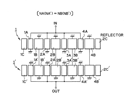
As shown in Fig. 2, the multiple-electrode SAW
device (SAW element) 1 comprising five inputs and four
outputs and a multiple-electrode SAW device ~SAW
element) 1' identical to the device 1 are mirror-
symmetrically arranged. Note, opposing IDTs lB to 4B
of the SAW device 1 and opposing IDTs lB' to 4B' of the
SAW device 1' are connected to each other. Further,
the IDTs lA to 5A of, for example, the multiple-
electrode SAW device 1 serve as an input end (IN), andthe IDTs lA' to 5A' of the other SAW device 1' serve as
an output end (OUT). Namely, the SAW devices (SAW
_ _ 7 _ 2 0624 63
elements) l and l' are cascaded to form a multiple-
electrode SAW device.
In Fig. 2, arrows denote directions of surface
acoustic waves converted from electric signals by the
IDTs, or electric signals converted from surface
acoustic waves.
Figure 3 shows band characteristics of the SAW
devices shown in Figs. l and 2. In Fig. 3, an ordinate
represents insertion loss (dB) and an abscissa
represents a frequency (MHz). Note, the samples shown
are based on a multistage electrode arrangement of
normalized 7-input 6-output type, formed on a 36 Y-X
LiTaO3 substrate. Further, an A-electrode (input/output
electrode: lA, 2A, --) is constituted by 22-pair
electrodes (split-fingers), a B-electrode (connected
electrodes: lB, 2B, --) is constituted by 30-pair
electrodes (split-fingers), and a reflector (lC, 2C, --) is
determined as 30-pair short strip type reflector.
In Fig. 3, reference numeral (l) represents the
characteristics of the multiple-electrode configuration
of Fig. l, and (2) represents those of the cascaded
multiple-electrode configuration of Fig. 2.
The multiple-electrode configuration partly shows
insufficient attenuation in a blocking zone. On the
other hand, the cascaded multiple-electrode
configuration shows excellent attenuation in the
blocking zone, thereby providing the surface acoustic
wave filter with excellent blocking characteristics.
In the conventional multistage SAW devices, the
cascaded multiple-electrode configuration may greatly
improve the attenuation characteristics in the blocking
zone, but increase insertion loss to 6 dB or more in a
pass-band to exceed an allowable range of, for example,
automobile and portable telephone sets that require a
low loss (for example, 4 to 5 dB).
Figure 4 shows a relationship between the total
number of electrodes and insertion loss thereof. In
_ - 8 - 2062~ 63
Fig. 4, an ordinate represents the insertion loss, and
an abscissa represents the total number of electrodes.
Values shown have been calculated with no regard to
surface acoustic wave propagation loss on a
piezoelectric substrate nor to a IDT resistance loss.
When increasing the total number (S) of electrodes
S = NA + NB, the insertion loss is decreased. Note, the
reference NA denotes the number of IDTs A (A-
electrodes) on the input side, and NB denotes the number
of IDTs B (B-electrodes) on the output side of the
multiple-electrode configuration. As shown in Fig. 4,
approximately at S = 13 with 7 inputs and 6 outputs, a
decrease in the insertion loss becomes flat. Namely,
when the total number S of electrodes is larger than 13,
the insertion loss does not decrease significantly. On
the other hand, when increasing the total number S of
electrodes, the size of the substrate continues to
increase. Accordingly, increasing the total number S of
electrodes alone does not effectively decrease the
insertion loss in practical use. This problem must be
solved.
Below, the preferred embodiments of a SAW device
according to the present invention will be explained,
with reference to the accompanying drawings.
Figure 5 shows an electrode configuration of a
first embodiment of a SAW device (surface acoustic wave
device) according to the present invention, and Fig. 6
shows an electrode configuration of the modification of
the SAW device shown in Fig. 5. Note, in Fig. 5, the
number of IDTs ( inter-digital transducers) A on input
(NA) equals to the number of IDTs B on output (NB), i.e.,
NA = NB; and in Fig. 6, the number of IDTs A on input
(NA) equals the number of IDTs B on output ( NB) minus
one, i.e., NA = NB - 1. Further, references NA' and
NB' represent the numbers of IDTs A and B of another
(1') of the multiple-electrode surface acoustic wave
elements that are mirror-symmetrically arranged. In
2062463
g
addition, NA = NA' and NB = NB'.
In Figs. 5 and 6, only the configuration of the
electrodes are described, and the piezoelectric
substrate and the like are not shown. In Figs. 5 and 6,
reference numerals l and l' denote a pair of multiple-
electrode surface acoustic wave elements (SAW elements)
that are mirror-symmetrically arranged. The
input/output IDTs A are connected to input terminal IN
and output terminal OUT, and opposing connected IDTs B
Of the two elements are connected to each other. Note,
references lC, 2C, lC', and 2C' denote reflectors.
As shown in Fig. 5, in the case of NA = NA' = NB =
NB' = 4 (a 4-input 4-output configuration), the SAW
element 1 comprises four input/output electrodes (IDTs)
lA, 2A, 3A, 4A and four connected electrodes (IDTs) lB,
2B, 3B, 4B, and the SAW element l' comprises four
input/output electrodes lA', 2A', 3A', 4A' and four
connected electrodes lB', 2B', 3B', 4B'.
On the other hand, as shown in Fig. 6, in the case
of NA = NA' = NB - l = NB' - l = 4 (a 4-input 5-output
configuration), the SAW element 1 comprises four
input/output electrodes (input IDTs) lA, 2A, 3A, 4A and
five connected electrodes (connected IDTs) lB, 2B, 3B,
4B, 5B, and the SAW element l' comprises four
input/output electrodes (output IDTs) lA', 2A', 3A',
4A' and five connected electrodes (connected IDTs) lB',
2B', 3B', 4B', 5B'. Note, the IDT (input/output
electrode or connected electrode) is constituted by a
plurality of pair electrodes (split-fingers), which
will be explained in detail with reference to Fig. ll.
Figure 7 shows band characteristics of the SAW
device shown in Fig. 6. In Fig. 7, an ordinate
represents insertion loss (dB), and an abscissa
represents a frequency (MHz).
A piezoelectric substrate used for the sample is a
36 Y-X LiTaO3 single-crystal substrate, and the size of
the device is 1.2 mm X 2.2 mm with 0.5 mm thick.
2062463
-- - 10-
An Al-Cu (0.2%) film for forming IDTs is deposited
in a vacuum with a thickness of 100 nm. According to a
known photolithography technique, a surface acoustic
wave filter for an 800 MHz band is formed with an
electrode pitch of 2.45 ~ m, an electrode width of
1.23 ~ m, and an electrode space of 1.23 ~ m.
The electrodes are arranged at NA = NA' = NB - 1 =
NB' - 1 = 6 in a 6-input 7-output configuration. The
total number of electrodes is S = 13. The IDTs A and B
are each a normalized type. Note, the number of
electrode teeth pairs of the IDT A (lA, 2A, --) is 22,
and that of the IDT B (lB, 2B, --) is 30. Further, the
reflector C (lC, 2C, --) is a 30-pair open strip
reflector.
The device of the present invention described above
is packaged in a metal case such as TO-48 (not shown),
and its frequency characteristics are measured with a
network analyzer. Note, the TO-48 is an example of
metal cans used to enclose various electronic elements.
As described above, the SAW device of the first
embodiment of the present invention comprises a pair of
mirror-symmetrically arranged multiple-electrode
surface acoustic wave elements disposed on a
piezoelectric substrate. Each of the elements involves
a plurality of IDTs A and B alternating with each other.
Opposing IDTs B of the pair are connected to each other.
The IDTs A of one of the elements form an input end
input terminal IN), and the IDTs A of the other element
form an output end (output terminal OUT). The number
(NA) of the IDTs A is equal to or smaller by one than
the number (NB) of the IDTs s.
As shown in the figures, the surface acoustic wave
filter (SAW filter) according to the first embodiment of
the present invention achieves insertion loss of 3 to 5
dB, i.e., an improvement of about 1 dB compared with
the prior art. This sufficiently meets the allowable
range of the automobile and portable telephone sets that
- 11- 2062463
require a low insertion loss.
Next, characteristics of the SAW devices between
the present invention and the prior art will be
explained with reference to Fig. 8 and 9.
Figure 8 shows a relationship between the total
number of electrodes and an output/input power ratio,
and Fig. 9 shows a relationship between the total
number of electrodes and insertion loss thereof.
When the number of IDTs A oriented in a surface
acoustic wave propagation direction is NA and that of
the IDTs B is NB, the arrangement of Fig. 2 will be a
5-input 4-output configuration with NA = 5 and NB = 4.
Namely, the conventional electrode configuration is
expressed as follows:
NA = NB + 1 ----- ( I )
Electro-mechanical energy conversion carried out in
each IDT may be understood as a 3-terminal conversion
system. When one piece of energy is provided to one of
the terminals, the other two terminals convert the
energy and each provide 1/2 of the energy (with
reference to N. Sakamoto et al., "Surface Acoustic Wave
(SAW) Filter", Electronics Material, p. 120, May, 1988).
For example, in the SAW device shown in Fig. 2,
when one piece of electric power is supplied to the
upper input terminal IN, the five input IDTs lA to 5A
(input/output electrodes A) receive 1/5 of the electric
power, respectively. These IDTs lA to 5A convert the
electric power into surface acoustic waves, and each
side of each of the IDTs lA to 5A emits 1/10 of the
electric power. At this time, the surface acoustic
waves of 1/10 power emitted from the outer side of the
outermost IDTs lA and 5A are not directly received by
the connected IDTs lB and 4B, and are wasted as a loss.
Namely, 2/10 of the power emitted from the left and
right sides are wasted.
Note, each side of each connected IDTs lB to 4B
(connected electrodes B) receives the surface acoustic
2062463
- 12-
waves of l/l0 power and converts it into electric power
and thus each IDT (lB to 4B) then transmits 2/l0 of the
electric power in total to the connected IDTs lB' to 4B'
in the second row (l').
Thereafter, each side of each connected IDT ( lB' to
4B') provides a surface acoustic wave of l/l0 power.
Note, each of the outermost IDTs lA' and 5A' receives
the surface acoustic wave only from one side, l/20 of
the power is lost, and only l/20 of the surface
acoustic wave is converted into electric power and
transmitted to the output end (output terminal). The
other inside output IDTs 2A' to 4A' receive the surface
acoustic wave power from both sides thereof, so that
each may provide 2/l0 of the electric power.
These pieces of power are collected at the output
terminal OUT, which finally provides 7/l0 of the
electric power. The total loss, therefore, will be 3/l0
of the electric power. This will be expressed with the
following general equation ( I ):
P = (2NA - 3) / 2NA ----- (~ )
Where, the total number (S) of electrodes S = NA +
NB and NA = NB + l are established, and the equation (~ )
becomes as follows:
P = (S - 2) / (S + l) ----- (m )
On the other hand, according to the present
invention, the number (NA) of the IDTs A is equal to or
smaller than the number (NB) of the IDTs B. That is:
NA = NB (with reference to Fig. 5) ----- (~ )
or
NA = NB - l (with reference to Fig. 6) ----- (V )
Electric power provided from the output terminal
OUT with respect to one piece of power supplied to the
input terminal IN is expressed with the following
equations (~ ) and (~ ):
P = (4S - 9) / 4S
P = (2S - 5) / (2S - 2) .......... (~ )
Figure 8 shows a relationship between the total
2062463
_ - 13-
number of electrodes and an output/input power ratio,
which is based on these three equations ( m ), (~ ), and
(~ill ).
In Fig. 8, an ordinate represents an output/input
power ratio (P), and an abscissa represents the total
number of electrodes (S). Note, similar to Fig. 4,
values have been calculated with no regard to a surface
acoustic wave propagation loss on a piezoelectric
substrate, and the like. Further, in Fig. 8, curves
(1) and (2) relate to the present invention, and the
curve (1) is for NA = NB and the curve (2) for NA = NB
- 1. In addition, a dotted curve (3) is the
conventional case of NA = NB + 1 for comparison
purposes.
As shown in Fig. 8, each case of the present
invention shows an improvement in the output/input power
ratio P compared with the prior art.
Figure 9 shows a relationship between the total
number of electrodes and insertion loss thereof. In
Fig. 9, an ordinate represents insertion loss, and an
abscissa represents the total number of electrodes.
When the total number S of electrodes is in a range
of from 5 to 13, the present invention reduces the
insertion loss less than the prior art by 0.5 to 1 dB.
When the total number of electrodes increases beyond a
point, the insertion loss reducing effect does not
improve in proportion to the increase in the device size.
The total number S, therefore, is in practice up to
about 13.
Note, the above embodiments are only examples.
Without departing from the scope of the present
invention, the numbers of electrodes, electrode teeth
pairs and reflectors, the material of the electrodes,
and the frequency bands may change for optimum
designing.
Figure lO shows an example of the SAW device
according to the related art corresponding to the SAW
20~2~63
_ - 14-
device shown in Fig. 6, which achieves high attenuation
in blocking zones at low loss. Nevertheless, the SAW
device is not sufficiently effective in reducing ripples
in a band.
As shown in Fig. l0, the SAW device comprises two
SAW elements 1 and l' which are mirror-symmetrically
arranged and disposed on a piezoelectric substrate (for
example, 36 Y-X LiTaO3 substrate). The SAW element l
comprises six input/output electrodes (input IDTs) lA to
0 6A and seven connected electrodes (connected IDTs) lA
to 7B, and the SAW element l' comprises six
input/output electrodes lA' to 6A' ( output IDTs) and
seven connected electrodes lB' to 7B' (connected IDTs).
Note, the IDT ( input/output electrode or connected
electrode) is constituted by a plurality of pair
electrodes.
Figure ll shows a unit in the SAW device of Fig. l0.
As shown in Fig. ll, each unit l0 of the SAW device
comprises split-finger (comb) shape patterns l0a, l0b
formed from a spattered aluminum-copper (Al-Cu) film
(having a thickness of, for example, l000 angstroms:
~ ) on a lithium tantalate (LiTO3) piezoelectric
crystalline material. Note, the LiTOa is specified to
a 36 rotation Y cut X propagation LiTaO3 single-ecrystal
substrate (36 Y-X LiTaO3 substrate), 41 Y-X LiNbO3
substrate, 64 Y-X LiNbO3 substrate, and the like.
When the unit l0 is determined to be an input IDT A
(lA to 6A), the upper split-finger electrode l0a is
connected to an input terminal and the lower split-
finger electrode l0b is connected to the grounded, and
when the unit l0 is determined to be an input IDT A'
(lA' to 6A'), the upper split-finger electrode l0a is
connected to the ground and the lower split-finger
electrode l0b is connected to an output terminal. Note,
the unit l0 of Fig ll is described when the unit l0 is
determined to be the input IDT lA of the SAW device
shown in Fig. l0. Further, when the unit l0 is
- 2062~63
_ - 15-
determined to be a connected IDT B (lB to 7B) of the
upper SAW element l, the upper split-finger electrode
lOa is connected to the ground and the lower split-
finger electrode lOb is connected to an upper electrode
(lOa) of the corresponding connected ID~ B' (lB' to
7B') of the lower SAW element l', and when the unit lO
is determined to be a connected IDT B' (lB' to 7B') of
the lower SAW element l', the upper split-finger
electrode lOa is connected to a lower electrode (lOb) of
the corresponding connected IDT B (lB to 7B) of the
upper SAW element l, and the lower split-finger
electrode lOb is connected to the ground.
As shown in Fig. ll, a tooth width (EL ), a space
(E5 ) between teeth (or adjacent fingers), and a teeth
pitch (ED ) of the IDT (unit lO) are usually designed
as EL = ES = A /4 and ED = A /2, where A is the
wavelength of a surface wave. To obtain a center
frequency of 835 MHz, for example, A is calculated as
4.9 Jlm from a sound velocity of 4090 m/sec. for an X-
propagation surface wave on the substrate. The pitch EDof electrode teeth may be 2.45 ~Im, and the electrode
tooth width EL and space E5 may be 1.23 ~ m,
respectively.
As described above, usually, a pair of input/output
IDTs are arranged opposite each other. Automobile and
portable telephone sets require surface acoustic wave
filters achieving a low loss (for example, insertion
loss of 3 to 5 dB or lower), a wide band (for example,
a center frequency of 835 MHz or greater and a pass-band
width of 25 MHz or greater), and an excellent degree of
suppression (for example, an out-of-band attenuation of
24 to 25 dB).
As described above, as shown in Fig. lO, the SAW
device comprises six input/output IDTs A (lA to 6A, lA'
to 6A') (each with, for example, 22 pairs of IDT teeth),
and seven connected electrodes B (lB-lB' to 7B-7s')
(each with, for example, 30 pairs of IDT teeth). Along
2062463
~ - 16-
-
the outer sides of the connected electrodes (lB-lB',
7B-7B'), there are arranged four reflectors C (lC, lC',
2C, 2C') for reflectinq surface acoustic waves. As is
apparent in Fig. 10, the IDTs lA to 6A, the connected
electrodes lB to 7B, and reflectors lC and 2C are
mirror-symmetrically arranged with respect to the IDTs
lA' to 6A', the connected electrodes lB' to 7B', and
reflectors lC' and 2C' along a straight line L.
In Fig. 10, a center distance between the
input/output IDT A and the connected electrode B, e.g.,
a center distance d between the input/output IDT 6A
(6A') and the connected electrode 7B
(7B') is d = (30+1/4)- ~ = 30.25A . A center distance
between the connected electrode B and the reflector C,
e.g., a center distance between the connected electrode
7B (7B') and the reflector 2C (2C') is equal to the
center distance d between the input/output IDT A and the
connected electrode B.
Figure 12 shows pass-band characteristics of the
filter, i.e., the SAW device of Fig. 10. To clearly
show ripples, the pass-band characteristics of the
filter (SAW device) are measured without any impedance
matching alignment.
As shown in Fig. 12, the pass-band characteristics
of the SAW device (filter) of Fig. 10 involve ripples
of about 2.5 dB in a pass-band. Such large ripples in
the pass-band characteristics of the filter fluctuate
gains from channel to channel in a band used for, for
example, mobile radio equipment. This is undesirable.
As disclosed in, for example, Japanese Unexamined
Patent Publication (Kokai) No. 3-270309, ripples
occurring in a band are caused by delayed waves (echo
waves). Generally, a multiple-electrode filter (SAW
device), which is a subject of the present invention,
successively receives delayed waves after a primary
response wave.
Figure 13 shows a waveform of impulse response of a
2062~63
SAW device, and Fig. 14 shows an impulse response in a
SAW device.
In Fig. 13, an output terminal OUT of the SAW
device of Fig. 14 provides a primary response (wave) WO
and echo waves such as a first delayed wave W, after a
time Tl~ a second delayed wave W2 after a time r 2, a
third delayed wave W3 after a time r 3 ~ and the like.
These echo waves are electric responses appearing at the
output terminal OUT of the SAW device shown in Fig. 14,
when an impulse voltage is applied to an input terminal
IN of the SAW device.
The echo waves W,, W2, W3 ~ -- are produced by the
multiple reflection and transmission of surface
acoustic waves between IDTs. As shown in Fig. 14, for
example, a surface acoustic wave produced by an input
IDT ( input electrode) 2A is propagated to the left and
right. The right one passes along a route Pl and
reaches a connected IDT ( connected electrode) 3B, which
converts the wave into an electric signal. The
electric signal passes along a connection route P2 and
reaches a connected IDT 3B', which converts the signal
into a surface acoustic wave again. Note, the surface
acoustic wave is emitted from each side of the input IDT
2A. The wave transmitting along a route P3 through the
connected IDT finally reaches an output IDT 2A', so
that the output terminal OUT of the SAW device provides
an electric signal. This is the shortest response to
the impulse and corresponds to the primary response
wave WO. Note, there are many routes other than those
mentioned above for the primary response (wave). The
primary response involves the largest amplitude to
provide the primary response wave W0 of Fig. 13.
There are also many routes for the first delayed
wave Wl. Among them, Fig. 14 shows (1) a route of P4
P2 P8 (multiple reflection between the input IDT 2A
and the connected IDT 3B), (2) a route of Ps ~ P2 P3
(a wave is transmitted through the connected IDT 3B,
_ - 18- ~2~63
reflected by an input IDT 3A, returned to the connected
IDT 3B, and transmitted from the IDT 3B' to the output
IDT 2A'), and ( 3) a route of P, P8 ~ P8 (a wave is
transmitted through the connected IDT 3B and the input
IDT 3A, received by a connected IDT 4B, and transmitted
from a connected IDT 4B' to an output IDT 3A'). All of
them involve the same time delay (for example Tl)-
Waves that pass through a first filter along the
shortest route (time) and transmit through or are
repeatedly reflected by a second filter will become
delayed waves involving the same delay. These waves
overlap one upon another to form the first delayed wave
Wl. The amplitude of the first delayed wave Wl is
smaller than that of the primary response because of
reflection and transmission. The delay time T I is
obtained from the following equation:
r , = 2- d/V
= 2- (n+~ /V = 2- (n+~ )- T 0 -- (a)
where d is a center distance between the IDTs, V is an
average sound velocity for d, n is an integer, ~ is a
real number smaller than 1, and T 0 is a propagation
time for intervals of the IDTs, corresponding to a
reciprocal of a resonant frequency fO.
Similarly, there are many routes for the second
delayed wave W2. The amplitude of this wave is further
smaller, and its delay time T 2 is twice the delay
time r 1. The third and following delayed waves (W3,
--) successively appear at intervals of Tl. Note,
usually, these delayed waves are undesirable because
they cause ripples in a pass-band, and many efforts
have been made to suppress these undesirable waves.
Further, Japanese Unexamined Patent Publication (Kokai)
No. 3-270309 explains, however, that these undesirable
waves can be utilized to extend a band.
Figures 15A to 15C show a relationship between the
phase of a primary response wave and those of delayed
waves in a SAW device, and Fig. 16 shows pass-band
2062463
- _ - 19-
characteristics after Fourier transformation of the
impulse response of Figs. 15A to 15C.
According to the waveform of Fig. 15A
(corresponding to the impulse response waveform of Fig.
13), the phases of the first, third, -- delayed waves
Wl ~ W3 ~ i.e-, odd order delayed waves are opposite
to that of the primary response wave W0 (Fig. 15B), and
the phases of even order delayed waves W,, Wl, -- are
the same as that of the primary response wave W0 (Fig.
15C). Therefore, the filter (SAW device) realizes flat
pass-band characteristics as shown in Fig. 16.
Figure 17 shows pass-band characteristics of the
impulse response of Figs. 15A to 15C with the phase of
the first delayed wave being the same as that of the
primary response wave.
When the phases of the odd order delayed waves W,,
W,, -- are the same as that of the primary response wave
W~, the pass-band characteristics show a mountain-like
shape as shown in Fig. 17. Namely, the pass-band
characteristics are not flat. To obtain good pass-band
characteristics, it is necessary to invert the phases of
the odd order delayed waves Wl, W3 ~ -- with respect to
that of the primary response wave W0. To realize this,
a distance d between IDTs must be determined to be (n+
~ ) ~ (where, ~ is defined from 0.17 to 0.25).
Accordingly, a term of 2 ~ appears for T, in the
equation (a), so that, when ~ is 1/4 (=0.25), a term
of 1/2 (= 0.5r 0) is added, and the phases of the odd
order delayed waves Wl, W3 ~ -- become opposite to that
of the primary response wave WO. Actually, it has been
experimentally confirmed that this effect appears when
ranges from 0.17 to 0.25.
As shown in Fig. 16, the pass-band will be flat
when the delayed waves involve proper amplitudes (for
example, the electric power of the first delayed wave
is determined to be about 1/10 that of the primary
response) and a proper time delay (for example, a
~ - 20- 2062463
reciprocal of T I is determined to be approximately
equal to a required band width). If the amplitudes of
the delayed waves are unnecessarily large, undesirable
ripples will appear in the flat pass band. It is
necessary, therefore, to provide a means for properly
controlling the amplitude of the first delayed wave Wl.
Among the delayed waves (echo waves), the first delayed
wave Wl has the largest amplitude, so that it
inadvertently influences the pass-band. If the first
delayed wave Wl is controllable, the ripples in the
band can be reduced to an extent causing no problem in
actual use.
Consequently, a delayed wave of the same phase is
slightly added to a delayed wave of an opposite phase,
to adjust the magnitude (amplitude) of the first delayed
wave Wl. At this time, adjusting the amplitude of the
first delayed wave W~ must not influence the amplitude
of the primary response wave WO. If the amplitude of
the primary response wave WO is weakened, insertion
loss in a pass-band will increase.
In the SAW device of Fig. 14, the center distance d
between the input/output electrode (input/output IDT) A
or A' and the connected electrode (connected IDT) B or
B' is partly changed as follows:
d' = n- A, or d' = (n+l/2) A ........... (b)
Note, this method adds a shift of 0.5A to part of
the primary response (primary response wave WO)~ thereby
weakening the primary response itself. This method,
therefore, is not suitable, and it is necessary for the
SAW devise to not directly influence the primary
response.
A SAW device according to a second embodiment of
the present invention will be explained with reference
to Figs. 18 to 21B.
Figure 18 shows a second embodiment of a SAW device
according to the present invention. In Fig. 18, the
SAW device of this embodiment comprises six input/output
2062463
~ - 21-
IDTs A (lA to 6A, lA' to 6A') each having, for example,
22 pairs of split-finger electrodes, comb electrodes,
or inter-digital transducers, and seven connected IDTs
B (lB-lB' to 7B-7B') each having, for example, 30 pairs
of split-finger electrodes, comb electrodes, or inter-
digital transducers.
Further, in the SAW device shown in Fig. 18, along
the outer sides of the connected IDTs lB-lB' and 7B-7B',
there are arranged four reflectors C (lC, lC', 2C, and
2C') for reflecting surface acoustic waves. As shown in
Fig. 18, the input IDTs lA to 6A, connected IDTs lB to
7B, and reflectors lC and 2C are mirror-symmetrically
arranged with respect to the output IDTs lA' to 6A',
connected IDTs lB' to 7B', and reflectors lC' and 2C'
along a straight line L. This arrangement of the SAW
device is basically the same as that of the SAW device
of the first embodiment (or related art) shown in Figs.
6 and lO. It is not imperative to arrange the four
reflectors along the outer sides of the connected
electrodes lB-lB' and 7B-7B'. For example, only the
reflectors lC and 2C may be arranged along the outer
sides of the connected electrodes lB and 7B. This
arrangement also achieves the effect of the embodiment.
Similar to the unit shown in Fig. 11, each of
electrode units ( IDTs) constituting the SAW device
(filter) has a comb pattern (split-finger pattern)
formed from a spattered aluminum-copper (Al-Cu) film
(having a thickness of, for example, lOOO~ ) on a
lithium tantalate (LiTo3) piezoelectric single-crystal
material. The reflectors C (lC, lC', 2C, 2C') are each
a IDT or a strip electrode. The strip electrode
comprises a plurality of straight electrode patterns,
and differs from the IDT in that their bases are not
commonly connected to one another. The number of pairs
of teeth of this IDT is not necessarily the same as that
of any one of the input/output IDTs A (lA to 6A, lA' to
6A').
~ - 22- 2062 463
As shown in Fig. 18, a center distance between the
input/output IDT A and the connected IDT B, e.g., a
center distance d between the input/output IDT 6A (6A')
and the connected IDT 7B (7B') is determined to be d =
(30+1/4)- A = 30.25A . According to the SAW device of
this embodiment, a center distance between the connected
IDT B and the reflector C, e.g., a center distance d'
between the connected IDT 7B (7B') and the reflector 2C
(2C') is determined to be d' = 30A . In this way,
each distance d' between the outermost reflectors C (lC,
lC', 2C, 2C') and the adjacent IDTs B (lB, lB', 7B,
7B') is d' = n- A or (n+l/2)- A , so that a delayed
wave (first delayed wave) is reflected in the same phase
without influencing a primary response wave. This
distance is not required to be applied for all
reflectors but may be properly adjusted depending on
the number of electrodes and specifications.
In the SAW device of Fig. 18, the outermost
connected electrodes lB-lB' and 7B-7B' may be removed,
and instead, at least one of the reflectors lC, lC', 2C,
and 2C' may be arranged at a position of d' = n- A or
d' = n/2- A , to provide the same effect.
Figure 19 schematically shows a modification of the
second embodiment of the SAW device shown in Fig. 18.
As shown in Fig. 19, the SAW device of this modification
employs, instead of the reflectors C (lC, lC', 2C, and
2C') of the SAW device of Fig. 18, connected electrodes
D (lD-lD' and 2D-2D'). The connected IDTs electrodes D
(lD-lD' and 2D-2D') comprise IDTs each having 16 pairs
of split-finger electrodes, comb electrodes, or inter-
digital transducers. Note, each center distance d'
between the connected IDTs ( connected electrodes) lD-
lD' (2D-2D') and the outermost connected IDTs lB-lB'
(7B-7B') is determined to be d' = 30A . Therefore, as
shown in Fig. 19, a primary response is transmitted
through a route of Pl, P, 3 Pl 5, and a first
delayed wave is transmitted through a route of P,l
i- - 23- 2062463
Pl 2 ~ Pl 4 ~ Pl S ~ Pl 5 Consequently, the delayed
wave (the first delayed wave) has the same phase,
without influencing the primary response wave, by
determining d' = n- A or (n+l/2)- A . In this case,
the connected IDTs D (lD-lD', 2D-2D') are not
necessarily arranged at each end but may be properly
disposed.
Figures 20A and 20B show filter pass-band
characteristics of SAW devices of the second embodiment
of the present invention and the related art. Note,
Fig. 20A shows the pass-band characteristics of the
related art SAW device, and Fig. 20B shows those of the
present embodiments. For the sake of ripple comparison,
characteristics of both figures are measured without
any impedance matching alignment. The pass-band
characteristics of Fig. 20B are applicable to both
embodiments of Figs. 18 and 19.
By comparing the filter pass-band characteristics
between Figs. 20A and 20B, it is apparent that a ripple
of 2.5 dB of the related art is reduced to about 1 dB
by the present embodiments.
Figures 21A and 21B show impulse responses based on
the filter characteristics of the SAW devices of the
present invention and the related art. Note, Fig. 21A
shows the impulse characteristics of the related art
SAW device, and Fig. 21B shows those of the present
embodiments. Further, Figs. 21A and 21B show results of
inverse Fourier transform carried out on the pass-band
characteristics, and a response (an impulse response) is
shown on a time axis. In addition, the response
amplitude of each of them is obtained according to a
common logarithm value of the power (square of an
amplitude) of the wave.
By comparing the filter characteristics between
Figs. 21A and 21B, it is apparent that a relative
electric power of -8 ds between the first delayed wave
(wl) and the primary response (primary response wave wO)
2062~63
- 24-
of the prior art is suppressed to -9.5 dB according to
the embodiments of the invention.
In this way, the embodiments can adjust the
electric power of the first delayed wave relative to
the primary response, so that the first delayed wave may
have an opposite phase of proper magnitude. As a
result, the embodiments can suppress ripples in a pass-
band and provide flat pass-band characteristics.
Figure 22 is a view showing an example of mobile
radio equipment using SAW devices. Namely, Fig. 22
roughly shows RF (radio frequency) portion and IF
(intermediate frequency) portion of an example of a
mobile telephone transceiver using SAW filters.
As shown in Fig. 22, the mobile telephone
transceiver comprises an RF-portion 8, IF-portion 9,
and antenna 10. The RF-portion 8 includes a plurality
of SAW filters 101 to 106, amplifiers 81, 82 and 84, a
mixer 86, and an oscillator (local oscillator) 85. The
IF-portion 9 includes a transmission unit 91, a
receiving unit 92, a mixer 93, and an oscillator (local
oscillator) 94. Note, the SAW devices of the
embodiments according to the present invention can be
applied to the SAW filters 101 to 106 of the RF-portion
8 in the mobile telephone transceiver. Note, as
described above, a low insertion loss, a wide band, and
an excellent degree of suppression are required for the
SAW filters 101 to 106. Further, the SAW devices
according to the present invention are not only used
for RF circuit integrations of communication equipment
such as mobile telephone transceivers, but also used
for cable TV repeaters and converters, and the like.
As explained above, the present invention can
reduce the insertion loss of a cascaded multistage
surface acoustic wave device such as a surface acoustic
wave filter without increasing the size of the device,
unlike the prior art that adversely affects the
insertion loss in proportion to an improvement in the
2062463
_ - 25-
characteristics in a blocking zone of the device. The
invention, therefore, greatly contributes to an
improvement of performance of the SAW device. Further,
according to a SAW device of the present invention, a
center distance d' between an outermost connected
electrode and a reflector disposed along the outer side
of the connected electrode is d' = 30A , to suppress
ripples and realize predetermined pass-band
characteristics for a broad band.
Many different embodiments of the present
invention may be constructed without departing from the
spirit and scope of the present invention, and it should
be understood that the present invention is not limited
to the specific embodiments described in this
specification, except as defined in the appended claims