Note: Descriptions are shown in the official language in which they were submitted.
~2~7'~
~IC)TORE:SIST P~TTER2;L-FORMING PRO~;&~;IJIl~ E:
FQ~ I~EG~ATE~ p~OP~:ICTIQN
.FIEIJD OF I~VE~;Q~
This invention relates to a process of
S forming a patterned photoresist layer, useful in the
production of integrated circuits, for positioning
bond pads on a substrate.
~ Q~N~ OF ~ E~IQ~
Integrated circuit (aICa) packages connect
lo silicon chips to the devices they are designed to
operate on. In forming such connections, chips oten
must be provided with a high number of input/output
leads. However, the bonding techniques used to
connect the IC chip to the package may limit the
number of leads that may be incorporated on an
individual chip.
Leads must be bonded precisely on a chip to
form a complete connection with the conducting
portions of the chip. Traditional methods of
connecting the chip to the package include wire
bonding, flip-chip solder bonding and tape automated
bonding (UTABu~.
Wire bonding and flip-chip solder bonding are
serial processes whereby each lead on a chip is bonded
separately. Therefore, as the number of leads
increases, total bonding time increases dramatically.
TAB is a process by which all leads on a
given chip are bonded at once. In a typical TAB
process, copper Ufingersa are prefabricated in the
form of a continuous tape of repetitive sites and are
simultaneously bonded by thermocompression to every
lead on a silicon chip. TAB provides rapid, high lead
density packaging. The advent of very large scale
integration (UVL,SI~), i.e., chips containing a large
number of leads (100 or more), has led to increased
utili~ation of TAB processes.
Conventionally chips are prepared for TAB by
placing conductive bond pads, or ~bumps", over the
5 existing contact pads on the chip. These bumps
facilitate the bonding of the T.~B leads to the IC
contact pads. The process of placing bond pads on the
surface of the chip is commonly known as ~wafer bumping-~.
Various methods have bleen used to place the
10 bumps on the chip. Often these methods have taken the
form of a masking technique. ~or e~ample, U.S. Patent
No. 3,lS5,430 to Hugle discloses a method for placing
conductive material on a substrate for integrated
circuit manufacture. In Hugle, a substrate is coated
15 with silicon oxide, over which a metal layer, such as
aluminum, is placed. The metal layer is scribed to
expose the underlying oxide layer. The metal layer then
acts as a mask as the exposed oxide is chemically etched
to expose an appropriate amount of substrate for the
20 deposition of conductive material.
If greater precision in bump placement is
desired, often a photolithographic process is used. In
U.S. Patent No. 4,004,344 to Franco et al., a masking
method using a combination photoresist process with
25 chemical etching is disclosed. A resin layer is placed
on a silicon substrate and is overcoated with a
photoresist layer. The photoresist layer is exposed and
developed to form a pattern. The remaining photoresist
acts as a mask for the resin layer which is chemically
30 etched. Conductive material is then deposited o~ the
exposed substrate.
Uniform height and adherence to strict
geometric parameters are critical in VLSI technology.
The bump size must be controlled to attain the high lead
35 count desired and still maintain cost efficiency and
small chip size. The ratio of the thickness of the
" - 3 - 2 0~ ?, 47 .~
photoresist to the desired bump height is critical to
the resulting size and shape of the bump.
Prior art wafer bumping methods have involved
making impressions in a photoresist which are shallower
5 than the ultimate bump height. These impressions are
filled to overflow and the bump grows sideways,
resulting in a ~mushroom-shaped" bump, which is ~-
unacceptable in VLSI applications. A process of this
variety is disclosed in U.S. Pat. No. 3,700,497 to
10 Epifano. In VLSI applications, it is desirable to foxm
straight-wall bumps completely recessed within the
photoresist. This achieves uniform bump geometry and
maximizes the number of precisely placed bumps on the
chip. As a result, cost is reduced and input/output
15 lead count is decreased.
To be useful as a bonding member, a bump must
exceed a threshold height. This is 5 to 50 ~m,
preferably 30 ~m. As a result, the photoresist layer
used to form patterns must be at lesst that thick.
The use of thick photoresists, however, has
many disadvantages. The e~posure required to pattern a
thick photoresist layer of 30 ~m is much greater in time
and/or intensity than that required to pattern a thin
layer of photoresist. Additionally, the pattern
25 fidelity, with respect to edge definition and critical
feature size, in a thick layer of photoresist is
inferior to the pattern fidelity of a similarly
patterned thin photoresist.
Prior art methods of deal;ng with these
30 problems include using bi-layer photoresists such as
disclosed in U.S. Patent No. 9,557~797 to Fuller.
Fuller discloses a multi-layer resist process that uses
a thin anti-reflective coating introduced between the
thick bottom layer of photoresist and the thin top
35 photoresist layer. The thick photoresist planarizes the
surface topos~raphy of the substrate, while the
i;
. . ..
-- 4 --
2~3
anti-reflective coatiny reduces light reflection frorn
the substrate. This process is meant to improve the
imaging of the top resist layer. The two layers must be
selected to be sensitive to different wavelengths of
5 optical radiation. As a resu]t, two e~posures with
different wavelengths are needed, and this leads to
increased comple~ity and production cost. Additionally,
the types and combinations of photoresists available
restrict the versatility of such a technique.
~ARY OF THE INV~NTION
The present invention relates to a process of
forming a patterned photoresist layer, which is useful
15 in the production of integrated circuits and, in
particular, for positioning bond pads on a suitable
substrate, such as a silicon wafer. The invention
features a bi-layer photoresist in which deep
depressions can be precisely placed for e~cellent
20 pattern definition.
The starting material for the process of the
present invention is a substrate, such as a silicon
wafer on which metal patterns have been formed, coated
with a thick layer of photoresist over which a thin
25 layer of photoresist is applied. In this process, the
thin layer of photoresist is exposed to activating
radiation of a predetermined pattern and developed to
produce the predetermined pattern or its negative in the
thin layer. The patterned thin layer of photoresist is
30 then opacified to absorb specific wavelengths of
radiation and, when exposed to such radiation, acts as a
conformal mask for the thick layer of photoresist.
The thick layer of photoresist is then exposed
to radiation which will increase the solubility of the
35 thick layer of photoresist to a developer in only those
locations which are not masked by the opacified thin
_ 5 _ 2~
layer of photoresist. The thick layer is developed to
produce the predetermined pattern, in the ~orm of
impressions, in the thick layer. These impressions are
equal to the depth of the thick layer of photoresist (5
5 to 50 ~m) and e~hibit uniform geometric dimensions and
e~cellent pattern fidelity.
The impressions are filled with a bump of
conductive material. The remaining photoresist is then
removed from the substrate to leave bumps suitable for
10 bonding by thermocompression or other means to the
packaging material such as a patterned, continuous tape.
This i~!vention represents a substantial
improvement over prior methods of wafer bumping. The
use of a bi-layer photoresist with thin and thick layers
15 reduces initial e~posure time and/or intensity to the
thin layer and greatly increases the pattern fidelity in
the thick layer. The use of a patterned, opacified thin
photoresist layer as a conformal mask during the
exposure of the thick photoresist layer provides the
20 advantages of contact exposure without the attendant
disadvantages. Mask degradation, dirt tracking, or
diffusion, problems commonly encountered with
conventional contact e~posure techniques, do not occur
in the process of the present invention.
Additionally, this precise method allows an
increased packing density of bumps (number of bumps per
unit area) and minimizes the amount of conductive
material required per bump relative to procedures that
result in "mushroom" bumps.
Finally, the process of the present invention
permits both exposures to be carried out utilizing
radiation sources of comparable spectral output.
BRIEF DES~RIPTIO~ ~F TH~ DRAWIRGS
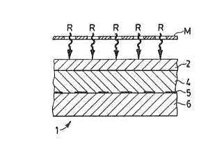
FIG. 1 is a cross-sectional ~iew of a substrate
with metal patterns, coated with layers of photoresist
being exposed to radiation through a mask.
- 6 ~ 1 7 .~
FIG. 2 is a cross-sectional view o the article
of FIG. 1 after development.
G. 3 is a cross-sectional view of the
developed article of FIG. 2 after opacification.
FIG. ~ is a cross-sectional view of the article
of FIG. 3 after a second e~posure and development.
FIG. 5 is a cross-sectional view of the artiele
of FIG. 4 after deposition of conductive material upon
the substrate.
FIG. 6 is a cross-sectional view of the article
of FIG. 5 after the remaining photoresist has been
removed.
~ETAILED D~S~RIPTIO~ QE THF, ~WI~
FIG. 1 ~s a cross-sectional view of an
integrated circuit substrate coated with layers of
photoresist being exposed to radiation through a mask.
Laminate 1, consisting of substrate 6, thick photoresist
20 layer 4, and thin photoresist layer 2 is formed by
seql~entially coating substrate 6 with these layers of
photoresist.
Suitable substrates for the present process
include silicon and compound III-V semiconductors known
25 in the art such as gallium arsenide. A preferred
substrate is a silicon wafer.
Substrate 6 is first coated with a patterned
layer of conductive contact pads 5. The patterning of
substrate 6 with contact pads 5 may be carried out by
30 vacuum deposition with a mask or by separate
photolithographic processes well known in the art. A
suitable process, for e~ample, is disclosed in U.S.
Patent No. 4,009,044 to Franco et al.
Contact pads 5 may comprise a bilayer composite
35 of titanium-tungsten alloy overcoated with gold. Also
suitable is chromium overcoated with gold. In these
_ 7 ~ 3 ~ 7 ~
cases, the titanium-tungsten alloy and the chromium are
used to improve the adhesion of the contact pads 5 to
substrate 6.
The pattern of contact pads 5 must adhere
5 generally to the predetermined pattern. That is, the
locations of contact pads 5 must coincide with the
locations where conductive material will be deposited to
form bumps 10 as shown in FIG. 5. Contact pads 5 may be
slightly larger than the impressions in thick
10 photoresist layer 4 as shown in FIG. 4, but may not
touch as that would render the resulting product of the
process useless as an integrated circuit component.
Thick photoresist layer 4 may be coated on
substrate 6 by any suitable photoresist coating method
15 such as spin coating. Thick photoresist layer 4
preferably is a "positive working" photoresist (i.e., a
material whose solubility increases when exposed to
activating radiation). A negative working photoresist
(i.e., one that becomes less soluble when exposed to
20 activating radiation) is undesirable as thick
photoresist layer 9 due to the difficulty of removing
negative working, exposed thick photoresist 4 from
substrate 6 after bump formation.
Positive working photoresists suitable as thick
25 photoresist layer 4 include sensitized
phenol-formaldehyde resins (also known as ~novolak~
resins), sensitized cresol-formaldehyde resins, and
sensitized polysulfonamide resins. Preferred positive
working photoresists for thick photoresist layer 4 are
30 novolak-based resists having a viscosity ranging from
100-10,000 centipoise at 20 degrees Celsius, such as
AZ-4620, supplied by American Hoechst Corp.
The thickness of thick photoresist layer 4 is
largely dependent on the coatability and developability
35 of the resist, the size requirements of bumps 10 to be
ultimately formed on substrate 6 and the desired packing
~ 3'~
density of bumps, (number of bumps/unit area). Suitable
thicknesses of layer 4 are in the range of 5-50 ~m,
preferably 30 ~m.
Thin photoresist layer 2 is spin coated over
5 thick layer 9. Thin layer 2 may be a positive or
negative working photoresist. Suitable positive working
photoresists include sensitized phenol-formaldehyde
resins, sensitized cresol-formaldehyde resins, and
sensitized polysulfonamide resins. Preferred positive
10 working photoresists for thin layer 2 are novolak-based
resists having a viscosity ranging from 1 to 50
centipoise at 20 degrees Celsius.
In a preferred embodiment of the present
process, thin photoresist layer 2 is a negative working
15 photoresist. FIGS. 1-6 are directed to this
embodiment. The combination of thin negative working
photoresist 2 and thick positive working photoresist 9,
as shown in laminate 1 of FIG. 1, results in
photoresists with different propensities for accepting
20 opacifying agents. This permits use of a large
select;on of opacifying agents which will be readily
accepted by thin photoresist layer 2 and not accepted by
thick photoresist layer 4.
Preferred negative working photoresists are
25 those resists that show minimal intermixing with the
underlying resist layer, such as those disclosed by U.S.
Patent No. 4,808,510 to Snow, U.S. Patent No. 4,355,087
to Martin, and U.S. Patent No. ~,315,978 to Hartman,
which are llereby incorporated by reference.
Thin photoresist layer 2 must be thick enough
to mask thick photoresist layer ~ from subsequent
e~posure, once opacified. Suitable thicknesses of thin
photoresist layer 2 are in the range of 0.2 to 2.0 ~m,
preferably 1.0 ~m.
- 9 ~2~
FIG. 2 is a cross-sectional view of the article
of FIG. 1 after development. Laminate 1 is exposed
through mask M to radiation R of a wavelength to which
thin photoresist layer 2 is sensitive. Preferably,
5 exposure in FIG. 1 is carried Ollt by conventional
projection printing -- i.e. e~posure through a mask that
does not contact laminate 1. Tllin layer 2 may be
exposed with a variety of sources including electron
beam, ion beam, ~-rays, deep ultraviolet, ultraviolet,
10 or visible radiation. Radiation of a wavelength between
300 to 500 nm is preferred and between 365-436 nm is
most preferred.
As shown in FIG. 2, laminate 1 has been
developed after e~posure by immersion in developer
15 solution to remove the unexposed portions of thin
photoresist layer 2 to form the negative of the
predetermined pattern of mask M. Preferred developers
include water-based or alcohol-based developers. The
laminate of FIG. 2 consists of substrate 6, thick
20 photoresist layer 4 and patterned, thin photoresist
layer 2.
Ne~t, the remnants of thin photoresist layer 2
in FIG. 2 are treated with an opacifying agent to
convert this remainder of layer 2 to conformal optical
25 mask 3, as shown in FIG. 3. Opacification may be
carried out by a process such as solution imbibition,
vapor imbibition, or selective deposition. The
opacifying agent must absorb the radiation which will be
subsequently used to e~pose the laminate. Suitable
30 opacifying agents include dyes, pigments, and compounds
containing elements whose atomic number is greater than
25, such as lead. Preferred are W, near-W , and
visible light absorbing dyes such as those disclosed in
U.S. Patent No. 4,876,167 to Snow.
FIG. 3 is a cross-sectional view of the
developed article of FIG. 2 after opacification. FIG. 3
.
.
shows a laminate consisting of substrate 6, thick
photoresist layer 4 and conformal optical mask 3. The
laminate of FIG. 3 is exposed to activating radiation
which both activates thiclc, positive working photoresist
5 layer 4 and is absorbed by conformal optical mask 3.
Thick layer 4 may be e~posed with electron beam, ion
beam, ~-rays, deep-ultraviolet, ultraviolet, or visible
radiation. The radiation may be the same wavelength as
that used to e~pose thin photoresist layer 2 in FIG. 1
10 or may be different. Preferred is radiation with a
wavelength of 300 to 500 nm. Wavelengths of 365-436 nm
are most preferred.
Ne~t, the laminate of FIG. 3 is developed to
remove the e~posed, unmasked photoresist in thick
15 photoresist layer 4. Such removal can be achieYed by
dissolving the photoresist in an appropriate developer.
Suitable developers include the known alkaline, positive
photoresist developers containing t~tramethylammonium
hydro~ide. Such developing produces the laminate of
20 FIG. 4, which is a cross-sectional view of the article
of FIG. 3 after a second exposure and development. This
article consists of substrate 6, patterned thick
photoresist layer 4, and conformal mask 3.
FIGS. 5 and 6 illustrate the use of the
~5 laminate of FIG. 4 for wafer bumping in the production
of integrated circuits. FIG. 5 is a cross-sectional
view of the article of FIG. 4 after deposition of
conductive material upon the substrate. The laminate of
FIG. 4 is used as a template for the deposition of bumps
30 10 on substrate 6. As shown in FIG. 5, bumps 10 are
deposited in the patterned openings created in thick
photoresist layer q by a process such as
electroplating. Bumps 10 may be any highly conductive
material, such as gold, silver, nickel or copper.
Finally, remaining thick photoresist layer 9
also is removed by dissolution in a solvent, such as
fi ~
acetone or l-methyl-~-pyrrolidinone. Thick photore~ist
layer 4 may also be removed by dry etching processes.
Conformal mask 3 is either dissolved by the solvent used
to remove photoresist layer 4 or is simply lifted off by
5 solvent action or removed by dry etchirg. FIG. 6 is a
cross-sectional view of the article of FIG. 5 after the
remaining photoresist has been removed.
The process of the present invention produces
an excellent reproduction of the original mask pattern
10 that e~hibits a high degree of pattern fidelity. It is
very suitable as a template for the deposition o~
bonding pads as illustrated in FIGS. 5-6. The precise
pattern reproduction allows a ma~imum number of bumps to
be placed on the chip, which results in a high lead
15 count. Therefore, this process is very useful in VLSI
technology.
The following e~ample is illustrative.
~ ' ' ` , .
.
~XA~ }
Silicon wafers four inches in cliameter were
5 used as the substrate for the photopatterning
experiments. First, a 30 ~Im thick film of high
viscosity, novolak-based, positive working AZ4620
photoresist ~which is supplied by American Hoechst
Corp.) was spun on wafers coatedl with a
10 titanium-tungsten alloy and golcl. The thick photoresist
was spun on using a double coat process and baked twice
for 40 seconds at 125C. Then, a solution of 15 g
poly(vinylbenzyl chloride) quaternized with
N,N-dimethylethylamin~ cinnamate and
15 3-dimethylamino-1-propanol and 0.625 g of a 1:1 weight
ratio mixture of pyridinium
3-~(7-methoxy-2-ogo-2H-l-benzopyran-3-yl)
carbonyl]-l-methyl salt and 4-methylbenzenesulfonic acid
sensitizer and 0.25 g of nonylpheno~ypolyglycerol lOG
20 surfactant (supplied by Olin Corp.) dissolved in 88 9 of
water was applied to nonrotating wafers which were then
spun for 5 seconds at 500 revolutions per minute (rpm)
and for 55 seconds at 2000 rpm. The coated wafers were
air dried in a clean hood for 17 hours at room
25 temperature. The thickness of the thin photoresist
layer at this point was ~1 ~m.
The process involves imagewise light e~posure,
development, and dye imbibition of the thin photoresist
layer. This is followed by flood e~posure and
30 development of the thick photoresist layer.
The negative-working thin photoresist layer was
exposed, using a hi~h-pressure mercury vapor light
source by contacting the wafer face-to-face with the
half-tone screen negative. The optimum e~posure found
35 necessary to produce a useful dot pattern was 5 seconds
at 17 milliwatts per square centimeter power density.
- 13 -
7.~
Washout processing using spray development was
carried out over a period of ~0 seconds using pH-4
phthalate buffer solution.
The dye imbibition process was carried out for
5 4 minutes using the solution of 0.75 g of
3-cyano-1-phenyl-4-[3-(carboxymethylaminosulfonyl)phenyla
~o]-2-pyrazolin-5-one UV-blue absorbing yellow dye and
0.3 9 nonylphenoxypolyglycerol lOG surfactant ~supplied
by Olin Corp.) dissolved in 100 ml of pH-10 borate
10 buffer system. The wafer was spray-rinsed for 5 seconds
using fresh pH-10 borate buffer solution and air dried
for 30 minutes at room temperal:ure.
The thick, positive-working resist layer was
flood e~posed using the dyed, patterned, thin
15 photoresist layer as the conformal optical mask.
E~posure was carried out using a high-pressure mercury
vapor light source spectrum filtered through Wratten 2B
and 34A filters. In the plane of the wafer, the
intensity was 2.5 milliwatts per square centimeter. The
20 optimum exposure time found necessary to produce a
useful pattern ranged between 15 and 30 minutes.
The exposed thick photoresist layer was
spray-developed while spinning at 350 rpm for 5 minutes
- using tetraethylammonium hydro~ide-based AZ400K
25 developer (supplied by American Hoechst Corp.), diluted
with water in the ratio of 1 part developer to 3 parts
distilled water, spray-rinsed for 3 minutes using
distilled water, and air dried at room temperature.
The two-dimensional pattern defined in the
30 thick photoresist layer produced an e~cellent
reproduction of the original half-tone screen mask
pattern.
Although the invention has been described in
detail, for the purpose of illustration, it is
35 understood that such detail is for that purpose and
variations can be made therein by those skilled in the
.
- .
.
1~- 2~ 7~
art without departing from the spirit and scope of the
invention which is defined by the following claims.
: . .
. . ,, ,.. ~ : :
:
:
~. ~ .. .