Note: Descriptions are shown in the official language in which they were submitted.
~0~2546
MICROWAVE TRANSCEIVER USING THE TECHNIQUE
OF MULTILAYER PRINTED CIRCUITS
BACKGROUND OF THE INVENTION
The present invention relates to microwave
transceivers and, more particularly, to those using the
technique of printed circuits for their
transmission/reception and microwave filtering unit and
for their modulation-demodulation unit. The making of
these two units should take account of the fact that
the transmission/reception and the filtering are done
at a frequency of some gigahertz while the working
frequency of the modulator/demodulator is considerably
lower: of the order of 100 kHz.
Given its working frequency, the
transmission/reception unit should be entirely shielded
and not only should the transmission-reception be
electromagnetically insulated from the filtering but
also the circuits corresponding to the different
functions relating to the transmission-reception should
be strictly insulated from one another.
There are known transceivers working in microwave
mode wherein, for transmission-reception, each function
is carried out on an individual printed circuit. The
different printed circuits are embedded in the housings
of a metal piece carved from the block or obtained by
molding and then machining. One or more Lids are
screwed on to the metal piece to close the housings.
~o~~~~~
2
The microwave filter, which is of the type with
resonator, is enclosed in a chamber that is formed
by two half-shells fixed to the metal piece which
contains the transmission-reception unit. The
modulation-demodulation unit is mounted on a printed
circuit that is proper to it. The internal connections
of the transmission-reception and filtering unit are
made by holes drilled in the partitions. The
connections between the transmission-reception and
filtering unit and the rest of the transmitter,
including the modulation-demodulation unit, are made by
using bypass circuits.
These known embodiments of microwave transceivers
have certain drawbacks: owing to the number of parts to ,
be assembled, the operations of mounting and
dismantling the devices are lengthy, and there are
substantial risks of microwave leakage. Furthermore,
the making of the connections between the different
printed circuits is a very delicate task.
i gUrIMARY OF THE INVENTION
The present invention is aimed at circumventing or
at least at reducing these drawbacks.
This is obtained by the use of a single printed
circuit to mount both the transmission-reception and
filtering unit and the modulation-demodulation unit.
Furthermore, all the connections relating to these two
units can be made in the printed circuit, at least up
to a connector with several contacts that is fixedly
2062546
joined to the printed circuit, when the connection also
relates to a unit other than the two above-mentioned
units
According to the present invention, there is
provided a microwave transceiver comprising a first
unit relating to the modulation-demodulation, a second
unit with first microwave circuits relating to the
transmission-reception functions and a second microwave
circuit relating to the microwave filtering function, a
multilayer printed circuit with a first face on which
there is mounted the first unit, with an internal layer
constituted, at least partially, by a conductive plate,
with a second face having conductive tracks that form
an irregular conductive grid defining compartments, and
conductive connections within the compartments, and
with metallized holes, also known as via holes, that
form lines of dots in the tracks and are located at
distances from one another that are notably smaller
than the working wavelengths of the transceiver, a
thick conductive lattice having walls that lie on the
tracks and cover them entirely, and a conductive lid
that covers the lattice, wherein the microwave circuits
are positioned in the compartments with a one-to-one
relationship between the compartments and the functions
and wherein the tracks, the lattice, the metallized
holes and, at least for the transmission-reception
functions, the plate and the lid form casings which
4
206256
determine electromagnetic protection volumes and which
enclose the microwave circuits.
BRIEF DESCRIPTION OF THE DRAWTNGS
The present invention shall be understood more
clearly and other characteristics shall appear from the
following description and from the figures pertaining
thereto. Of these figures:
- Figures 1 and 2 show sectional views of parts of
transceivers according to the invention;
- Figure 3 shows a view in perspective of elements
that go into the making of a transceiver according to
the invention.
In these figures, the corresponding elements are
designated by the same references.
MORE DETAILED DESCRIPTION
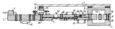
Figure 1 shows a multilayer printed circuit 1 on
which there are mounted different components as well
as, on its upper face, a thick, conductive, metal
lattice 2 closed by a metal lid 3 associated with an
electromagnetic seal 23. A metal half-shell 4 is
mounted on the lower face of the circuit 1.
Figure 3 shows a view, in perspective and before
assembly, of 'the manner of making a multilayer printed
circuit 1, a thick conductive lattice 2 and a
conductive lid 3 designed for a transceiver according
to the invention which, as it happens, is not that of
figure 1 or even that of figure 2; this makes it
206546
possible to see a greater number of embodiments and to
note their common characteristics, namely:
- a printed circuit, of which the upper layer,
which will be called a support layer, has an
irregular grid 10 formed by wide conductive tracks
with conductive links such as 11 within
compartments defined by this grid: it must be
noted that, to simplify the drawing, the
metallized holes such as the holes 20 and 40 of
ffigures 1 and 2 haue not been shown in figure 3
where they would have been shown as a line of dots
positioned substantially in the middle of the
conductive tracks of the grid 10,
- a conductive lattice 2 which reproduces the
pattern of the grid 10 in thickness and is
designed to be soldered to this grid,
- a lid 3 with the external dimensions of the
lattice on which it is mounted by means of a set
of screws (not shown) that go through the lid to
penetrate threaded holes drilled in the lattice,
In a standard way, the assembly further includes a
flexible electromagnetic seal (not shown) which
itself also reproduces the pattern of the grid 10
and is designed to be mounted between the lattice
and the lid; a seal such as this is shown in
figures 1 and 2 where it bears the reference 23
and where, to clearly distinguish the lid 3 from
the seal 23 and from the lattice 2, these three
206240
6
elements have been slightly moved away from one
another whereas, after mounting by means of
screws, they are perfectly joined to one another.
A part of the lattice 2 according to figure 1,
constitutes a half-shell 24 and the two half-shells 4
and 24 are positioned so as to constitute a shell. The
interior of this shell encloses a microwave filter,
only one stub 44 of which is seen in figure 1. The
edges of the two half-shells are connected by
metallized holes such as 40, evenly arranged at about 5
mm from one another. Given a working frequency of 4,3
GHz for the filter which encloses the shell, these
metallized holes are at a distance from one another
that is smaller than one-twentieth of the working
wavelength in the substrate of the printed circuit 1;
these holes therefore form a screen to the microwaves
created within the shell by the filter.
Other metallized holes such as 20, also planed
away from one another at distances of about 5 mm, form
the connection between the other parts of the lattice,
which lie on the printed circuit 1, and a conductive
plate 5. The plate 5 constitutes a partial internal
layer of the printed circuit 1. It is placed directly
in front of the lattice 2, except inside the shell
where it is absent. Thus, the lattice 2, the lid 3, the
metallized holes such as 20 and the plate 5 determine
volumes that are electromagnetically protected, as is
the interior of the shell 24-4. Within these protected
262546
volumes, there are mounted the electronic circuits
corresponding to the different functions of the
transmission-reception part proper of the transceiver
considered.
The electromagnetic protection elements that thus
surround the transmission-reception part and the
microwave filtering constitute, for the external
environment, a screen against the microwave
disturbances produced by the circuits located within
volumes that they demarcate. This enables the
modulation-demodu7.ation part of the transceiver to be
mounted on the lower face of the multilayer printed
circuit, where this face is not covered by the
half-shell 4.
Figure 1 shows a certain number of components
mounted on the printed circuit: a surface-mounted
component 51 and a component 52 with special mounting
in the microwave part; a surface-mounted component 61
and a standard component 62 in the
transmission-reception part. The connections between
the microwave part and the modulation-demodulation part
are done by metallized holes such as 60 or metallized
holes associated with bypass circuits such as 'the
circuit 53.
The links with the rest of the transceiver are
provided by an ordinary multicontact connector 7
soldered to the printed circuit.
20fi2~46
In order to facilitate the connecting of the
lattice to the printed circuit 1 and to strengthen this
connection mechanically, the lattice has pins, such as
41, which are embedded in certain of the metallized
holes, such as 40, of the grid 10.
Furthermore, it must be noted that those layers of
the printed circuit 1 which are located on the
microwave part side have been made of
polytetrafluoroethylene laminate, in view of the high
performance characteristics of this material in
microwave applications, while the other layers have
been made of epoxy resin laminate in view of the
attractive price of this widely available laminate.
Figure 2 corresponds to an alternative embodiment
of the transceiver of figure 1, in which the filtering
part alone is different. The half-shell 4 has been
eliminated and replaced by a conductive layer in the
printed circuit. Besides, this Layer is only the layer
according to figure 1 but is more extensive so as to
be in front of the microwave ffilter. In this variant,
the upper half-shell 24 is closed by the lid 3 while,
in the embodiment according to figure 1, the half-shell
24 was a single piece, the lid 3 therefore having no
role of electromagnetic protection with respect to the
microwave filter. It should be furthermore noted that,
in the embodiment according to figure 2, the stub 44 is
thinner than in the embodiment according to figure 1
because it cannot take the entire thickness of the
262546
circuit. This is why, in order to keep the same working
frequency, the volume of the cavity which has already
been reduced by the elimination of the lower half-shell
is further reduced by a protuberance 34 from the lid 3,
this protuberance being thicker than the bottom,
parallel to the printed circuit 1, of the half-shell 24
according to figure 1.
The present invention is not limited to the
examples described. It is thus that the metal lattice
may be constituted by several meshes joined together,
for example, by soldering.
In the same way, the technology of printed
circuits, with its metallized holes, enables the
insertion of a sandwiched heat sink: a metal plate may
be positioned within the stack of the layers of the
printed circuit, and this plate may be constituted by
the plate 5, provided that it is given sufficient
thickness far the desired calorie-discharging effect.