Note: Descriptions are shown in the official language in which they were submitted.
2062776
- 1 -
DIGITAL AUTOMATIC GAIN CONTROL
THE FIELD OF INVENTION
This invention is concerned with digital automatic gain control. More
particularly, this invention is concerned with Automatic Gain Control
(AGC) for discontinuous signals in a receiver having limited dynamic
range.
BACKGROUND OF THE INVENTION
Although the concept of Automatic Gain Control (AGC) in radio signal
reception is well understood, automatic gain control of Time Division
25 multiplexed Multiple Access (TDMA) signals presents new challenges to
the land-mobile industry.
In wideband TDMA systems, such as the cellular system proposed for
use in Europe, an RF channel is shared (time-division-multiplexed)
30 among numerous subscribers attempting to ~ccess the radio system in
certain ones of various time-division-multiplexed time slots. The time
slots are arranged into periodically repeating frames. Thus, a radio
communication of interest may be periodically discontinuous --
interleaved with unrelated signals trans",illed in other time slots. The
35 unrelated signals (of widely varying strength) must not influence the gain
-CE00332R -1 -
,,
:, .
WO 91/17606 - PCI/US91~02409
-2- 206277S
control of the signals of interest. A formidable challenge then is to
provide Automatic Gain Control of these periodically discontinuous
TDMA signals.
5 The challenge is further enhanced by attempting to provide digital AGC
in inexpensive receivers -- those having limited dynamic range. Since
these signals may vary by as much as 100dB in the land-mobile
environment, but ~ est 8-bit Analog-to-Digital converters (A/D) for
digital signal processing are limited to 48dB dynamic range, techniques
10 must be developed for controlling the gain of the signal to keep it within
the limited dynamic range of the recGivor. The challenge then is to
handle a 100dB discontinuous signal with a 48dB device; otherwise,
prohibitively expensive AtDs with greater dynamic range must be utilized.
15 Another challenge for gain control is introduced by the digital nature of
these TDMA trans",ission systems. G~USSj~rl Minimum Shift Keying
(GMSK) modulates the quadrature phases ot the signal such that the
power of the received signal is more difficult to measure, and neither of
the quadrature phases, taken alone, is proportional to the received signal
20 power.
This invention takes as its object to overcome these challenges and
realize certain advantages, presented below.
SUMMARY OF THE INVENTION
In accordance with the preferred embodiment of the invention, there is
provided a mechanism for Automatic Gain Control in a receiver. It
comprises. determining, within a certain dynamic range, the difference in
30 power between the desired signal and a signal received, and providing
open loop gain control for the signal in response to the differential so
determined, scaled by the receiver's gain characteristics, such that the
signal is positioned within dynamic range so as to reduce saturation and
noise.
NO 91/17606 PCI /US91/0~409
-3- 206277~
In accordance with one embodiment of the invention, there is provided a
method of digital Automatic Gain Control (AGC) in a receiver having
limited dynamic range, particularly for discontinuous signals. The
method comprises detecting the level of a received and AGC'd
5 discontinuous signal, comparing the level of the AGC'd signal relative to
the dynamic range of the receiver, and adjusting the AGC to est~blish a
desired rel~ionship between the AGC'd signal and the dynamic range
li",i~alion. There is also provided a method of handoff in a TDMA
cellul~r-type trans",ission system utilizing this method of AGC control.
The method for Automatic Gain Control (AGC) of discontinuous signals in
a receiver having limited dynamic range is further characterized by:
digitizing a received and AGC'd discontinuous signal and converting the
digitized samples to a power sample to sense the power of and detect
15 the level of the signal, comparing the level of the AGC'd signal relative to
the dynamic range of the receiver; and coarsely-adjusting by either
progressivaly attenuating the signal until it falls within the dynamic range
of the receiver or by progr~ssively gain-amplifying the signal until it falls
within the limited dynamic range of the receiver and finely-adjustin~ the
20 AGC of the received signal until optimum use of the full (albeit limited)
dynamic range of the signal pl~cessing stages is about 6-12 dB below
the maximum to esl-~blish a desired relationship between the AGC'd
signal and the dynamic range limitation.
BRIEF DESCRIPTION OF THE DRAWINGS
Additional objects, features, and advantages of the invention will be more
clearly understood and the best mode contemplated for practicing it in its
preferred embodiment will be appreciated (by way of unrestricted
30 example) from the following detailed description, taken together with the
accompanying drawings in which:
Figure 1 is a simplified block diagram of the invention.
WO 91/17606 PCr/US91/02409
4 206:277~6
Figure 2 is a functional block diagram of the preferred embodiment of the
invention.
Figure 3 is a diagram ot the AGC control process according to the
5 invention.
Figure 4 is a simplified diagram of an altemate embodiment of the
Invention.
10 Figure 5 is a diagram of a preferred ~",bGdiment of the AGC control
process according to the invention.
Figure 6 il!ustrates five overlapping regions of the useful A/D range
(3~dB) spanning the expected signal range of -20dB to -1 1 OdB.
DETAILED DESCRIPTION
Figure 1 is a simplified block diagram of the invention; it illustrates gain
20 control in a digital quadrature receivGr. It illustrates, in series, an RF
receiver section (IF), a quadrature de",~ or (I/Q) having In-phase and
Ouadrature phases, Analo~-to-Digital converters (A/D), a Digital Signal
P,ocessor (DSP), and a Digital-to-Analog converter (D/A) providing
Automatic Gain Control (AGC) to the receiver section (RF/IF).
In operation, the signal is received, converted to an intermediate
frequency and gain amplified in the receiver section (RF/IF); quadrature
demodulated (I/Q) into In-phase and Quadrature components; digitized in
Analog-to-Digital converters of limited dynamic range (A/D); and
30 converted to a power sample in the Digital Signal Processors (DSP) to
detect the level of the signal. In the Digital Signal Processors (DSP), the
signal level is compared relative to the dynamic range of the receiver,
and the AGC is e~ljusted in the Digital-to-Analog converter (D/A) to
WO 91/17606 - PCI/US91/02409
5 2062776
eslshlish a desired relationship between the AGC'd signal and the
dynamic range limitation of the receiver.
More concrvtely, the power level ot the AGC'd si~nal is compared
relative to a desired power level in the stage having the dynamic range
limitation.
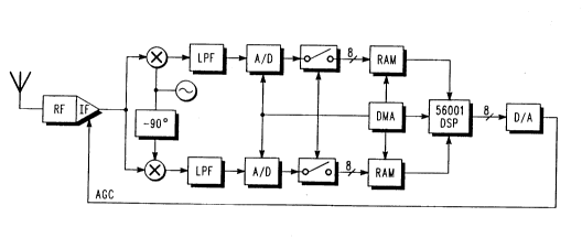
Figure 2 is a functional block diagram of the preferred embodiment of the
invention. Figure 2 illusl,dtes, in line, an RF receivar s~tion (RF!IF); a
quadrature demo~ul~tor (I/Q) having In-phase (I) and Quadrature (Q)
phase mixers whose outputs are Low Pass Filtered (LPF); and, under
Direct Memory Access cohtrol (DMA), 8-bit Analog-to-Digital converters
(A/D), tri-state gates, Random Access Memories (RAM), and a 56001
Digital Signal Processor (56001 DSP); and a latching Digital-to-Analog
converter (D/A) providing Automatic Gain Control (AGC) to the receiver
section (IF). This GMSK receiver is comprised of a conventional RF
stage, mixing and filtering that feeds a 10.7 MHz IF signal to a
conventional AGC-type IF amplifier (IF), such as a Motorola MC1350.
The IF amplifier feeds a conventional l/Q demodulator comprised of a
10.7 MHz loca os~ 0r, a 90 degree phase shifter, a pair of mixers and
a pair of low pass filters (LPF). The 8-bit flash A/Ds, such as RCA
CA3318CE's, provide 48dB of dynamic range and are, in large part,
responsible for the dynamic range limitation of the receiver. A Motorola
56001 Digital Signal Processor (56001 DSP) is used for signal
~c~uisition, signal level detection, and AGC control. The 56001 DSP is
supported by conventional clock and timing circuitry (not shown) and
ROMs for programmed control (not shown). An Analog Devices 7528LN
is suitable as the latching Digital-to-Analog converter (D/A) that provides
Automatic Gain Control (AGC) to the receiver section (IF).
The receiver operates in a TDMA system having 8 time slots in each 4.8
millisecond frame; 135 kilobits/second are transmitted in each
quadrature phase. In operation, for each time slot, a retained previous
AGC setting is fetched (DMA) from memory (RAM) through the Digital
WO 91/17606 PCr/US91/02409
-6- 2062776~-~
:
Signal Plocessor (56001 DSP) and applied to the Digital-to-Analog
converter (DtA), providing Automatic Gain Control (AGC) to the receiver
section (RF/IF). The received signal, after being gain-controlled and
quadrature~le",~Ju~tsd is digitized by the Analog-to-Digital converters
5 (AID) to provide multiple pairs ot samples per bit interval, which are
stored in memory (RAM) under Direct Memory Access control (DMA) of
the tri-state gates. The samples are retrieved from memory (RAM) and
converted in the 56001 DSP to a power sample by summing N pairs (32
to 128 pairs in the prefer.~ e.,l~liment) to obtain a O value and an I
10 value, and taking the square root of the sum of the squares of the O and I
values. The square root is proportional to the average power of the
received signal (an instantaneous power sample from a single pair
cannot be reliably obtained due to the variability in the received signal
slrer,~h). A preferred altemative measure for the power sample may be
15 obtained by simply summing the squares of the Q and I values.
Again, more concretely, the power level of the AGC'd signal is compared
relative to a desired power level in the stage having the dynamic range
limitation. Thus, to prevent short-term saturation of the 8-bit Analog-to-
20 Digital converters (A/D), the AGC wants to est~blish and maintain thelevel of the AGC'd signal at a nominal level of about 6-1 2dB (9dB in the
preferred embodiment) below the maximum output of the AID.
Figure 3 is a diagram of the AGC control process according to the
25 invention.
The basic control pr~ cess is to:
detect the level of a received and AGC'd discontinuous signal,
compare the level of the AGC'd signal relative to the dynamic
range of the receiver, and
adjust the AGC to establish a desired relationship between the
AGC'd signal and the dynamic range limitation.
WO 91/176~K PCI /US91/02409
-7- 2062776
-
The average power, as measured above, is then subtracted from a power
level representative of the desired nominal level (or 9dB, hereinaner
given as Odb reference) to ~'u)~te the power error. This r--lc~ted
5 power error is further tactored by an adjustment that compensates for the
overall loop gain cha,acle,islios, resulting in an AGC Error (AGCE). If the
AGC Error (AGCE) is within the margin below full output (9dB), then the
prevailing AGC setting (Filtered AGC Number- FAGCN) is finely-
adjusted by the amount of the Error (AGCE). If the Error is greater than
10 the margin (9dB) but inside the dynamic range of the A/D (48dB - 9dB =
39dB), then adjust by the amount of the Error (AGCE) plus slightly more
than the margin (9dB + 1dB = 1 OdB). If the Error falls below the dynamic
range of the A/D, then coarsely-adjust by the amount ot the dynamic
range (48dB); if the Error is above the dynamic range, then adjust by
15 slightly more than the margin (9dB + 1dB = 1OdB). Finally, the current
Error ~-'aJ'~tion and the previous gain setting (FAGCN) become the
inputs to a digitally recursive infinite impulse response low pass filter
(which is well ul,de.stood by those ordinarily skilled in the art) to derive a
new Filtered AGC Number (FAGCN). Thus, the signal is pro~ressively
20 gain-amplified (or gain-attenuated) until the signal falls within the
dynamic range of the A/Ds and is further amplified (or attenuated) until
optimum use (with appropriate margin) of the full (albeit limited) dynamic
ran~e of the A/Ds is obtained. The result of these various approximations
for a plurality of TDM time slots may then be retained in memory (RAM)
25 for resuming AGC control when the respective signals are expected to
resume.
Furthermore, as these various gain calculation results are representative
of the actually received signal strength (with appropriate compensation
30 for overall loop gain characteristics), these gain determinations can be
reported to the transmitting station for purposes of esteblishing
transmission gain levels that optimally utilize the dynamic range of the
receiver, thereby increasing spectral efficiency and frequency reuse in
WO 91/17606 PCI/US91/02409
-8- 20627-7~
ths system -- particulafly cellular systems. Moreover, in a cellular-type
system, the signal strength (gain determination) may be reported to the
transmitting station by the receiver and hand off the transmission when
the AGC adjustment crosses a certain threshold. Also, the signal
5 strength (AGC level) of an adjacent cell (time slot) can be determined
and evaluated to f~ e hand-off.
Figure 4 is a simplified- diagram of an altemate embodiment of the
invention. It illuslrales an analog implementalion of Auto".atic Gain
10 Control that utilizes a power averaging circuit and comparator to
implemsnt the control pr~cess of Figure 3, describQd above. The power
averaging circuit is well known by those ordinarily skilled in the relevant
art and can readily be adapt~ to conform to the control process
described above.
In summary then, there has been provided a ",ethGcJ of digital Automatic
Gain Control (AGC) in a r~ceiver having limited dynamic range,
particularly for discontinuous signals. The method comprises detecting
the level of a received and AGC'd discontinuous signal, comparing the
20 level of the AGC'd signal relative to the dynamic range of the receiver,
and adjusting the AGC to est~hlish a desired relationship between the
AGC'd signal and the dynamic range limitation. There has also been
provided a -,etl.G~I of handoff in a TDMA cellu~r-type trans",;ssion
system utilizing this ",ethoJ of AGC control.
The method for Automatic Gain Control (AGC) of discontinuous signals in
a receiver having limited dynamic range has further been characterized
by: digitizing a received and AGC'd discontinuous signal and converting
the digitized samples to a power sample to sense the power of and
30 detect the level of the signal, comparing the level of the AGC'd signal
relative to the dynamic range of the receiver; and coarsely-adjusting by
either progreæively attenuating the signal until it falls within the dynamic
range of the receiver or by p~o~ressively gain-amplifying the signal until it
falls within the limited dynamic range of the receiver and finely-adjusting
VO 91/17606 PCI`~US91/02409
9 ~062776
the AGC of the received signal until optimum use of the fuli (albeit limited)
dynamic range of the signal processing stages is about 6-12 dB below
maximum sensitivity to establish a desired relationship between the
AGC'd signal and the dynamic range limitation.
This ~iscu~sion pres~lpposed that the A/Ds provide the most severe
constr~int on the dynamic range of the rec 3iv0r; however, this invention
is 6qu^~y ~pli~l~ without regard to the particular stage providin~ the
most severe constraint on the dynamic range of the receiver.
10 Accordingly, all d;scussiQn has been framed in terms of the limited
dynamic range of the receiver.
Figure 5 is a diagram of a preferred embodiment of the AGC control
p,ocess ac~o~ding to the invention. It illustrates the control process for
15 an open loop improvement to the digital AGC presented thus far. The
foregoing e,nb~Ji",ent iteratively settled on the proper AGC through
- progressive, closed loop control. This preferred embodiment utilizes a
lookup table (incG"~r~ting all the receiver characteristics and non-
linearities, including the A/D non-linearities) with the calculated
20 difference in power bet,~Gen that desired to obtain maximum utilization of
the A/D dynamic range and the current actual power received at the A/Ds
as an index into the table to obtain the next AGC setting required to settle
at the desired power level.
25 The table is derived in a laboratory setting where the AGC (power) level
is est~lished at the desired level while the power generated from a
signal generator couplQd to the antenna input nece~ry to esla~lish
certain power differentials at the A/Ds is noted. In this fashion, the AGC
level required for any given power differential can be extrarol~ted.
All of the signal processing of Figure 5 takes place in the digital signal
- pro~essor (DSP) of Figures 1 & 2. Returning to Figure 5, the power
seen at the AtDs is or~oul~ted (501 ) as the sum over sixty-four samples of
the squares of the demodulated (I/Q) signal samples. The difference in
WO 91/17606 PCr/US91/02409
-10- 2062776
power (~dB) between that seen at the A/Ds (PA/D) and that desired (Pd)
is determined (502). The power (PdBm) during the timeslot is
dete.",inad (503) from the currect D/A setting and the power differential
(~dB) and then indexing into the lookup table with the to find the power
5 for that timeslot. As has been "enlioiled the lookup table is a function of
the ~ceivers gain control ch~r cteri~tics. This PdBm setting from many
timeslots (cG.,.p,ising the discon~inuous communication) is averaged in
an FIR filter (504) ! form a better power estimate of the faded signal that
is reported to the ~ns,ni~l~r for hando~ .Jete.",inal;ons (506).
The power differential (~dB) itself is also averaged over several timeslots
(since the AGC cannot track through signal fades) in an FIR filter (505) to
dete.",ine the avera~e power difference (AVG~dB) from the desired (Pd)
to determine when AGC settling has occurred (507). lf this short-term
1 5 average error (AvGadB) is not greater than, say half-scale (6dB) off of
- A/D saturation (508) and not less than (510) the noise quantization level
(-30dB) then an IIR filter, or~leaky i,~e~ralor,~ (513) determines the
speed of the AGC response to correct the present D/A setting by table
lookup (512). This u~l~'e J D/A value is then stored (514) for use with
subse~uent ti",eslQts.
In those few instances where the signal s power is not within the A/Ds
(useful) range - i.e. the average power differential is not within the
usable (+6dB through -30dB) dynamic range of the 8-bit A/Ds (48dB) --
the useful range of the A/Ds is wiriJowed up through gain reduction (509)
when the signal is clipped and the A/Ds are saturated and windowecJ
down through increaseJ gain (511) when noise quantizalion occurs and
the signal is insumciently strong (see Figure 6). The AGC gain is scaled
(and the A/Ds window adjusted) by the receivers gain control
characteristics incorporated in the lookup table (509 8 511).
Additionally the filters (505 & 513) are reinitialized to avoid avaeraging
in now irrelevant information.
"O 91/17606 PCI/US91/02409
-11- 2062776
Fi~ure 5 illustrated the AGC control process for ~racking timeslots
compfising one communication that is discontinuously transmitted. In
alternate timeslots, the receiver may, while idle, be monitofin~ up to 32
other carriers with strength varying across the entire -20dB to -11 OdB
5 range (see Figure 6). This same basic process is employed for this
~dj^cont cell monitofing. I lowev0r, to acco"""~Jate the much less
frequent peeks at the other carriers, each carfier is sampled just three
times dufing the multi-frame and the filter coefficients (504, 505 & 513)
must be adjusted for this slower AGC control (for example, the IIR filter
10 513 averages over eight samples for monitofin~, rather than the thirty-two
for tracking, so that it becomes more responsive for monitofing).
Similarly, the saturation headroom (508) is increased from the tracking
value of 6dB to 1 5dB be~use there is less certainty that the signal may
be at the previously observed power level.
In brief summary, there has been provided a mechanism for Automatic
Gain Control in a rec~iver. It compfises: determining, within a certain
dynamic range, the difference in power between the desired signal and a
signal recGi~fed, and providing open loop ~ain control for the signal in
20 response to the differential so determined, scaled by the receiver's gain
characteristics, such that the signal is positioned within dynamic range so
as to reduce saturation and noise.
While the preferred embodiment of the invention has been dascribed and
25 shown, it will be appreciated by those skilled in the art that other
vafiations and ",Gdifications of this invention may be implemented. For
example, this invention need not be limited to TDMA land-mobile
systems, but is ~da,~t.~le to AGC of di~ital and analog signals, including
AM, FM or TV signals.
These and all other vafiations and adaptations are expected to fall within
the ambit of the appended claims.