Note: Descriptions are shown in the official language in which they were submitted.
Z~?~
SPECIFICATION
TITLE OF THE INVENTION
Method of Fabricating Glass Su~strate for Disk
BACKGRO~ND OF THE INVENTION
1. Field of the Invention
The present invention relates to a method of
fabricatin~ a glass substrate for a disk.
2. Description of the Prior Art
Recently, there has been needed an optical memory
element as a high density mass memory element. The
optical memory element can be classified into a read only
memory, a write once memory and a rewritable memory
according to its working form. The optical memory element
to be used as the write once memory and rewritable memory
uses a substrate for a disk. The substrate for a disk
preliminarily comprises on a glass substrate guide tracks
for guiding optical beams for recording, reading and
erasing information to ~redetermined positions on the
optical memorY element, and track addresses for
identifyin8 track numbers. The track is divided into a
plurality of sectors. In the case where information
should be managed, sector addresses and the like are often
provided in advance. As shown in Fig. B, the depth of a
guide track portion lb is not equal to that of a sector
(or track~ address portion la, and the address portion la
is provided between the guide track portions lb. The
reason is as follows. In the case where the optical beams
are tracked by an optical differential method, it is
preferred that the depth of the guide track portion
approximates ~ ~ (8 x n~ and the depth of the address
portion approximates ~ / (4 x n) (where A is a
wavelength of light to be used and n is a refractive index
of a sub~trate). As shown in Figs. 9 to 13, there has
been proposed a technique for forming the guide track, the
sector (or track) address and the like on a glass
substrate by a contact printing method and a dry etching
method.
Referring to the technique described above, a
photomask i5 used for forming a glass substrate for a disk
by the contact printing method and the dry etching method.
The photomask has such a shape that a quantity of light
radiated onto the guide track portion and sector (or
track) address portion on a photoresist film is varied.
This technique will be summarized with reference to Figs.
9 to 13.
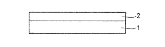
As shown in Fig. 9, a positive type photaresist film
2 is provided on a glass ~ubstrate 1, and prebaking i.
then carried out.
ir ~3 ~ ~
As shown in Fig. 10, a photomask 3 having a thin film
4 for a mask is caused to contact the photoresist f i lm 2
through the thin film 4. In this case, the thin film 4 is
not provided in a formation area Al of a sector ~or track)
address portion la. Consequently, a quantity of
transmitted light is not reduced. The thin film 4 remains
at a thickness of ahout 10 to 200 A in a formation area Bl
of a guide track portion lb. Consequently, a quantity of
transmitted light in the formation area Bl is smaller than
in the farmation area Al. Then, ultraviolet rays 5 are
radiated to expose ~he photoresist film 2 provided below
the photomask 3 (see Fig. 10). Thereafter, the photomasks
3 and 4 are removed.
As shown in Fig. 11, the photoresist film 2 thus
exposed is developed, and postbaking i5 then carried out.
Exposure is fully carried out by strong light in a
formation area A2 of the address portion la on the
photoresist film 2. Consequently, the photoresist film 2
is completely developed so that the glass substrate 1
appears. In a formation area B2 of the guide track
portion lb on the photoresist film Z, the exposure is
carried out by weaker light than in the formation area A2.
Consequently, development is stopped halfway. As a
result, the photoresist film 2 remains by a thickness
according to a quantity of tran~mitted li~ht in the
formation area Bl on the thin film 4, so that the glass
substrate 1 does not appear. The reference numeral 22a
denotes a residual photoresist film.
As shown in Fig. lZ, the glass substrate 1 is
subjected ta dry etching using gas such as CF4 or CHF3.
The photoresist film 2 shown in Fi~. 11 is also etched
simultaneously. Consequently, when etching is started~
the etching of the glass substrate 1 is advanced in the
formation area A2 so that a deep pit lla is formed on the
glass substrate 1. The residual photoresist film 22a is
etched in the formation area B2. When the glass substrate
1 appears, the etching of the glass substrate 1 is
advanced. Consequently, there is formed a groove llb
which is shallower than the pit lla in the formation area
A2. The reference numeral 22b denotes a photoresist film
which remains when the etching is completed.
As shown in Fig. 1~, the photoresist film 22b
remaining on the glass substrate 1 is removed to form on
the glass substrate 1 the address portion la as a deep pit
111 and the guide track portion lb as a shallow groove
112. Thus, there is formed a glass subetrate ll for a
disk on which the address portion la and guide track
portion lb have different depths.
The depth of the groove 112 forming the guide track
portion lb is defined by the thickness of the photoresist
film 22a remainin~ on the guide track portion lb, and the
etching speeds of the photoresist film 2 including the
residual photoresis~ film 22a and the glass substrate 1 as
shown in Fig. 11. The thickness of the photoresist film
22a is defined by a quantity of transmitted light and
developing conditions in the guide track portion lb.
Accordingly, it is difficu].t to uniformly form pits and
grooves with good reproducibility.
It is an object of the present invention to provide a
method of fabricating a glass substrate for a disk wherein
groove-shaped guide track portions and pit-shaped sector
(or track~ address portions interposed between the guide
track portions can uniformly be formed.
SUMMARY OF THE INVENTION
The present invention provides a method of
fabricating a glass substrate for a disk including guide
track portions and sector (or track) address portions of
which grooves and pits have different depths, comprising
the steps of (i) forming a photoresist film over a ~lass
substrate for an optical memory element, (ii) carrying out
exposure to define a plurality of guide track portion
formation areas and sector (or track) address portion
formation areas interposed between the guide track portion
formation areas, and carrying out development so as to
cause the glass substrate in the address portion formation
r ~ ~ ~ ~
area to appear and to cause the photoresist film in the
guide track portion formation area to remain as a first
residual film, (iii) carrying out first etching to sink
the glass substrate in the address portion formation area
by a predetermined thickness such that a pit is formed and
to remove the surface layer of the first residual film
such that a second residual film is formed, (iv) carrying
out first ashing to remove the second residual film so
that the glass substrate in the guide track portion
formation area appears, (v) carryin~ out second etching to
form a groove in the guide track portion formation area
and to further sink the pit in the address portion
formation area so that a deeper pit is formed, and (vi)
carryin~ QUt second ashin~ to remove a third residual
photoresist film which remains between the deeper pit and
the groo~e.
BRIEF DESCRIPTION OF THE DRAWINGS
Figure 1 is a view showing a first step according to
an embodiment of the present invention;
Figure 2 is a view showing a second step according to
the embodiment of the present invention;
Figure 3 is a view showing a third ~tep according to
the e~bodiment of the present invention;
Figure 4 is a view showing a fourth step according to
the embodiment of the ~resent invention;
Figure 5 is a view showing a fifth step according to
the embodiment of the present invention;
Figure 6 is a view showing a sixth step according to
the embodiment of the present invention;
Figure 7 is a view showing a seventh step according
to the embodiment of the present invention;
Figure 8 is a view showing the structure of a main
part of a glass substrate for a disk fabricated;
Figure 9 i5 a view showing a first step according to
the prior art;
Figure 10 is a view showing a second step according
to the prior art;
Figure 11 is a view showing a third step according to
the prior art;
Figure 12 is a view showing a fourth step according
to the prior art; and
Figure 13 is a view showing a fifth step according to
the prior art.
DETAILED DESCRIPTION OF THE PREFERRED EMBODIMENT
A glass substrate for a disk accordin~ to the present
invention is used as a substrate for an optical memory
element or as a substrate for a master plate for preparing
a stamper to be used for injection molding.
At first, a photoresist film 2 on a glass substrate 1
~?5~
is exposed (see Fi~. 2). Then, development is carried out
so that the surface of the glass substrate 1 appears in an
address portion formation area A2 and the photoresist film
2 remains as a first residual film 6 on the surface of the
~lass substrate 1 in a guide track portion formation area
B2 as shown in Fig. 3.
It is preferred that exposure is carried out by
radiating ultraviolet rays S onto the photoresist film 2
with the use of photomasks 3 and 4, or by a laser cutting
method using laser beams. The photomasks 3 and 4 can
completely remove the photoresist film 2 in the address
portion formation area and can stop the removal of the
photoresist film 2 halfway in the guide track portion
formation area (see Fig. 2)
The photomasks 3 and 4 are preferably comprised of a
quartz substrate 3 and a metallic pattern 4 such as
tantalum tTa), chromium (Cr) or titanium (Ti) which is
formed on the quartz substrate 3.
Referring to the laser cutting method, Ar ion laser
bea~s having a large quantity of light for exposing the
address portion formation area and Ar ion laser beams
having a small quantity of light for exposing the guide
track portion formation area are radiated onto a
photoresist plane, and scan the photoresist plane while
rotatin~ the glass substrate so that each formation area
~ A
is exposed like spirals.
The glass substrate 1 which includes the photoresist
film 2 having the first residual film 6 is subjected to
first etching. Consequently, the glass substrate 1 in an
address portion formation area A3 is sunk by a
predetermined thickness. In a guide track portion
formation area ~, the first residual film 6 is remnved to
cause a second residual film 7 to remain (see Fig. 4).
The first etching is a known method, for example, dry
etching carried out at a power of 1500 W and a pressure of
12 mTorr in a plasma at~osphere using gas such as CF4 or
CHF3.
Then, the second residual film 7 is removed by first
ashing so as to cause the surface of the glass substrate 1
to appear in a ~uide track portion formation area B4 (see
Fig. 5)-
The first ashing serves to remove an organic materialsuch as a photore~ist film. By the first ashing, the
second residual film 7 can be removed without depending on
the ununiformity of thickness distr-ibution of the first
and second residual films 6 and 7. Consequently, the
surface of the glass substrate 1 can completely appear in
the guide track portion formation area B4. More
specifically, the glass substrate 1 cannot be removed by
the first ashing. Accordingly, pits in an address portion
~~?~
formation area A4 can be defined only by the first e~ching
without depending on the selection ratio of the glass
substrate to the photoresist film (for example, 1 : 1 or 1
: 2), and the thicknesses of the first and second residual
films 6 and 7.
The first ashing is a known method, for example,
plasma etching carried out at a power of 200 W and a
pressure of 10 to 50 mTorr in an oxy~en plasma atmosphere.
Then, second etching is carried out to sink by a
predetermined thickness the glass substrate 1 which is
caused to appear by the first ashing. Consequently, there
is formed a shallow groove as a guide track portion lb in
the guide track portion formation area B4. At the same
time, the glass substrate 1 is sunk by a predetermined
thickness in the address portion formation area A3 so as
to form a deep pit as an address portion la (see Fig. 6).
The glass substrate 1 is sunk by the second etching. More
specifically, the guide track portion lb can be defined
only by the second etching without depending on the
selection ratio of the glass substrate to the photoresist
film, and the thicknesses of the first and second residual
films 6 and 7. At this time, the address portion la forms
a pit having a desired depth by the first and second
etching.
Subsequently, a third residual film 8 (see Fig. 6)
~?~'r~
provided between the address portion formation area A4 and
the guide track portion formation area B4 is removed by
second ashing. In this case, the depths of the address
portion la and guide track portion lb are not affected by
the second ashing.
According to the present invention, the depths of the
guide track portion and address portion can be defined
only by the first and second etching without depending on
the selection ratio of the glass substrate to the
photoresist film, and the thicknesses of the first and
second residual films. Consequently, the guide track
portion and address portion can have grooves and pits
uniformly formed on the glass substrate with good
reproducibility.
A method of fabricating a glass substrate for a disk
according to the present invention will be described in
detail with reference to the drawings. Figs. 1 to 7 show
fabricating steps accarding to the present invention.
As shown in Fig. 1, a positive type photoresist film
2 is provided on a ~lass substrate 1 as a glass substrate
for a disk. Then, pre'baking is carried out.
As shown in Fig. 2, a photomask 3 is caused to
contact the Photoresist film 2 through a thin film 4
for a mask. Ultraviolet rays 5 are radiated onto the
photomask 3 so as to expose the photoresist film 2. In
~?~?~f9 a~
this case, the thin film 4 is not provided in a formation
area Al of a sector (or track) address portion la.
Consequently, a quantity of light transmitted to the
photoresist film 2 is not reduced. The thin film 4
remains at a thickness of about 10 to 200 A in a formation
area Bl of a guide track portion lb. Consequently, the
quantity of light transmitted to the photoresist film 2 is
reduced.
After the photomasks 3 and 4 are removed, the exposed
photoresist film 2 i5 developed as shown in Fig. 3. Then,
postbaking is carried out. A formation area A2 of the
address portion la on the photoresist film 2 is fully
exposed by strong light. Consequen~ly, the photoresist
film 2 is completelY developed so that the glass substrate
1 appears. A formation area B2 of the guide track purtion
lb on the photoresist film 2 is exposed by weaker light
than in the formation area A2 of the address portion la.
Consequently, the development of the photoresist film 2 is
stopped halfway. The photoresist film 2 in the formation
area B2 of the ~uide track portion lb remains as a first
residual film 6. The first residual film 6 is formed at a
thickness according to a quantity of transmitted li~ht in
the formation area Bl. The above-mentioned steps are the
same as those of the prior art.
Subsequently, the glass substrate 1 includin~ the
t~
photoresist film 2 is entirely etched as shown in Fig. 4.
Consequently, the glass substrate 1 in a formation area A3
of the address portion la and the first residual film 6 in
a formation area R3 of the guide track portion lb are
simultaneously etched by a thickness of 200 to 800 A. In
this case, the first residual film 6 in the formation area
B3 is not completely removed so as to remain as a second
residual film 7.
Then, the second residual film 7 in the for~ation
area B3 of the guide track portion lb is removed by ashing
(first ashing). Consequently, the glass substrate 1 in
the formation area B3 of the guide track portion lb
appears (see Fig. 5). In this case, the glass su~strate 1
in the formation area A3 which has appeared is not
removed. In this state, the glass substrate 1 appears in
formation areas A4 and B4. The glass substrate 1 in other
areas is covered by the photoresist film 2.
Thereafter, the glass substrate 1 includin~ the
photoresist film 2 is entirely etched (second etching).
Consequently, a portion in which the glass substrate 1
appears, i.e., the glass substrate 1 in the formation
areas A4 and B4 of the address portion la and guide track
portion lb is also etched by a thickness of 300 to 1000 A
(see Fig. 6). In this case, the photoresist film 2 is
remo~ed by a thickness of about 300 to 1000 A so as to
remain as a third residual film 8.
Finally, only the third residual film 8 is rernoved by
ashing (second ashing). ConsequentlyJ there is formed a
glass substrate 5 for a disk having address portions la
and guide track portions lb of which pits and grooves have
different depths. In this case, the ~it of the address
portion la has a depth of 1400 A and the groove of the
guide track portion lb has a depth of 700 A. These depths
are set to ,~ ~ 3n in the guide track portion lb and ~ /
4n in the address portion la (where ~ is a wavelen~th of
a laser beam radiated onto the ~lass substrate 5 and n is
a refractive index of a substrate).
According to the present inventionJ a new etchin~
process is incorporated. Conse~uentlyJ the depths of the
pit and groove of the address portion and guide track
portion are defined only by etching. Thus, there can be
fabricated a glass substrate for a disk on which address
and guide track portions are uniformly formed with good
reproducibility. The address and ~uide track portions
include pits and ~roaves which have different depths,
respectively.