Note: Descriptions are shown in the official language in which they were submitted.
2062875
Multiplier and squaring circuit
to be used for the same
BACKGROUND OF THE INVENTION
1. Field of the Invention
This invention relates to a multiplier and a squaring
circuit to be used for the same and more particularly, to a
multiplier including a plurality of squaring circuits having
differential input terminal pairs and adapted to be arranged
on a bipolar integrated circuit and a squaring circuit to be
used for the same.
2. Description of the Prior Art
Conventional multipliers are a Gilbert multiplier in
general. The Gilbert multiplier has such a structure that
transistor pairs are provided in a two-stage stack manner
and a constant electric current source I0 as shown in Fig.l.
The operation thereof will be explained below.
In Fig. 1, an electric current (emitter current) IE of
a junction diode forming a transistor can be expressed by
the following equation (1), where Is is saturation current,
k is Boltzmann's constant, q is a unit electron charge, VBE
is voltage between base and emitter and T is absolute
2062875
temperature.
IE = Is exp(q VBE/kT) - 1 ----- (1)
Here, if VT = kT/q, as VBE VT, when exp(VBE/VT)
1 in Eq. (1), the emitter current IE can be approximated as
follows;
IE . Is exp(VBE/VT) ----------- (2)
As a result, collector currents IC43, IC44, IC45, IC46,
IC41 and IC42 of the transistors Q43, Q44, Q45, Q46, Q41 and
Q42 can be expressed by the following equations (3), (4),
(5), (6), (7) and (8), respectively;
a F-IC41
IC43 = .........
1 t exp(-V41/VT)
a F-IC41
IC44 = .........
1 t exp(V41/VT)
2062875
a F-IC42
IC45 = .........
1 + exp(V41/VT)
a F-IC42
IC46 = ...... --- (6)
1 t exp(-V41/VT)
a F IO
IC41 = .........
1 t exp(-V42/VT)
a F IO
IC42 = ...... --- (8)
1 t exp(-V42/VT)
In the above equations, V41 is an input voltage of the
transistors Q43, Q44, Q45 and Q46, V42 is an input voltage
of the transistors Q41 and Q42, a F is current amplification
factor thereof designated by the large signal forward gain
for the common base configuration.
Hence, the collector currents IC43, IC44, IC45 and IC46
of the transistors Q43, Q44, Q45 and Q46 can be expressed by
the following equations (9), (10), (11) and (12),
respectively;
2062875
a F2.Io
IC43 = ....... (9
{l+exp(-V41/VT)} {l+exp(-V42/VT)}
a F 2 . IO
IC44 =...... (10)
{ltexp(V41/VT)} {ltexp(-V42/VT)}
a F2 IO
IC45 = ..... -- (11)
{l+exp(V41/VT)} {l+exp(V42/VT)}
a F2.Io
IC46 = ..... -- (12)
{l+exp(-V41/VT)} {ltexp(V42/VT)}
As a result, the differential current ~ I between an
output current IC43-45 and an output current IC44-46 can be
expressed by the following equation (13);
I = IC43-45 - IC44-46
= (IC43 + IC45) - (IC44 t IC46)
= (IC43 - IC46) - (IC44 - IC45)
= a F2 IO {tanh(V41/2VT)} {tanh(V42/2VT)} ---(13)
Here, tanh x can be expanded in series as shown by the
206287s
following equation (14) as;
tanh x = x - (x3/3) ................ - (14),
so that if x 1, it can be approximated as tanh x = x.
Accordingly, if V41 2VT and V42 2VT, the
differential current ~ I can be approximated by the
following equation (15); From Eq. (15), it can be found that
the circuit shown in Fig. 1 becomes a multiplier for the
input voltages V41 and V42 as a small signal.
I . (1/4) (a F/VT)2- V41-V42 ------ (15)
In this case, however, the conventional Gilbert
multiplier as explained above has transistor pairs stacked
in two stages, so that there arises such a problem that the
source voltage cannot be decreased.
Next, a conventional squaring circuit formed on a C-MOS
integrated circuit obtains a squaring characteristic by
using a MOS transistor at the source follower as shown in
Fig. 2. The drain current Id thereof can be expressed by
the following equation (16) in the saturation region, where
2062875
W is gate width, L is gate length, VGS is voltage between
gate and source, Vt is threshold voltage, ~ n is mobility
of electron, and COX is unit gate oxide film capacity;
Id = ~ n (COX/2) (W/L) (VGS-Vt) 2 (16)
According to Eq. (16), the drain current Id changes
with the threshold voltage Vt. The threshold voltage Vt has
a variation on a production basis. This means that with the
conventional squaring circuit using MOS transistor at the
source follower, the drain current Id cannot be made
constant even by applying the same gate voltage VGS. As a
result, there arises such a problem that the conventional
squaring circuit is difficult to be integrated on a large-
scale basis.
In consideration of the above-mentioned problems, an
object of this invention is to provide a multiplier capable
of reducing a source voltage.
Another object of this invention is to provide a
squaring circuit which is easy to be integrated on a large-
scale basis and which is adapted to be used for a multiplier
2062875
SUMMARY OF THE INVENTION
(1) In a first aspect of this invention, a multiplier is
provided which comprises a first and second squaring
circuits each having a differential input terminal pair and
whose outputs are connected in common. A first input
terminal of the first squaring circuit is applied with a
first input voltage and a second input terminal thereof is
applied with a second input voltage which is opposite in
phase to the first input voltage. A first input terminal of
the second squaring circuit is applied with the second input
voltage and a second input terminal thereof is applied with
the first input voltage. The first and second squaring
circuits each includes two sets of unbalanced differential
transistor paris which are arranged so that their inputs are
opposite in phase and their outputs are connected in common.
Said unbalanced differential transistor pairs have different
emitter sizes from each other.
In the preferred embodiments of this aspect, two
squaring circuits are provided whose input signals are
opposite in phase from each other and applied to respective
differential input terminal pairs. These two squaring
circuits are formed of two sets of differential transistor
-- 7 --
2062875
pairs whose emitters to be connected in common are with an
emitter size ratio of K:l (K>l). The two sets of
differential transistor pairs are arranged so that the bases
of the transistors which are respectively unequal in emitter
size are connected in common for making a differential input
terminal pair. The four sets of differential transistor
pairs are arranged so that the collectors of four
transistors which are respectively equal in emitter size are
connected in common for making respective differential
outputs.
Two transistors having different emitter sizes
constituting each differential transistor pair may be
connected with an emitter resistor with a resistant value
inversely proportional to the emitter size ratio to the both
or one of them.
Two transistors constituting each differential
transistor pair may be made equal in emitter size to each
other. In this case, only one transistor thereof has an
emitter resistior to be connected. Also. in case of being
equal in emitter size, one transistor thereof may have a
Darlington connection.
(2) In a second aspect of this invention, similar to the
206287~
first aspect, a multiplier is provided which comprises a
first and second squaring circuits. That is, it comprises
the first squaring circuit including a first and second
unbalanced differential transistor pairs whose outputs are
connected in common and the second squaring circuit
including a third and fourth unbalanced differential
transistor pairs whose outputs are connected in common, and
the outputs of the both squaring circuits are connected in
common. A first input voltage is applied between one input
terminal of said first unbalanced differential transistor
pair and one input terminal o f said second unbalanced
differential transistor pair, and a second input voltage is
applied between the other input terminal of the first
unbalanced differential transistor pair and the other input
terminal of the second unbalanced differential transistor
pair. The second input voltage is applied between one input
terminal of said third unbalanced differential transistor
pair and one input terminal of said fourth unbalanced
differential transistor pair, and the first input voltage is
applied between the other input terminal of said unbalanced
differential transistor pair and the other input terminal of
said fourth unbalanced differential transistor pair. Two
206287~
transistors including each unbalanced differential
transistor pair have different emitter sizes from each other
as in the first aspect.
In the preferred embodiments of this aspect, a first
and second differential input terminal pairs whose input
signals are opposite in phase to each other and four sets of
differential transistor pairs whose emitters to be connected
in common are with an emitter size ratio of K:l (K>l). In
the four sets of differential transistor pairs, the base of
the transistor having an emitter size ratio of K of the
first differential transistor pair and that of the
transistor having an emitter size ratio of 1 of the third
differential transistor pair are connected in common to one
input terminal (one polarity) of said first differential
input terminal pair. Also, the base of the transistor
having an emitter size ratio of 1 of the first differential
transistor pair and that of the transistor having an emitter
size ratio of K of the fourth differential transistor pair
are connected in common to one input terminal (one polarity)
of said second input terminal pair. The base of the
transistor having an emitter size ratio of K of the second
differential transistor pair and that of the transistor
-- 10 --
2062875
having an emitter size ratio of 1 of said fourth
differential transistor pair are connected in common to the
other input terminal (the other polarity) of said first
input terminal pair. The base of the transistor having an
emitter size ratio of 1 of the second differential
transistor pair and that of the transistor having an emitter
size ratio of K of the third differential transistor pair
are connected in common to the other input terminal (the
other polarity) of said second input terminal pair. In
addition, the collectors of four transistors which are
respectively equal in emitter size are connected in common
for making respective differential outputs.
As in the first aspect, two transistors different in
emitter size from each other, which constitutes each
differential transistor pair, may be connected respectively
with emitter resistors having a resistant value inversely
proportional to the emitter size ratio, or only one of them
may be connected with an emitter resistor having a resistant
value as above. In addition, two transistors constituting
each differential transistor pair may be made equal in
emitter size, but, only one transistor thereof is connected
with an emitter resistor in this case. In case of being
206287S
equal in emitter size, one of two transistors constituting
each differential transistor pair may have a Darlington
connection.
(3) In a third aspect of this invention, a multiplier is
provided which comprises a first, second and third squaring
circuits each having a differential input terminal pair and
which is arranged so that the output of said first squaring
circuit is opposite in phase to those of said second and
third squaring circuits. In this multiplier, a first input
voltage is applied to one input terminal of said first
squaring circuit and a second input voltage is applied to
the other input terminal thereof. The first input voltage
is applied across an input terminal pair of said second
squaring circuit and the second input voltage is applied
across an input terminal pair of said third squaring
circuit. The two transistors constituting each differential
transistor pair have different emitter sizes from each other
as in the first and second aspects.
In the preferred embodiments of this aspect, the
multiplier comprises a first and second input terminal pairs
whose input signals are equal in phase to each other and
whose one input terminals are made as a common input
- 12 -
2062875
terminal and three squaring circuits, first, second and
third, which are arranged between said first and second
input terminal pairs. The three squaring circuits each
includes two sets of unbalanced differential transistor
pairs whose emitters to be connected in common are with an
emitter size ratio of K:l (K>l), and in which the collectors
of the transistors which are respectively equal in emitter
size are connected in common and the bases of the
transistors which are respectively unequal in emitter size
are connected in common. In addition, one bases of the first
and second squaring circuits are connected in common to the
other input terminal of said first input terminal pair, and
the other bases of the first and third squaring circuits are
connected in common to the other input terminal of said
second input terminal pair, and the other bases of the
second squaring circuit and one bases of said third squaring
circuit are connected in common to the common input
terminal. In addition, the collectors of the transistors
which are respectively equal in emitter size of said second
and third squaring circuits are connected in common to be
connected respectively to the collectors which are
respectively unequal in emitter size of said first squaring
206287~
circuit.
In this multiplier, as in the first aspect, two
transistors having different emitter sizes from each other,
which constitute each differential transistor pair, may be
connected respectively with emitter resistors having a
resistant value inversely proportional to the emitter size
ratio, or only one of them may be connected with an emitter
resistor having a resistant value as above. In addition,
two transistors constituting each differential transistor
pair may be made equal in emitter size, but only one
transistor thereof is connected with an emitter resistor in
this case. In case of being equal in emitter size, one of
the transistors of each differential transistor pair may
have a Darlington connection.
(4) In a fourth aspect of this invention, additionally to
the multiplier of the third aspect, a multiplier is provided
which is obtained by addingly provided one squaring circuit
to the multiplier of the third aspect. This multiplier
comprises a first, second, third and fourth squaring
circuits each having a differential input terminal pair, in
which the output of the first squaring circuit is opposite
in phase to and connected with the outputs of the second,
- 14 -
2062875
third and fourth squaring circuits. As in the third aspect,
a first input voltage is applied to one input terminal of
said first squaring circuit, and a second input voltage is
applied to the other input terminal thereof. The first
input voltage is applied across an input terminal pair of
said second squaring circuit, and the second input voltage
is applied across an input terminal pair of said third
squaring circuit. Across an input terminal pair of said
fourth squaring circuit, the first or second input voltage
is applied. The two transistors constituting each
differential transistor pair have different emitter sizes
from each other as in the first, second and third aspects.
In the preferred embodiments of this aspect, the
multiplier comprises a first and second input terminal pairs
whose input signals are equal in phase to each other and
whose one input terminals are made as a common input
terminal, and four squaring circuits, first, second, third
and fourth, which are arranged between said first and second
input terminal pairs. The four squaring circuits each
includes two sets of unbalanced differential transistor
pairs (driven by respective constant current sources) whose
emitters to be connected in common are with an emitter size
- 15 -
206287~
ratio of K:l (K>l), and in which the collectors of the
transistors which are respectively equal in emitter size are
connected in common and the bases of the transistors which
are respectively unequal in emitter size are connected in
common. In addition, one bases of the first and second
squaring circuits are connected in common to the other input
terminal of said first input terminal pair, and the other
bases of the fist and fourth squaring circuits are connected
in common to the other input terminal of said second input
terminal pair, the other bases of said second squaring
circuit and one bases of said third squaring bases are
connected in common to said common input terminal, and the
other bases of said third squaring circuit and one bases of
said fourth squaring circuit are connected in common. In
addition, between the first and third squaring circuits and
between the second and fourth squaring circuits, the
collectors of the transistors which are respectively equal
in emitter size are connected in common, and the collectors
of the transistors which are respectively unequal in emitter
size are connected in common.
As in the first aspect, two transistors having
different emitter sizes from each other, which constitute
- 16 -
20fi2875
each differential transistor pair, may be connected
respectively with emitter resistors having a resistant value
inversely proportional to the emitter size ratio, or only
one of them may be connected with an emitter resistor having
a resistant value as above. Two transistors constituting
each differential transistor pair may be made equal in
emitter size, but only one of them is connected with an
emitter resistor in this case. In case of being equal in
emitter size, one of such two transistors may have a
Darlington connection.
Each of the multipliers shown in the first to fourth
aspects as above does not have a plurality of differential
transistor pairs arranged in a stack manner as of the prior
art, but has them arranged so-called in a line transversally
to be driven by a constant voltagelsource. As a result, it
can be operated at a lower source voltage than that in the
prior art.
(5) In a fifth aspect of this invention, a squaring circuit
is provided which is adapted to be used for each multiplier
shown above. This squaring circuit comprises a first
differential transistor pair including a first MOS
transistor having a gate width (W) and gate length (L) ratio
206287~
(W/L) of one (1) and a second MOS transistor having a ratio
(W/L) of H (H~ 1), which are driven by a constant current
source I0, and a second differential transistor pair
including a third and fourth MOS transistors having such a
ratio (W/L) as;
{4H-H1/2 / (Htl) 2} ,
which is driven by a constant current source of
{2-H1/2 / (Htl)}-I0.
The drains of the first and third transistors are
connected in common, and the drains of the second and fourth
transistors are connected in common, and the gates of the
first and fourth transistors are connected in common and the
gates of the second and third transistors are connected in
common.
This squaring circuit comprises two sets of
differential transistor pairs including MOS transistors
each having a gate width and gate length ratio (W/L)
appropriately selected for making a differential input. This
- 18 -
206287~
means that such a squaring circuit that is completely
independent of a variation in threshold voltage due to
manufacturing dispersion of transistors and adapted to be
integrated on a large - scale basis can be realized.
Consequently, this squaring circuit can be preferably used
instead of those used in these multipliers shown in the
first to fourth aspects as above.
BRIEF DESCRIPTION OF THE DRAWINGS
Fig. 1 is a circuit diagram of a conventional
multiplier.
Fig. 2 is a circuit diagram of a conventional squaring
circuit using a MOS transistor.
Fig. 3 is a block diagram of a multiplier according to
first to sixth embodiments of this invention.
Fig. 4 is a circuit diagram of a multiplier according
to a first embodiment of this invention.
Fig. 5 is an output characteristic diagram of a
squaring circuit to be used for the multiplier shown in Fig.
4.
Fig. 6 is an output characteristic diagram of the
multiplier shown in Fig. 4.
-- 19 --
2062875
Fig. 7 is a diagram of an output transformer
conductance characteristic of the multiplier shown in Fig.
4.
Fig. 8 is an output characteristic diagram of the
multiplier shown in Fig. 4.
Fig. 9 is a circuit diagram of a squaring circuit to be
used for a multiplier according to a second embodiment of
this invention.
Fig. 10 is an output characteristic diagram of the
squaring circuit shown in Fig. 9.
Fig. 11 is an output characteristic diagram of the
multiplier according to the second embodiment of this
invention.
Fig. 12 is a circuit diagram of a squaring circuit to
be used for a multiplier according to a third embodiment of
this invention.
Fig. 13 is an output characteristic diagram of the
squaring circuit shown in Fig. 12.
Fig. 14 is an output characteristic diagram of the
multiplier according to the third embodiment of this
invention.
Fig. 15 is a circuit diagram of a squaring circuit
- 20 -
2062875
to be used for a multiplier according to a fourth embodiment
of this invention.
Fig. 16 is an output characteristic diagram of the
squaring circuit shown in Fig. 15.
Fig. 17 is an output characteristic diagram of the
multiplier according to the fourth embodiment of this
invent lon .
Fig. 18 is a circuit diagram of a squaring circuit to
be used for a multiplier according to a fifth embodiment of
this invention.
Fig. 19 is an output characteristic diagram of the
squaring circuit shown in Fig. 18.
Fig. 20 is an output characteristic diagram of the
multiplier according to the fifth embodiment of this
invention.
Fig. 21 is a circuit diagram of a multiplier according
to a sixth embodiment of this invention.
Fig. 22 is a block diagram of a multiplier according to
a seventh and eighth embodiments of this invention.
Fig. 23 is an output characteristic diagram of a
multiplier according to a seventh embodiment of this
invention.
2062875
Fig. 24 is a circuit diagram of a multiplier according
to an eighth embodiment of this invention.
Fig. 25 is an output characteristic diagram of the
multiplier shown in Fig. 24.
Fig. 26 is a circuit diagram of a squaring circuit to
be used for a multiplier according to a ninth embodiment of
this invention.
DESCRIPTION OF THE PREFERRED EMBODIMENTS
The preferred embodiments of this invention will be
described below while referring to Figs. 3 to 26.
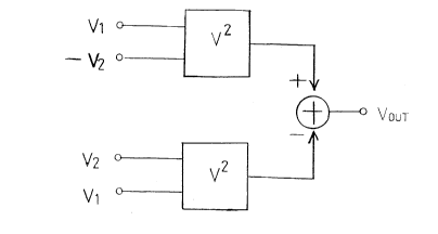
Fig. 3 schematically shows a multiplier according to
first to sixth embodiments of this invention. In Fig. 3, as
each squaring circuit has a differential input terminal
pair, a differential input voltage of a first squaring
circuit becomes (VltV2), and that of a second squaring
circuit becomes (V2-Vl). As a result, the outputs of these
two squaring circuits are subtracted to generate an output
voltage VOUT, which can be expressed as follows;
VOUT = (VltV2) 2 - (V2-Vl) 2
= 4VI-V2 .... ---- (21)
20S2875
That is, the output voltage VOUT can be expressed by
the product (Vl V2) of the first input voltage Vl and the
second input voltage V2, which means that such a circuit
that comprises two squaring circuits as shown in Fig. 3 has
a multiplier characteristic.
[First Embodiment~
Fig. 4 shows a multiplier according to a first
embodiment of this invention. This multiplier basically
comprises four sets of differential transistor pairs
respectively consisting of differential transistor pairs
(Ql and Q2), (Q3 and Q4), (Q5 and Q6), and (Q7 and Q8) whose
emitters are connected in common. In this case, if the
emitter size of each of one transistors Q2, Q3, Q6 and Q7 of
respective four sets of them is made one (1), that of the
other transistors Ql, Q4, Q5 and Q8 is made K times (K>l).
Also, two sets of differential transistor pairs consisting
of the transistors Ql and Q2 and the transistors Q3 and Q4,
and the two sets of differential transistor pairs consisting
of the transistors Q5 and Q6 and the transistors Q7 and Q8
form squaring circuits, respectively. These squaring
- 23 -
206287S
circuits are supplied with respective electric currents in
parallel, and an input signal (voltage VA) to be applied to
one differential input terminal pair (1 and 2) is opposite
in phase to an input signal (voltage VB) to be applied to
the other differential input pair (3 and 4).
In the two squaring circuits which consist respectively
of the two sets of transistor pairs (Ql and Q2) and (Q3 and
Q4) and two sets of transistor pairs (Q5 and Q6) and (Q7 and
Q8), the bases of the transistors whose emitter sizes are
different from each other, that is, of the transistors Ql
and Q3, Q2 and Q4, Q6 and Q8, and Q5 and Q7 are connected in
common, and the bases of the transistors Ql and Q3 are
connected to one input terminal 1 of the differential input
terminal pair (1 and 2), and the bases of the transistors
Q2 and Q4 are connected to the other input terminal 2
thereof. In addition, the bases of the transistors Q5
and Q7 are connected to one input terminal 3 of the
differential input terminal pair (3 and 4), and the bases of
the transistors Q6 and Q8 are connected to the other input
terminal 4 thereof. Also, the collectors of the transistors
whose emitter sizes are equal to each other, that is, of the
four transistors Ql and Q4, Q6 and Q7 and of the four
-- 24 --
206287S
transistors Q2 and Q3, and Q5 and Q8 are connected in
common to form differential output signals Ip and Iq,
respectively. The transistor pairs are connected to
respective constant electric current sources IO.
In the multiplier thus obtained, the collector currents
ICl and IC2 of the differential transistor pair Ql and Q2
can be expressed as follows;
a F IO
ICl = (22)
lt(l/k) exp(-VA/VT)
a F IO
IC2 = ...... ---- (23)
ltk exp(VA/VT)
where, a F IO can be expressed as follows;
a F IO = ICl t IC2 ............ ..(24)
Hence, the difference between the collector currents,
(ICl - IC2), can be expressed as follows;
ICl - IC2
- 25 -
206287S
kl'2 exp (VA/2VT) - (l/k) exp (-VA/2VT)
= a F IO
k 1/ 2 exp-(VA/2VT) t (l/k) exp (-VA/2VT)
...... -- (25)
Here, supposing that VK is expressed as;
VK = VT-ln(K) ------------- (26),
K can be obtained as follows;
K = exp-(VK/VT) ------------ (27)
Thus, Eq. (25) showing the difference between the
collector currents ICl and IC2 can be expressed by the
following equation (28);
ICl - IC2
exp-{(VAtVK)/2VT} - exp-{(-VA+VK)/2VT~
= a F IO
exp {(VAtVK)/2VT~ t exp {(-VAtVK)/2VT}
= a F IO tanh{(VAtVK)/2VT} -------- (28)
- 26 -
206287S
Next, the difference between the collector currents IC3
and IC4 of respective differential transistor pair Q3 and Q4
can be obtained in the same way as shown above, that is,
IC4 - IC3 = a F IO tanh{(-VAtVK)/2VT}
= -a F IO tanh{(VA-VK)/2VT} ----- (29)
Here, if the sum of Eq. (28) and Eq. (29) is IA, it
can be expressed as follows;
IA = IK - IU = (ICl-IC2) t (IC4-IC3)
= a F IO [tanh{(VAtVK)/2VT} - tanh{(VA-VK)/2VT}]
---------- (30)
Then, tanh x can be expanded as shown in Eq. (14) when
I xl < < 1, so that whenl VAtVKI 2VT and I VA-VKI 2VT,
Eq. (30) becomes as shown by the following equation(31),
resulting in being obtainable a differential electric
current proportional to the square of the input voltage VA.
Accordingly, it can be found that a squaring circuit can be
obtained by combiningly using two sets of unbalanced
differential transistor pairs having an emitter size ratio
2062875
of K:l.
IA = (ICl-IC2j + (IC4-IC3)
= a F IO [{(VAtVK)/2VT-(1/3) {(VA+VK)/2VT}33 --
- {(VA-VK)/2VT-(l/3)((VAtVK)/2VT)3}~ --
= a F IO {(VK/VT)-(VK/8VT3) VA2-(l/3)(VK/2VT)3 }
...... - (31)
Fig. 5 is an output characteristic diagram of the
squaring circuit shown in Fig. 4, in which SPICE simulation
values are graphically shown with the K as a parameter.
From Fig. 5, it can be found that good squaring
characteristic is provided.
Similar to the above explanations, for the transistor
pairs (Q5 and Q6) and (Q7 and Q8), the following equations
(32), (33) and (34) can be established, and the differential
electric current ~ IB between both the differential
transistor pairs can be found to be proportional to the
square of the input voltage VB as;
IC5 - IC6 = -a F IO tanh{(VB-VK)/2VT} ------ (32)
IC8 - IC7 = a F IO tanh{(VB+VK)/2VT} (33)
- 28 -
20S2~7~
IB = (IC5-IC6) + (IC8-IC7)
= - a F IO {(VK/VT)-(VK/8VT3)-VBZ-(l/3)(VK/2VT)3 --}
-------- (34)
As a result, if the sum of the differential electric
currents, ~ IA t ~ IB, is expressed ~ I, the following
equation can be established as;
IA t ~ IB
. { - ( a F-IO-VK)/8VT~-(VA a -VB 2 ) ( 35)
And, if the input voltages VA and VB are expressed as;
VA = Vl - V2 --------- (36)
VB = Vl t V2 ............ (37)
Eq. (35) can be expressed by the following equation (38),
which means that a differential current I proportional to
the product of the voltages Vl and V2 can be obtained, thus
being obtainable a multiplier.
- 29 -
2 0 6 2 8 7 5
~ I . a F IO (VK/2VT) Vl V2 ------- (38)
Fig. 6 is a characteristic diagram of a differential
output current I using a hyperbolic tangent function. From
this, it can be found that good multiplier characteristic is
obtainable in the range of an input voltage smaller than VK.
Fig. 7 is a gain characteristic diagram of the
multiplier which is obtained by differentiating the
differential output current ~ I using a hyperbolic tangent
function with respect to the first input voltage Vl. From
this, it can be found that good multiplier characteristic is
obtainable in the range of an input voltage smaller than VK.
Fig. 8 shows the result obtained from a multiplier
whose individual components were produced as K = 7. The
transistor used was of 2SC2785 produced by NEC. From this,
it can be found that though an offset is appeared in the
output because these components are realized on an
individual basis, good multiplier characteristic is
obtainable. In addition, this diagram was prepared in such a
manner that V2 was changed as a parameter from zero (0) to
100 mV in a step manner at an interval of 20 mV, and
- 30 -
206287~
converted into voltage as follows;
VMl = VCC - RL-Ip
VM2 = VCC - RL-Iq
[Second Embodiment]
Fig. 9 shows a squaring circuit to be used for
a multiplier according to a second embodiment of this
invention. This multiplier comprises two squaring circuits
as shown in Fig. 4. The squaring circuit to be used for this
embodiment is substantially equal in structure to that in
the first embodiment shown in Fig. 4. What is different
from the first embodiment is that respective transistors (Ql
and Q2) and (Q3 and Q4) forming two sets of differential
transistor pairs have emitter resistors. The transistors Q2
and Q3 with an emitter size of 1 have emitter resistors
with a resistant value of R, and the transistors Ql and Q4
with an emitter size of K have emitter resistors with a
resistant value of (R/K) which is inversely proportional to
be the emitter size ratio.
The operational characteristic of this squaring circuit
206~875
cannot be analytically resolved because of including emitter
resistors into differential transistor pairs. As a result,
SPICE simulation values were obtained using the product
(R IO) of the resistant value R of the emitter resistance
and the current value IO of the driving current source as a
parameter, which is shown in Fig. 10. From Fig. 10, it can
be found that the range of input voltage can be expanded and
yet good squaring characteristic can be obtained by
appropriately selecting the value of the product(R IO).
Next, with K = 3, and R IO = 8.6VT, experiments were
carried out using individual components, the result of which
is shown in Fig. 11. The transistors used was of 2SC2785.
From Fig. 11, it can be found that though an offset is
appeared in the output because these components are realized
on an individual basis, good multiplier characteristic is
obtainable. In addition, this diagram was prepared in such
a manner that V2 was changed as a parameter from zero (O) to
400 mV in a step manner at an interval of 100 mV. Compared
with the result shown in Fig. 8, it can be found that the
input voltage range in Fig. 11 is expanded approximately
three times. As a result, a multiplier using the squaring
circuit having emitter resistors as shown in Fig. 9 makes
- 32 -
2062875
obtainable good characteristic and yet advantageously
expanded input voltage range.
[Third Embodiment]
Fig.12 is a circuit diagram of a squaring circuit to be
used for a multiplier according to a third embodiment of
this invention, which comprises two squaring circuits
combinedly arranged as shown in Fig. 4. This squaring
circuit is substantially equal in structure to that in the
first embodiment shown in Fig. 4 excepting that respective
transistors (Ql and Q2) and (Q3 and Q4) forming two sets of
differential transistor pairs have emitter resistors on
their one transistors. That is, the transistors Q2 and Q3
with an emitter size of 1 each has an emitter resistor with
a resistant value of R and the transistors Ql and Q4 with an
emitter size of K each does not have an emitter resistor.
The operational characteristic of this squaring circuit
cannot be analytically resolved because of including emitter
resistors into differential transistor pairs. As a result,
SPICE simulation values were obtained using product (R IO)
of the resistant value R of the emitter resistor and the
current value IO of the driving current source as a
2062875
parameter, which is shown in Fig. 13. From Fig. 13, it can
be found that the range of the input voltage can be expanded
and yet good squaring characteristic can be obtained by
appropriately selecting the value of the product (R IO).
Next, with K = 3 and (R IO) = 8.6 VT, experiments were
carried out using individual components, the result of which
is shown in Fig. 14. What was used for this purpose was
2SC2785 transistor. From Fig. 14, it can be found that
though an offset is appeared in the output because these
components are individually realized, good multiplier
characteristic is obtainable. In addition, this diagram was
prepared in such a manner that V2 was changed as a parameter
from zero (O) to 400 mV in a step manner at an interval of
100 mV. Compared with the result shown in Fig. 8, it can be
found that the input voltage range in Fig. 14 is expanded
approximately four times. As a result, a multiplier using
the squaring circuit having emitter resistors as shown Fig.
12 makes obtainable good characteristic and yet
advantageously expanded input voltage range.
[Fourth Embodiment]
Fig. 15 shows a squaring circuit to be used for a
- 34 -
2062875
multiplier according to a fourth embodiment of this
invention, which comprises two squaring circuit combinedly
arranged as shown in Fig. 4, and substantially equal in
structure to that in the first embodiment shown in Fig. 4
excepting that respective transistors (Ql and Q2) and (Q3
and Q4) forming two sets of differential transistor pairs
have the same emitter size and yet only the transistors Q2
and Q4 have emitter resistors, respectively.
The operational characteristic of this squaring circuit
cannot be analytically resolved because including emitter
resistors into differential transistor pairs. As a result,
SPICE simulation values were obtained using the product
(R IO) of the resistant value R of the emitter resistor and
the current value IO of the driving current source as a
parameter, which is shown in Fig. 16. From Fig. 16, it can
be found that the input voltage range can be expanded and
yet good squaring characteristic can be obtained by
approximately selecting the value of the product (R IO).
Next, with K = 3 and (R IO) = 8.6VT, experiments were
carried out using individual components, the result of which
is shown in Fig. 17. The transistor used in the experiments
was of 2SC2785. From Fig. 17, it can be found that though
- 35 -
2062875
there appears an offset in the output because these
components were individually realized, good multiplier
characteristic is obtainable. In addition, this diagram was
prepared in such a manner that V2 was changed as a parameter
from zero (O) to 400 mV in a step manner at an interval of
100 mV. Compared with the result shown in Fig. 8, it can be
found that the input voltage range is expanded approximately
three times. As a result, a multiplier using the squaring
circuit having emitter resistors as shown in Fig. 15 makes
obtainable good multiplier characteristic and advantageously
expanded input voltage range.
[Fifth Embodiment]
Fig. 18 shows a squaring circuit to be used for a
multiplier according to a fifth embodiment of this
invention, which comprises two squaring circuits combinedly
arranged as shown in Fig. 4, and substantially equal in
structure to that in the first embodiment shown in Fig.
4 excepting that two sets of differential transistor pairs
respectively have transistors (Qla and Qlb) and (Q4a and
Q4b) having a Darlington connection. The transistors Qla,
Qlb, Q2, Q3, Q4a and Q4b are equal in emitter size and the
- 36 -
2062875
transistors Q2 and Q3 each has an emitter resistor with a
resistant value of R.
The operational characteristic cannot be analytically
resolved because of including emitter resistances into
differential transistor pairs. As a result, SPICE
simulation values were obtained using the product (R I0) of
the resistant value R of the emitter resistor and the
current value I0 of the driving current source as a
parameter, which is shown in Fig. 19. From Fig. 19, it can
be found that the input voltage range can be expanded and
yet good squaring characteristic can be obtained by
appropriately selecting the value of the product (R I0).
Next, with K = 3 and (R I0) = 8.6VT, experiments were
carried out using individual components, the result of which
is shown in Fig. 20. The transistor used for the experiments
was of 2SC2785. From Fig. 20, it can be found that though
there appears an offset in the output because these
components were individually realized, good multiplier
characteristic is obtainable. In addition, this diagram was
prepared in such a manner that V2 was changed as a parameter
from zero (0) to 400 mV in a step manner at an interval of
100 mV. Compared with the result shown in Fig. 8, it can be
206287~
found that the input voltage range is expanded approximately
five times. As a result, a multiplier using the squaring
circuit having emitter resistors as shown in Fig. 18 makes
obtainable good multiplier characteristic and yet
advantageously expanded input voltage range.
[Sixth Embodiment]
Fig. 21 shows a multiplier according to a sixth
embodiment of this invention, which is structured basically
in the same manner as in the first embodiment in that four
sets of differential transistor pairs (Q21 and Q22), (Q23
and Q24), (Q25 and Q26) and (Q27 and Q28) having emitters
connected in common are combinedly structured. In this
embodiment, the differential transistor pairs are
respectively supplied with electric current in parallel, and
if the emitter size of each of one transistors Q22, Q23, Q26
and Q27 is made one (1), that of each of the other
transistors Q21, Q24, Q25 and Q28 is made K (K>l).
In addition, in this embodiment, the differential input
terminal pair (1 and 2), and differential input terminal
pair (3 and 4) are applied with input signals (voltages V21
and V22), respectively, which are equal in phase.
- 38 -
206287~
The four sets of differential transistor pairs as shown
above are combinedly arranged in such a manner that the
bases of the transistors (Q21 and Q27), (Q22 and Q25), (Q23
and Q28) and (Q24 and Q26), which are respectively unequal
in emitter size to each other, are respectively connected in
common, and the base of the transistor Q21 and that of the
transistor Q27 are connected to the input terminal 1 of the
differential input terminal pair (1 and 2) and the base of
the transistor Q24 and that of the transistor Q26 are
connected to the input terminal 2 of the differential input
terminal pair (1 and 2). In addition, the base of the
transistor Q24 and that of the transistor Q25 are connected
to the input terminal 3 of the differential input terminal
pair (3 and 4), and the base of the transistor Q23 and that
of the transistor Q28 are connected to the input terminal 4
of the differential input terminal pair (3 and 4). On the
other hand, the collectors of the four transistors Q21, Q24,
Q26 and Q27 and those of the transistors Q22, Q23, Q25 and
Q28 are connected in common to form differential outputs Ip
and Iq, respectively. In addition, each differential
transistor pair is connected to the constant current source
I0.
- 39 -
2062875
Here, if the reference voltage is expressed as VR,
respective base voltages VB21, VB22, VB23, VB24, VB25, VB26,
VB27 and VB28 of the transistors of a first differential
transistor pair Q21 and Q22, a second differential
transistor pair Q23 and Q24, a third differential transistor
pair Q25 and Q26, and a fourth differential transistor pair
Q27 and Q28 can be expressed as follows;
VB21 = VB27 = VR t (1/2)V21 (39)
VB22 = VB25 = VR t (1/2)V22 ------ (40)
VB23 = VB28 = VR - (1/2)V22 ........... -- (41)
VB24 = VB26 = VR - (1/2)V21 ........... -- (42)
Here, the inter-base voltage of the first differential
transistor pair Q21 and Q22, and the inter-base voltage of
the second differential transistor pair Q23 and Q24 can be
expressed by the following equations (43) and (44), and the
both are equal to each other as shown by the following
equation (45), which is defined as VA for matching the first
- 40 -
20fi2875
embodiment;
VB21 - VB22 = (1/2) (V21-V22) ------ (43)
VB23 - VB24 = (1/2) (V21-V22) ------ (44)
VB21 - VB22 = VB23 - VB24 = VA = (1/2) (V21-V22)
------ (45)
In addition, the inter-base voltage of the third
differential transistor pair (Q27 and Q28), and that of the
fourth differential transistor pair (Q25 and Q26) can be
expressed by the following equations (46) and (47), and the
both are equal to each other as shown by the following
equation (48), which is defined as VB for matching the first
embodiment;
VB26 - VB25 = (-1/2) (V21+V22) ........ -- (46)
VB28 - VB27 = (-1/2) (V21+V22) ------ (47)
VB26 - VB25 = VB28 - VB27 = VB = (-1/2) (V21+V22)
..... -- (48)
- 41 -
2062875
Then, substituting VA and VB into Eq. (35), the
following equation (49) can be obtained, which means that a
differential current proportional to the product of the
input voltages V12 and V22, thus being obtainable a
multiplier circuit;
a F IO VK/8VT) X
[{(1/2)(V21-V22)} 2 - {(-1/2)(V21-V22)~ 2]
= a F IO (VK/4VT) V21 V22 ------ (49)
In addition, the differential current ~ I can be
expressed as ~ I = Ip-Iq in Figs. 4 and 21. In this case,
however, due to the fact that the currents Ip and Iq are
opposite in phase to each other, each of them includes such
a current component as the product of the voltages Vl (V21)
and V2 (V22). However, the magnitude thereof will become
only half the differential current ~ I.
Even in this embodiment, such squaring circuits as
shown in the second through fifth embodiments (see Figs. 9,
12, 15 and 18) can be used instead of each squaring circuit
- 42 -
2062875
shown in Fig. 2l. As a result, the input voltage range can
be expanded.
As explained above, according to the first through
sixth embodiments, four sets of differential transistor
pairs are not so arranged in a stack manner as in the prior
art, but arranged so-called in a line transversally thereby
allowing them to be operated at the same source voltage, so
that the multipliers shown above can be effectively operated
at lower source voltage than those in the prior art.
[Seventh Embodiment]
Fig. 22 schematically shows a multiplier according to a
seventh embodiment of this invention. In Fig. 22, three
squaring circuits each has a differential input terminal
pair, and a differential input voltage of a first squaring
circuit becomes (Vl-V2), a differential input voltage of a
second squaring circuit becomes Vl and a differential input
voltage of a third squaring circuit becomes V2. As a
result, an output voltage VOUT of the three squaring
circuits can be expressed as follows;
VOUT = -(Vl-V2) 2 + Vl 2 t V2 2
- 43 -
2062875
= 2Vl-V2 ...................... (50)
This means that the output VOUT can be expressed in
terms of the product (Vl V2) of respective output voltages
Vl and V2 of the first and second squaring circuits, and it
can be found that the circuit shown in Fig. 22 has a
multiplier characteristic as the case of the two squaring
circuits shown in Fig. 3.
Fig. 23 is a circuit diagram of the multiplier of this
embodiment. This multiplier basically comprises six
unbalanced differential transistor pairs (Ql and Q2), (Q3
and Q4), (Q5 and Q6), (Q7 and Q8), (Q9 and Q10) and (Qll and
Q12), whose emitters are connected in common, respectively.
Here, if the emitter size of each of one transistors Q2, Q3,
Q6, Q7, Q10 and Qll is made one (1), that of each of the
other transistors Ql, Q4, Q5, Q8, Q9 and Q12 is made K
(K>l). In addition, two sets of the transistor pairs (Ql and
Q2) and (Q3 and Q4), two sets of the transistor pairs (Q5
and Q6) and (Q7 and Q8) and two sets of the transistor pairs
(Q9 and Q10) and (Qll and Q12) respectively constitute
squaring circuits and supplied with electric current
in parallel to be driven by a constant current source I0.
- 44 -
2062875
In the three squaring circuits shown above, two sets of
unbalanced differential transistor pairs of each squaring
circuit are structured so that the collectors of the
transistors (Ql and Q4), (Q2 and Q3), (Q5 and Q8), (Q6 and
Q7), (Q9 and Q12) and (Q10 and Qll), which are respectively
equal in emitter size to each other, are connected in
common, and the bases of the transistors (Ql and Q3), (Q2
and Q4), (Q5 and Q7), (Q6 and Q8), (Q8 and Qll) and (Q10 and
Q12), which are respectively unequal in emitter size to each
other, are connected in common.
In addition, referring to the inter-relation between
the three squaring circuits, the bases of the transistors Ql
and Q3 of the two sets of unbalanced differential transistor
pairs (Ql and Q2) and (Q3 and Q4) as the first squaring
circuit and the those of the transistors Q5 and Q7 of the
two sets of unbalanced differential transistor pairs (Q5 and
Q6) and (Q7 and Q8) as the second squaring circuit are
connected in common to the first input terminal 1, the bases
of the transistors Q2 and Q4 of the first squaring circuit
and those of the transistors Q9 and Qll of the two sets of
the unbalanced differential transistor pairs (Q9 and Q10)
and (Qll and Q12) are connected in common to the input
- 45 -
2062875
terminal 2, and the bases of the transistors Q6 and Q8 of
the second squaring circuit and those of the transistors Q10
and Q12 of the third squaring circuit are connected in
common to the common input terminal 3.
In addition, the collectors of the transistors (Q5, Q8,
Q9 and Q12) and (Q6, Q7, Q10 and Qll), which are equal in
emitter size to each other in respective second and third
squaring circuits, are connected in common, which are
connected to the collectors of the transistors not equal in
emitter size to each other of the first squaring circuit,
respectively, thereby making the differential output
currents Ip' and Iq'.
Also, the input terminal 1 and the common input
terminal 3 makes a first input terminal pair to be applied
with one input signal voltage Vl and the input terminal 2
and the common input terminal 3 makes a second input
terminal pair to be applied with the other input signal
voltage V2, and as shown in Fig. 23, to the input terminals
1 and 2, the polarity of one of two input signals is
applied, and to the common input terminal 3, the polarity of
the other thereof is applied.
With the structure as shown above, the differential
- 46 -
2062875
currents IA and IB of the unbalanced differential transistor
pairs (Ql and Q2), (Q3 and Q4), (Q5 and Q6) and (Q7 and Q8)
can be obtained in the same way as in the first embodiment
(see Eqs. (30) and (34)). Next, those of the unbalanced
differential transistor pairs (Q9 and Q10) and (Qll and Q12)
can be obtained similarly by the following equations (51)
and (52), so that the differential current IC of the both
pairs can be expressed by the following equation (53),
showing that it is proportional to the square of the input
voltage V2.
IC9 - IC10 = a F IO tanh {(V2+VK)/2VT~ ..... (51)
IC12 - ICll = - a F IO tanh {(V2-VK)/2VT} (52)
IC = (IC9tIC12) - (IClOtICll)
= (IC9-IC10) t (IC12-ICll)
= a F IO [tanh {(V2tVK)/2VT} - tanh{(V2-VK)/2VT}]
= a F IO {(VK/VT)-(VK/4VT3)V2 2 - (2/3)(VK/2VT) 3 }
---- (53)
As a result, in Fig. 23, if the difference (Ip'-Iq') of
- 47 -
2062875
the differential output currents Ip' and Iq' is expressed as
I', the following equation will be obtained;
I' = Ip' - Iq'
= - ~ IA + ~ IB t ~ IC
= a F IO X
[(VK/VT)-(2/3)(VK/2VT)3-(VK/4VT3) (V12+V22-(Vl-V2) 2} ]
= - a F IO X
[(VK/VT)-(2/3)(VK/2VT)3-(VK/2VT3) Vl V2 ]
----- (54)
Here, as VA = Vl-V2, VB = Vl and VC = V2, the following
equation (55) can be obtained;
I' . a F IO [(VK/2VT3) Vl V2 - {(VK/VT)-(2/3)(VK/2VT) 2 ~ ]
(55)
This means that the differential current ~I
proportional to the product (Vl V2) of the input voltages Vl
and V2, resulting in obtaining a multiplier circuit.
[Eighth Embodiment]
- 48 -
2062875
Fig. 24 is a multiplier according to an eighth
embodiment of this invention, which comprises squaring
circuits having one squaring circuit added to the multiplier
of the seventh embodiment, and for the sake of convenience
of explanations, the transistors are indicated by the
sequential reference numerals.
The multiplier of this embodiment basically comprises
eight unbalanced differential transistor pairs (Ql and Q2),
(Q3 and Q4), (Q5 and Q6), (Q7 and Q8), (Q9 and Q10), (Qll
and Q12), (Q13 and Q14) and (Q15 and Q16) respectively
having the emitters connected in common. Here, if the
emitter size of each of one transistors Q2, Q3, Q6, Q7, Q10,
Qll, Q14 and Q15 of the eight pairs is made one (1), the
emitter size of each of the other transistors Ql, Q4, Q5,
Q8, Q9, Q12, Q13 and Q16 is made K (K>l). In addition, two
sets of the pairs (Ql and Q2) and (Q3 and Q4), two sets of
the pairs (Q5 and Q6) and (Q7 and Q8), two sets of the pairs
(Q9 and Q10) and (Qll and Q12), and two sets of the pairs
(Q13 and Q14) and (Q15 and Q16) respectively form squaring
circuits and supplied with source currents in parallel to be
driven by the constant current source IO.
In the four squaring circuit shown above, two sets of
- 49 -
2062875
unbalanced differential transistor pairs of each squaring
circuit are structured so that the collectors of the
transistors (Ql and Q4), (Q2 and Q3), (Q5 and Q8), (Q6 and
Q7), (Q9 and Q12), (Q10 and Qll), (Q13 and Q16) and (Q14 and
Q15), which are respectively equal in emitter size to each
other, are connected in common, and the bases of the
transistors (Ql and Q3), (Q2 and Q4), (Q5 and Q7), (Q6 and
Q8), (Q9 and Qll), (Q10 and Q12), (Q13 and Q15) and (Q14 and
Q16), which are not equal in emitter size to each other, are
connected in common.
In addition, referring to the inter-relation of the
four squaring circuits shown above, the bases of the
transistors Ql and Q3 of the two sets of unbalanced
differential transistor pairs (Ql and Q2) and (Q3 and. Q4) as
the first squaring circuit and those of the transistors Q5
and Q7 of the two sets of unbalanced differential transistor
pairs (Q5 and Q6) and (Q7 and Q8) as the second squaring
circuit are connected in common to the input terminal 1, the
bases of the transistors Q2 and Q4 of the first squaring
circuit and those of the transistors Q9 and Qll of the two
sets of unbalanced differential transistor pairs (Q9 and
Q10) and (Qll and Q12) are connected in common to the input
- 50 -
2062875
terminal 2, the bases of the transistors Q6 and Q8 of the
second squaring circuit and those of the transistors Q14 and
Q16 of the third squaring circuit are connected in common to
the common input terminal 3, and the bases of the
transistors Q13 and Q15 of the third squaring circuit and
those of the transistors Q12 and Q10 of the fourth squaring
circuit are connected in common to each other. The bases of
the transistors Q13 and Q14 are connected in common to each
other.
Further, the collectors of the transistors (Ql and Q4),
(Q13 and Q16), (Q3 and Q2), (Q14 and Q15), (Q5 and Q8), (Q12
and Q9) , (Q6 and Q7), and (Q10 and Qll), which are
respectively equal in emitter size to each other, are
connected in common, and the collectors of the transistors
(Ql, Q4, Q13 and Q16), (Q6, Q7, Q10 and Qll), (Q3, Q2, Q14
and Q15) and (Q12, Q8, Q5 and Q9), which are respectively
not equal in emitter size to each other, are connected in
common, thereby forming the differential output currents Ip"
and Iq".
Also, similar to the case of the seventh embodiment,
the input terminal 1 and the common input terminal 3 makes
a first input terminal pair to be applied with one input
- 51 -
2062875
signal (voltage Vl) and the input terminal 2 and the common
input terminal 3 makes a second input terminal pair to be
applied with the other input signal (voltage V2), and as
shown in Fig. 24, to the input terminals 1 and 2, the
polarity of one of two input signals is applied, and to the
common input terminal 3, the polarity of the other thereof
is applied.
With the structure as shown above, in the fourth
squaring circuit additionally provided, that is, the two
sets of unbalanced differential transistor pairs (Q13 and
Q14) and (Q15 and Q16), the collector currents (IC13 and
IC14) and (IC15 and IC16) and their differential currents
(IC13-IC14) and (IC16-IC15) can be obtained as follows and
the differential current ~ ID between the both can be
expressed as follows;
IC13 - IC14 = a F IO tanh (VK/2VT) ----- (56)
IC16 - IC15 = a F IO tanh (VK/2VT) ----- (57)
ID = 2 a F IO tanh (VK/2VT)
= 2 a F IO {(VK/2VT) - (1/3)(VK/2VT) 3 }
- 52 -
2062875
= a F IO {(VK/VT) - (2/3)(VK/2VT)3
....... ---(58)
As a result, in Fig. 24, if the difference (Ip"-Iq") of
the differential output currents Ip" and Iq" is expressed as
I", it can be expressed by the following equation (59);
I" = Ip" - Iq"
= - ~ IA t ~ IB t ~ IC - ~ ID
= a F-I0-(VK/2VT3)-Vl-v2 ........... ........ (59)
As a result, the direct current term of Eq. (55) that
is, -a F IO [(VK/VT)-(2/3)(VK/2VT)2], can be cancelled, thus
being capable of being approximated by the following
equation (60);
I ' . a F IO (VK/2VT3) Vl V2 ......... - (60)
Therefore, in the same way as in the first embodiment,
the differential current ~ I" proportional to the product
(Vl V2) of the input voltages Vl and V2 can be obtained,
which means that a multiplier circuit can be obtained. In
- 53 -
2062875
addition, the multiplier characteristic of this embodiment
was analyzed in terms of hyperbolic tangent function, the
result of which is shown in Fig. 25.
Even in the seventh and eighth embodiments of this
invention, the squaring circuits described in the second
through fifth embodiments can be used instead of those shown
in Figs. 23 and 24 (see Figs. 9, 12, 15 and 18). As a
result, the input voltage range can be advantageously
expanded.
As explained above, in case of the multipliers shown in
the seventh and eighth embodiments, six or eight unbalanced
differential transistor pairs are not arranged in a stuck
manner as in the prior art, but arranged so-called in a line
transversally, thereby allowing them to be operated at the
same source voltage, so that the multipliers shown above can
be effectively operated at lower source voltage than those
in the prior art.
[Ninth Embodiment]
Fig. 26 shows a squaring circuit to be used for a
multiplier according to a ninth embodiment of this
invention, which comprises four MOS transistors. In Fig. 26,
206287S
MOS transistors Ml and M2 form a first differential
transistor pair to be driven by a constant current
source I0, and MOS transistors M3 and M4 form a second
differential transistor pair to be driven by a constant
current source in conformity with the following equation
(61);
{2 H1~2 / (Htl)}-I0 ............. --- (61)
Referring to the inter-relation between the both
differential transistor pairs, the drains of the transistors
Ml and M3 and those of the transistors M2 and M4 are
connected in common, and the gates of the transistors Ml and
M4 and and those of the transistors M2 and M3 are connected
in common respectively.
Here, in the first transistor pair, the transistor Ml
has a ratio of a gate width Wl and gate length Ll, or Wl/Ll,
of one (1), and the transistor M2 has a ratio of gate width
W2 and gate length L2, or W2/L2, of H. Namely, H can be exp
ressed as follows;
(W2/L2)/(Wl/Ll) = H (H ~ 1) ------ (62)
206287~
On the other hand, in the second differential
transistor pair, the transistor M3 has a ratio of gate width
and gate length, or W3/L3, and the transistor M4 has a
ratio of gate width and gate length, or W4/L4, which are
equal to each other as shown below;
(W3/L3) = (W4/L4) = 4H- Hl/2/(Htl)2 ------ (63)
Thus, respective drain currents Idl and Id2 of the
transistors Ml and M2 of the first differential transistor
pair can be expressed as follows;
Idl = ~ n (COX/2) (Wl/Ll) (VGSl-VT)2 ....... -- (64)
Id2 = ~ n (COX/2) H (Wl/Ll) (VGS2-VT)2 ------ (65)
In addition, the constant current source I0 and the
input voltage VlN can be respectively expressed as follows;
Idl + Id2 = I0 ------- (66)
- 56 -
2062875
VGSl - VGS2 = VIN ------- (67)
Here, if ~ Idp is expressed by the following equation
(68);
~ Idp = Idl - Id2 ------- (68),
it can be obtained as follows;
~ Idp =
-(l-l/H){(l+l/H)IO-2~ l-VIN2~t4~ l{(l+l/H)(IO/~ l)-VIN2)} 1/2
(l+l/H)2
..... --- (69)
where,
~ n (COX/2) (Wl/Ll) ----- (70)
Similarly, in the second differential transistor pair,
respective drain currents Id3 and Id4 of the transistors M3
and M4 can be expressed as follows;
2062875
Id3 = {4H- H1~2/(Htl)2} ~ l(VGS3 - VT)2 ------ (71)
Id4 = {4H- H1~2/(Htl)2} ~ l(VGS4 - VT)2 ------ (72)
In addition, the constant current source and the input
voltage VIN can be respectively expressed as follows;
Id3 t Id4 = (2 H1~2/(Htl)} IO ----- (73)
VGS4 - VGS3 = VIN ......
Here, if
IdQ = Id3 - Id4 ----- (75)
it can be obtained by the following equation (76);
IdQ = {-4H- H1~2/(Htl)2} ~ l VIN x
[4 {Hl/2-Io/(Htl)}.{(Htl)2/4H. H1'2-~ 1~ - VIN2]l~2
= -{4-~ l-(l/H1/2)/(Htl)2}-VIN X
~{4 Hl/2 IO/(H+l)} ~(H+1)2/4H Hl'2 ~ 1} - VIN2]l/2
..... -- (76)
- 58 -
2062875
As a result, the differential output current I can be
calculated by the following equation (77);
I = Il - I2 = ~ IdP - ~ IdQ
(l-l/H) {2~ l VIN2 - (ltl/H) IO}
(l+l/H) 2
= ~2H (H-l) ~ l/(Htl)2} VIN2 - ~(H-l)/(Htl)} IO
--------- (77)
That is, the differential output current proportional
to the square of the input voltage VIN can be obtained, thus
being obtainable a multiplier circuit.
As explained above, according to this embodiment, a
squaring circuit comprises two sets of differential
transistor pairs having gate width and gate length ratios
appropriately selected for making a differential input, so
that such a squaring circuit can be realized that is
completely independent of variation in threshold voltage due
to manufacturing dispersion of transistors. ~onsequently,
- 59 -
2062875
a squaring circuit adapted to be integrated on a large-scale
basis as well as to be preferably used for a multiplier can
be effectively provided.
- 60 -