Note: Descriptions are shown in the official language in which they were submitted.
2063000
METHOD AND CIRCUIT FOR DEMULTIPLEXING DIGITAL
SIGNALS CAPABLE OF ABSORBING DESTUFFING JITTER
R~GROUND OF THE lNV ~:N~l~IoN
Field of the Invention:
The present invention relates to a method and
circuit for demultiplexing digital signals which are
capable of absorbing destuffing jitters caused by
demultiplexing.
Description of Related Art:
Fig. 1 is a block diagram showing an example of
a digital signal demultiplexing circuit of the
conventional type.
Demultiplexing circuit 51 (hereinafter referred
to as "DMUX 51") receives higher order digital signals
structured in frames and demultiplexes them into lower
order signals. Analog IC 53 receives the lower order
digital signals demultiplexed by DMUX 51 and performs
smoothing thereof by means of inner memory 55 and
thereafter performs digital/analog conversion of the
signals. Transformer 54 executes unipolar/bipolar
conversion of the signals according to outputs of analog
IC 53.
However, the digital data demultiplexing circuit
of the conventional type described above is influenced by
the jitter absorption characteristic of the analog IC and
2063000
_ 2
generates errors when it receives jitters exceeding its
performance.
SUMMARY OF THE INVENTION
The present invention has been developed to
5 remove the problems of the conventional type circuit
described above, and its object is to provide a method and
circuit for demultiplexing digital signals which generate
no errors even when the signals exceeding the jitter
absorption capability of the analog IC of the circuit is
10 received.
In order to achieve the above object, the
digital signal demultiplexing method of the present
invention comprises a first step of demultiplexing frame-
structured higher order digital signals and separating
15 them into lower order digital signals, a second step of
digitally smoothing jitters, which are periodically
generated in the lower order signals, the smoothing being
performed by writing into a buffer memory the lower order
signals separated by demultiplexing and reading them out
20 from the buffer memory, a third step of resmoothing the
lower order signals which have been smoothed by the buffer
memory, and thereafter performing digital~analog
conversion thereof and a fourth step of performing
unipolar/bipolar conversion of the signals which have been
25 processed through digital/analog conversion thereof.
Further, the circuit for demultiplexing the
2063000
digital signals of the present invention comprises a
demultiplexing circuit for receiving the frame-structured
higher order digital signals and demultiplexing them into
lower order digital signals, a buffer memory for digitally
smoothing jitters, which are periodically generated in the
lower order signals demultiplexed by the demultiplexing
circuit, by the writing the lower order signals separated
by demultiplexing and reading them out, an analog IC for
finishing resmoothing of the lower order signals which had
been smoothed by the buffer memory and for performing
digital/analog conversion of the lower order signals and a
transformer for performing unipolar/bipolar conversion of
the signals which have already been processed through
digital/analog conversion thereof by means of the analog
IC.
Further, the circuit for demultiplexing the
digital signals of the present invention comprises a
demultiplexing circuit for receiving frame-structured
higher order digital signals, demultiplexing them into
lower order digital signals, separating the lower order
signals into groups, buffer memories, each of which
receives one of the groups of the lower order signals and
digitally smoothes the jitters which are periodically
generated in the received group of the lower order signals
25 demultiplexed by the demultiplexing circuit, by writing
the lower order signals separated by demultiplexing and
2063000
-- 4
reading them out, analog ICs, each of which is connected
to one of the smoothing buffer memories, each of which
resmoothes the signals which had been smoothed by the
buffer memory and performs digital/analog conversion of
the resmoothed lower order signals and transformers, each
of which is connected to one of the analog ICs, performing
unipolar/bipolar conversion of the signals which have
already been processed through digital/analog conversion
thereof by means of the analog IC connected to itself.
It is preferable that the buffer memory reads
out the lower order signals in synchronization with a read
clock other than a write clock with which the smoothing
buffer memory writes the above lower order signals.
Further preferably, the buffer memory performs
FIFO operation and the analog IC performs resmoothing in
synchronism with the read clock which is supplied to the
buffer memory, having an internal memory for resmoothing.
The smoothing in the present invention means an
arrangement of the pulse line to arrange it into equal
spaces which have become unequally spaced due to
destuffing operation of the stuffed signals.
The above and other objects, features and
advantages of the present invention will become apparent
from the following description referring to the
accompanying drawings which illustrate an example of a
preferred embodiment of the present invention.
2063000
BRIEF DESCRIPTION OF THE DRAWING
Fig. 1 is a block diagram showing an example of
the conventional type.
Fig. 2 is a block diagram showing an embodiment
5 of a circuit for demultiplexing digital data of the
present invention.
Fig. 3 is a block diagram showing an example of
an analog IC which is usable for the embodiment of Fig. 2.
Fig. 4 is a block diagram showing an embodiment
10 having lower order signal data divided into four (4)
systems.
DESCRIPTION OF THE PREFERRED EMBODIMENT
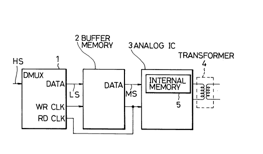
Demultiplex circuit 1 (hereinafter referred to
as "DMUX 1") demultiplexes frame-structured higher order
15 digital signals HS into lower order digital signals, and
by destuffing the stuffed pulses outputs them as lower
order digital signals LS together with write clock WR CLK
and read clock RD CLK.
Buffer memory 2 for smoothing writes destuffed
20 signals LS in synchronization with write clock WR CLK,
then reads written signals LS synchronizing with read
clock RD CLK and outputs them as signals MS. This
write/read action is performed by FIFO operation.
Therefore, jitters to be generated periodically
25 by demultiplexing by means of DMUX 1 can be digitally
substantially smoothed.
206300o
-- 6 --
Analog IC 3 receives signals MS inputted from
buffer memory 2, and performs smoothing of the signals by
using internal memory 5 and the successive digital/analog
conversion thereof, then outputs them to transformer 4
synchronizing with read clock RD CLK transmitted from DMUX
1.
Transformer 4 performs unipolar/bipolar
conversion of output signals transmitted from analog IC 3.
Therefore, even if lower order signals LS
contains jitters exceeding the jitter absorption capacity
of analog IC 3, no error is generated in the signal data
because the jitters have been previously reduced by means
of buffer memory 2.
Further, a concrete example of analog IC 3 will
15 be described below. As a typical example of analog IC 3,
there is T 7290 (or T 5290) of A T & T, as shown in Fig.
3. In this case, read clock RD CLK of the embodiment in
Fig. 2 should be supplied as a transmit clock (refer to
mark *) and signals MS should be supplied as a transmit
20 data (refer to mark *).
As for the case in which higher order signals
are demultiplexed into lower order signals of four
systems, it is preferable to construct the system as shown
in Fig. 4.
DMUX 11 outputs lower order signals Dl, D2, D3
and D4 of the four systems together with write clocks WRl,
206300~
_
-- 7
WR2, WR3, WR4 and read clocks RDl, RD2, RD3 and RD4,
respectively. Buffer memories 21, 22, 23 and 24 for
smoothing perform smoothing of the above signals Dl, D2,
D3 and D4, respectively, and analog ICs 31, 32, 33 and 34,
5 respectively, perform resmoothing thereof respectively.
After finishing digital/analog conversion,
the resmoothed signals are output through transformers 41,
42, 43 and 44, respectively.
Further, symbols DO+ and DO- of the buffer
10 memories 21, 22, 23 and 24 correspond to a positive
polarity and a negative polarity, respectively, of the
bipolar signals.
As can be understood from the above embodiment,
it becomes possible to eliminate data errors by providing
15 a buffer memory in the preceding stage of the analog IC
and having resistibility against destuffing jitters, even
though the destuffing jitters to be generated in the
demultiplexing operation exceed the jitter absorption
capacity of the analog IC.
It is to be understood that variations and
modifications of the method and circuit for demultiplexing
of the digital data of the present invention which are
capable of absorbing the destuffing jitters disclosed
herein will be evident to those skilled in the art. It is
25 intended that all such modifications and variations be
included within the scope of the appended claims.