Note: Descriptions are shown in the official language in which they were submitted.
902-089
~063~1
T.ll~, MONITO~n~G FO~ ,cn~ SI~ A~Ac
TFrr~cAr Ftprn
The invention concerns a process and device for 11. 1.. ,.. ." j
errors in a multiplex signal, structured according to CCITT P~ '
G.707, G.708 and G.709, in which a multiplex frame with a head part amd a
functional part are described.
BACKGROUNl~ OF T~rF~ r~VF~lTION
The essential . T~ of the new S~ , Digital Hierarchy
(SDH) are set fbrth in CCITT D~ c G.707, G.708 and G.709. As
with a~.y.. ~,l--u.. ~ h~ hil-c, the new a,~ hierarchy also contains
multiplex signals with different bit rate r.~u~ .. However, the multiplex sig-
nals of the synchronous digital hierarchy have other bit rate rl,, -' , and a
different frame structure as well.
The elemental multiplex signal of the synchronous digital hierarchy is
15 ~ , t . .~ 1 as an STM-1 signal (~ u~uu~ transport module) and has a bit
rate frequency of 155 kbitls. Other multiplex signals can be formed by byte
i.,t~ll~vii~g several STM-1 signals. These multiplex signals are called STM-N
signals, where N indicates the number of STM-1 signals. The frame structure of
the multiplex elements is byte oriented. One byte consists of eight bits. The
2û frame of the STM-1 signal consists of nine lines and ~70 columns for each one byte. The ~ " sequence is by bytes and lines from top to bottom. The
first nine columns contain the Section Overhead (SOH) - hereafter called head
part. The remaining columns of the STM-1 signal contain the Payload - hereafter
called functional part. No further details are provided, since the functional part's
25 structure is not essenfial to understand the inve~ltion.
20630a 1
The head part contalns slgnals assigned to a
transmission line, such as the frame identificatlon word,
which consists of 6 bytes, the synchronlzQtlon bytes Al, A2,
byte Bl, which serves to monitor a regeneration section, byte
Fl, which is transmltted by the service channel, or bytes for
nat lonal use .
To monltor a re~eneration section, the CCITT-
Rec~ - t ions G. 783 and G. 958 suggest measuring the
transnlssion error probablllty, and to form the parlty o~ the
bits from an entire frame, and then transmit these in the
following frame with the parlty word Bl. The parity word Bl
is then checked and newly formed by each intermediate
generat o r .
A well-known process, the Bit Interleaved Parity
(BIP) process, i8 used to determine the transmission error
probability. It produces an N-bit code, where N is a whole
number ~ integer), which ls elght ln the party word Bl .
Thls regulres an intermediate generator, which
complies with CCITT-Rec~ ion G.783 and G.958, needlng an
extensive circuit to determine the parity, and a device to
evaluate and describe the parity word Bl, in addit ion to a
synchronizatlon clrcult, and other signal processlng
lnstallatlons, such as a demultiplexer and a multiplexer.
The invent ion now has the task of creat ing a process
and a device to realize lt, maklng lt posslble, wlth slmple
means, to determlne the transmlsslon error probablllty during
the transmlssion of SDH signals.
-- 2 --
72430-180
A
-
~ 2 ~ D 1
6UMMARY OF THE INVEN~ION
Accordlng to one aspect, the present lnventlon
provides a process to determlne transmlsslon errors ln a
multlple~ slgnal for a Synchronous Dlgltal Hlerarchy slgnal,
structured accordlng to CCITT-R~c~ ' t.lons G.707, G.708 and
G.709, ln whlch a multlplex frame wlth a head part and a
functional part are descrlbed, and ln whlch frame
synchronlzatlon has been establlshed ln a recelvlng devlce,
comprlslng the steps of: retrlevlng at least one known word
located ln a known place ln the head part of the frame to be
checked for transmlsslon errors; and comparlng all blts of
sald at least one known word wlth at least one reference word
havlng a predetermlned value based on sald at least one known
word 80 that no computatlon 18 n~cPQ~ry to determlne sald at
least one reference word 80 as to derlve lnformatlon about a
transmlsslon error from the comparlson.
A speclal advantage of the lnventlon 18 that the
reduced number of ele~ents not only produces cost advantages,
but that the total requlrement of energy 18 conslderably
reduced, whlch 18 of speclal advantage e.g., when the clrcult
18 contalned ln lntermedlate regenerators, whlch must be
operated wlth thelr own energy supply.
Accordlng to another aspect, the present lnventlon
provldes a devlce to detect transmlsslon errors ln a multlple~
slgnal, whlch has a multlplex structure for a Synchronous
Dlgltal E~lerarchy slgnal accordlng to CCITT-Rf~c -~ tlons
G.707, G.708 and G.709, ln whlch a multlple~ frame wlth a head
part and a functlonal part are descrlbed, and whlch contalns a
-- 3 --
72430-180
-
20630al
synchronlzatlon clrcult for synchronlzlng the multiplex frame
wlth the devlce, comprlslng~ means for retrlevlng at least one
known word located ln a known place ln the head place in the
head part of the frame to be checked for transmlsslon errors:
means for comparlng all blts of sald at least one known word
wlth at least one reference word havlng a predetermlned value
based on sald at least one known word 80 that no computatlon
18 necessary to determlne sald at least one reference word;
and means for derlvlng lnformatlon about a transmlsslon error
from the comparlson, and for supplylng lt to an outlet.
Accordlng to yet another aspect, the present
lnventlon provldes a regenerator unlt I comprlslngs an optical
recelver, responslve to multlplex optlcal slgnals structured
ln a Synchronous Dlgltal Hlerarchy accordlng to CCITT-
~oc~ ` t lons G. 707, G. 708 and G. 709 having a head part and
a functlonal part, for providing recelved multlplex optlcal
slgnals; a regenerator, responslve to the recelved multlplex
optlcal slgnals, for provldlng regenerated multiplex optical
signals~ an optical transmltter, responsive to the regenerated
multiplex optlcal signals, for providing transmitted
regenerated multlplex optlcal slgnals; and transmlsslon error
detector meansl responslve to the recelved multlple~ optlcal
signalsl for comparlng all blts of a known word of data from
the head part of the recelved multlplex optical signals wlth a
reference word havlng a predetermlned value based on the known
word, for provldlng transmlsslon error detector slgnals,
whereby no computatlon 18 necessary to determine the reference
wo rd .
- 3a -
72430-180
A~`
~ 206300 1
BRIEF DESCRIPTION OF TE~E~ DRAWINGS
The followlng descrlbes conflguratlon e~amples vla
f lgures 1-7;
Fig. 1 shows a regenerator unlt according to the
lnventlon, ln block clrcult dlagram form.
Flg. 2 shows the head part of an 8TM-1 slgnal.
72430-180
~,
20~300 l 902-089
Fig. 3 shows a first ~ - example of a i error
detection according to the invention.
Fig. 4 shows a second c(-A~æ ~ example of a t, error
detection according to the invention/
S Fig. 5 shows the essential parts of a , station for several
lines, according to the invention.
Fig. 6 shows a section of a first i segment with several
" sections.
Fig. 7 shows a cutout of a second ~ -.. segment with several
~ - sections.
RFA~T MODE FQR C.~RRYING OIJ r T~F. INVFI~TION
Figure 1 shows a ~ GtUl unit RE according to the invention, in the
form of a schematic block circuit diagram. It only exhibits the essential compo-nents of the invention. ~ recciver OE, for receiving optical signals, is connected
15 on the receiving side to a beam wave guide, as 1"... - ~ line UL. The trans-
mission line UL transmits multiplex signals, which exhibit a multiplex structureaccording to CClTI-R~o~ - G.707, G.708 and G.709, and in which a
frame with a head part and a functional part are described. To simplify the
~IP~rrir~ the following starts with the l~ Of STM~ signals, although
20 the advantage of the invention for the l,~ of higher multiplex signals,
e.g. STM-16 signals, is more significant.
The receiver OE contains an optical-electrical converter, and ~ y
a circuit for timing and ~ g the receiver O~ with the frame, and there-
fore an outlet for a timing line TL and an outlet for a data line DL, in which the
25 STM signals are transmitted in series. The timing line TL and the data line DL
902-089
206300 1
are connected to a l~hl~ ul RG and the; error detection UE. In
turn, the ., RG is connected by data line DL and timing line TL to a
transmitter OS. The transmitter OS contains and electrical-optical converter andan outlet for a beam wave guide as the ~ line UL. The l . . ~
5 error detection UE may also be connected between . ~ RG and transmitter
OS by data line DL and timing line TL. The l~ ld~UI RG may also contain the
timing and aJI~ g circuit.
R~n~ tir~n of the bit flow wi~ regard to pulse wave shape, time and
amplitude takes place in well known form in l~ UI RG, without the need to
decompose the STM4 signal. R~ en.~rPti~m of the bit ~low, as such, is not the
subject of this invention, and is therefore not detailed any further.
D, of the l,. - ~: ". error probability is functionally
separated from the ,. ~. Ir ~ ,., of the bit flow, in a i error detection
UE, which is especially designed for this purpose. However, _ RG and
15 the ~ 11 error detection UE may be located in one unit.
To determine the i error probability, this invention requires
knowing the content and position of at least one word in the head part of the STM-
4 signal. This known word can also be retrieved as a reference word in the
error detection UE, and is then compared with the reference word.
20 The ~ --- error probability can then be derived from the results of the
Figure 2 shows the head part SOH of an STM signal. To simplify the
,C.~ iùll, the head part SOH of an STM-I signal is shown, which in princi-
ple also c~ to the head part of an STM-4 signal. For example, the frame
25 ;.l~ ;"" word is defined in the first line, and is used to a~ lllul~ the frame
beginning o~ the STM signal.
902-089
~06300 ~
The word consists of three ~ ul~ iol~ bytes Al and tbree syn-
~,llI~IIi~l~iUII bytes A2. The bh se~uence is always 11110110 for A1 and 001010-00 for A2. Tbis means that the frame i~ ifi~o~inn word, or only parts of it, aresuitable for use in ~ the ~ error probability.
5 A first ~1~ l fi ~.. ,.~;.. exatnple of a ~ .. error detection U~1 is
shown in figure 3. In the simplest case, it shows a slide register SR, to which tbe
bit flow in data line DL is transmitted and timed by timing line TL. Through a
parallel outlet in parallel line PLI, the slide register SR is connected to the ref-
erence word decoder RWD, in wbich tbe bit flow in the slide register SR is
10 compared with a reference word stored in the reference word decoder RWD. Tbe
reference word decoder RWD determines the result of tbe ~ ... by the
number of coinciding bits per word, or the number of - bits per
word, and transmits the result to an evaluation unit AE. In the simplest case, the
reference word consists of one byte, i.e. 8 bits, but otber word lengths may also
be submitted.
A second ~ ;.- of a i error detection UE2 is shown in
figure 4. It has a first slide register SR1 and a second slide register SR2, both of
which are connected to data line DL and timing line TL, where the bit flow goingto slide register SR1 is delayed by a time-lag deYice VG in data line DL, beforeslide register SR1. Slide register SRl is connected by a parallel outlet of parallel
line PL2 with slide register SR2, in such a way, that any conditions existing in tbe
slide registers can be compared with each other. S~ide register SR2 is expanded
by a decoder, which transmits the result of the r~mr~riC~n to an evaluation unitAE.
By contrast to the first, the second c~nfi~ll~ti~n of ~,.m~ error
detection UE2 has no stored reference word. Tbis type of ~ error
detection ~ U~)O~ tbat the head part SOH cont~itis two words with equal bit
902-089
2~ 63 00 ~
sequence, where the bit sequence, as such, need not be known by i
error detection UE2. rv.ll.~t~l~ the two words are directly behind each other inthe bit flOw. In this instance the ame-lag device VG causes a one-word delay in
the bit flow, which allows both words to be compared in slide registers SRl and
5 SR2. If both words are farther apart, the bit f~ow must be delayed in the time-lag
device VG by the length of the word and the distance between the words. As in
the first c~nfi~ n~ the selected word length is a byte with 8 bits.
The evaluation unit AE is equally designed and suited for both configura-
tions of ~ error detections UE1 and U132. The evaluatiorl unit AE is
10 timed by timing line TL, and is therefore in a position to determine an er~or rate
by means of the number of reported c~in~ PnrP~ or - - ' . the number
of errors per frame, or the number of errors with regard to some other referencemagnitude, as i.,rO..,.~Iio.~ about the i error probability, and tv report
this result to a central unit as an error message via error line FL. The result may
15 also consist in only reporting to the central unit whether or not a specified value of
the ~ .n error probability has been exceeded, i.e. it has only been deter-
mined whether or not a problem exists. In that instance, the result wou~d be a
trouble message.
The evaluation unit AE must not necessarily be located in the .. ~
unit RE. It may also be located in the interface described below, or in l~g. .. ~ or
RGl described below, or in another unit.
When ~ g i errors ih the STM-N signals, it is of
advantage to determine the errors per frame, and transmit them within the frame
time to central unit Z. STM-N signals have a frame length of 125 ms, which
25 translates into an error tr?no~~ rate of only 8 kII~. With extensive error
messag~s, it may be of advantage ~o transmit them as n = 2, 3, ... for each nth
frame, which would result in a . ~ eduction of the 1, ~ rate.
20 63 00 1
The posltlon of the STM-N module of the words to be
compared is known to the evaluatlon unlt AE. It only
evaluates comparlson results ln regard to these words, to
determlne the transmlsslon errors.
In addltlon to the derlved blt tlme, the tlmlng llne
TL also contalns the ~yte tlme and the frame tlme. Dependlng
on thelr conflguratlon, the elements of the regeneratlon unlt
RE only evaluate the tlme lmpulse(s) they requlre. Thus, the
blt tlme ls requlred for the tlme-lag devlce VG and sllde
reglsters SR, SRl and SR2, however the evaluatlon unlt AE
requlres the frame tlme and, ~Pr~n~i1ng on the technlcal
conflguratlon, the blt tlme or byte tlme. The posltlon of tne
words to be compared can also be fllnr;rr--: tally determlned by
the sllde reglsters. In that case, only relevant comparlson
results are transmltted to the evaluatlon unlt AE.
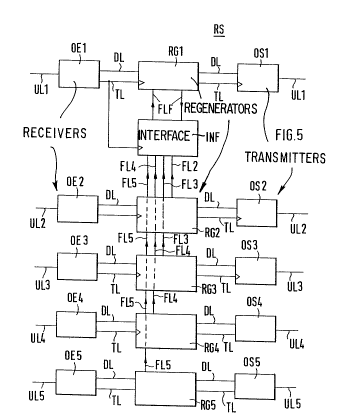
Flgure 5 shows a conf lgurat lon example of a
regeneratlon statlon RS wlth flve transmlss$on llnes ULl to
UL5. Each transmlsslon llne ULl to UL5 ls equlpped wlth a
recelver OEl to OE5, a regenerator RGl to RG5 and a
transmltter OSl to OS5. In the lllustrated regenerators RG2
to RG5, the pertlnent transmlsslon error detectlons UE are not
shown separately, but only as pertalnlng to regenerators RG2
to RG5 by thelr error llnes FL2 to FL5. The operatlng mode of
regenerators RG2 to RG5 was already descrlbed ln the
conf lgurat lon example of f lgure 1.
Regenerator RGl represents a known regenerator,
whlch complles wlth CCITT-RPc-- ~ tlon G.958, l.e. lt
contalns a demultlplexer followed by a multlplexer, and
-- 8 --
` ~- 72430-180
_ _ _ , .. ... . .. . .. .... . ... .
206300 1
between them a circuit for inserting bits into the parity byte
~31, in case ~TM-4 si~nals or si~nals of a higher
multipllcatlon step are transmltted, 80 that the transmlsslon
error probablllty can be detected by parlty determlnatlon.
This means that bits can be inserted lnto the head part ~OH of
regenerator RGl.
- 8a -
72430-180
~,,, ,~
2 ~) 6 3 0 0 1 902-089
Fu lil ll - lr the service chaMel in _ - RG1 can also be used,
which means that byte F1, or others intended for national use for example, or still
unfilled bytes, can be used.
Thus, ~ r RG1 is able to transmit "inband" the i error
S probability, which was determined by ~ - RG2 to RGS, to the head part
of an STM~ signal. To that effect, error lines FL2 to FLS are coMected to an
interface INF, through which the ~ - error probability is inserted into
service channel F1 by error line F~F.
The insertion then conforms to the CCITT~ , and is
10 known as such.
Interface INF is timed by a timing line TL, which is connected to receiver
O~il. Special ~ i.4ti~ between RG2 to RGS and interface
INF is not required, because i through the error line takes place at a
:-. rate of only 8 ~Iz, or a fraction thereof. Interface INF compiles the
~ . error probability in the individual v RG2 to RGS in
specific form, so that central unit Z can determine which ~ ." error proba-
bili!y belongs to what O section. To that effect, the error signal inserted
into service chaMel F1 may contain a code for the 'iv section and a
number to identify the l ~ n line UL2 to ULS. The error signals in error
20 lines FLF can be transmitted in series as block error numbers.
Figure 6 depicts the last three 1~6~ .,dL.,. stations RSN-I, RSN-2 and
RSN l~~ i..g all . v stations of one i - - segment and central
unit Z. T~ f~ll lines ULM connect the lv6~ d~v. stations RSN... to each
other and to central unit Z. Such a i segment may have up to 50
v stations RS, where the sections between the ~ f stations RSN
represent ll6~ dtlvl sections that are individually controlled for i
error monitoring of each i line UL.
,~ o ~ 3 0 0 1 902-089
If a problem or ;, ~ ;.... of a ~ Iine occurs, the transmis-
sion error probability determined in each ~ unit RE in oentral unit Z can
indicate the 1~ .1fLLVI section in which the problem or .: occurred. By
- contrast to - g,~- RGl, which comply with CCITT-R ' G.958 by i error moni~r~no, in which the B1-byte always determines the
error probability between two _ stations, the ~,
unit RE according to the invention determines the ~ error probability
with respect to only one data souroe, thus it increases from .-,6~ lul station to
station. In tbis case, when ~ problem messages, the thresh
10 old from ll _ station to IL~. ll~dlvl station must be increased. To limit
this absolute ~ error probability, in one cnnfi,ol~fi~n example, the
word or words used to determine the i error probability are ~v~- d
in each fifth ~ unit that complies with CClTT n~, ' " G.958.
To that effect, the l'C~,..II..ldl(JI unit RG1, which complies with CCITT-ref f.dation, G.958, is cyclically il~t. ~ L,.il in each following ~c unit RS
with the, _ units RG2 to RG5 of the in~ention, so that each ~
line ULN, N = l, 2, 3, 4, 5 contains a sequence of four 1. g. ~ units
according to the invention, and which comply with CClTT-R~f.~ ;f~l
G.958. Of course, the ~ lif .,~ between " units complying with
CCITT-~f~f~ inn G.958, and tne ,~ units according to the inven
tion, can be varied as needed for each ~ line ULN. The number S used
as tlle number of ~ ;,- - - - lines only represents an example, it may be largeror smaller.
Figure 7 depicts a i segment, in which error line FL is not
connected to central unit Z by an STM~ signal, but by an additional extemal lineFLZ. This cnnfiell~tif)n suggests itself when only l~v ~ RG according to
, . .
902-089
2a6300 1
the invention are located in the -,6~.~.,AIur stations RSN, or the "inband" trans-
mission is not ~1~,~6~ for other reasons
A network junction point, an end point or even a network manager
provided for the ~J~ ullu~l~ digiti~l i may represent a central unit Z.
5 In the case of the r. nnfieu~fir~n example in Figure 7, any desired device could be
viewed as a central unit Z which is capable of describing thc inband and which
can insert the ~ error probability into the head part of an STM-N
signal.
The ,~".r~ .... examples refer to optical; systems.
10 Selecting other or receivers makes it possible to use the invention also
for radio or electrical line I I A~
By contrast to known v that comply with CClTT-Recommen-
dation G.958, the advantage of the, r~rl ,. ., ~ " ~ RG of the invention is in the lack
of ~ ; 7 such as the l~ PII~A~ d~ or the ~ I.Iy for
15 ~ e parity, and the SUbA~ IIblY required to insert the parity into the head
part of an STM-N signal. In that rln the l~ < RG ûf f~e invention
re~uire cr n~ hly less energy, which reduces their cooling cost. The low
energy l~ u.ic--~ has special meaning for opti~al ~ sections, for
example when these are installed in U r ~ ' ' ` areas, and the le6~n~,.dt~i stations
20 RS mus~ be supplied with locally produced current, e.g. by solar cells.
The ,~..,ri~"...li..., examples only refer to the i of datd in one
direction. For two-directional I I A~ , each of the ~., stations RS
have two l~.g~.ll~a~UI units RE, one for 1,.~ in one direction, and the
other for ~ A'~ in the opposite direction. The 1~6~ UI station R~i for
l~ e in one direction can only contain 1~6~ .dtui units RE according to
the invention, who~e error lines FL are connected to a ~ ,d~Ol unit for the
11
902-089
206300 i
opposite direction, which complies with CClTI-r' ' G.958, through
an interface for inband ~
12
s