Note: Descriptions are shown in the official language in which they were submitted.
-
WHITE LEVEL DETECTION CIRCUIT 3 o 7 o
FOR AN OPTICAL IMAGE READER ~U
BACKGROUND OF THE INVENTION
1. Field of the Invention
S The present invention relates to a white
level detection circuit for an optical image
reader, such as an optical character reader (OCR),
a bar code reader or an image scanner.
2. Description of the Prior Art
An optical image reader is known which
optically reads an image by using opto-electric
transducing elements, such as image sensors and
photo diodes, and processes image data generated
by those elements. An optical character reader
(OCR) and a bar code reader are examples of this
type of optical image reader. An image signal
output from an image sensor is converted into
binary image data. The binary image data is
processed for recognizing characters and bar
codes. It is common practice that image data is
processed on the basis of a white level (signal
level) corresponding to a background portion of
high value (e.g., white color) in the image.
The white level may not be uniform over
the image for various reasons, such as
nonuniformity of an illuminating light source,
deterioration of the efficiency of an imaging lens
around the fringe of the image by the cos4 rule,
the quality of paper bearing the image data and
dirt on the surface of the paper. To accurately
reproduce an image, it is necessary to accurately
know the white level, which varies with location,
on the image.
A basic construction of a white level
detection circuit thus far employed in a bar code
reader, for example, is shown in Fig. 4. The
white level detection circuit is essentially a 7
peak hold circuit. An output signal of an image
sensor constituting an input image signal is
applied through a buffer amplifier 1 and a diode 2
to a capacitor 3. The capacitor 3 is charged with
the image signal, and discharged through a
resistor 4. A potential appearing at the terminal
of the capacitor 3 provides a white level signal,
by way of a buffer amplifier 5.
Fig. 5 is a diagram showing a waveform
useful in explaining the operation of the white
level detection circuit of Figure 4. The image
signal is represented by a curve L1, and the white
level signal by a curve L2. Consider the simple
case of a black bar code formed on white paper. A
white period W corresponds to a white portion in
the image, and a black period B, to a black
portion (i.e., black bar). A period TB indicates
a blank period of the image sensor. When the
image signal increases, the capacitor 3 is charged
through the diode 2. When the image signal
decreases, the capacitor 3 is discharged at a
preset time constant, through the resistor 4.
When a point being read changes from black to
white, the image signal sharply rises and
capacitor 3 charges through the diode 2. As a
result, during the white period W, a white level
signal, equal to the image signal, is output.
When the point being read changes from black to
white, the image signal sharply falls. Capacitor
3 discharges thereby maintaining the image signal
substantially equal to the value during the
previous white period W. Changes in the white
level, which are due to changes of value or
brightness in the white portion on the paper, are
subtle. Accordingly, when the white level on the
2063070
paper falls, the white level signal accurately
follows the fall of the white level.
In the prior art, if a relatively long
black portion exists, a long black period BL
appears, as shown in Fig. 6. In this situation,
the discharge of the capacitor 3 is completed by
the end of the long black period BL. The white
level signal (indicated by curve L2) falls to
approach to the level of the image signal
corresponding to the black portion as shown by
reference character al. When the image signal is
processed on the basis of such a white level
signal, the black portion may be mistakenly
recognized as the white portion. Although a
mistake in recognition in which the white portion
is recognized as the black portion or vice versa
would never occur, the image signal of the black
portion is increased in comparison to the white
level signal, resulting in distortion of the
recognized image. The distortion adversely
affects the bar code discriminating processing,
which includes binary processing.
One approach to solving this problem
would be to sufficiently increase the discharge
time-constant defined by the capacitor 3 and the
resistor 4. This approach, however, may result in
the failure of the white level signal to follow
the natural fall of the white level on paper.
An arrangement which solved the problem
of distorted images, is shown in Fig. 7. The
arrangement includes a peak hold circuit 11 which
has a variable discharge time-constant. The
discharge time constant of the peak hold circuit
11 is selectively changed by a switch circuit 12
which selects a short time constant for the white
portion and a long time constant for the black
portion. The peak hold circuit 11 includes a
2063070
capacitor, a diode for charging the capacitor, and
a resistor for discharging the capacitor.
An image signal is applied to peak hold
circuit 11 and to differentiation circuit 13. A
derivative or differential coefficient produced by
differentiation circuit 13 is compared to proper
threshold levels TH1 and TH2 (TH1 > 0 > TH2) in
comparator circuit 14. The output signal of
comparator circuit 14 is applied to flip-flop 15
as either set signal S or reset signal R, thereby
controlling switch circuit 12. Switch circuit 12
is rendered conductive or nonconductive depending
on the state of flip-flop 15, thereby selecting
the discharge time constant of the peak hold
circuit 11 to be either short or long,
respectively.
Figs. 8(a) through 8(d) are diagrams
showing waveforms useful in explaining the
operation of the prior art circuit of Fig. 7.
Fig. 8(a) shows an image signal waveform. Fig.
8(b) shows a waveform of the corresponding output
signal of differentiation circuit 13. Fig. 8(c)
shows a waveform of the resulting output signal of
flip-flop 15. Fig. 8(d) shows the resultant
output waveform of white level signal from peak
hold circuit 11.
The image signal changes sharply at the
start and end points of blank period TB and black
period B. Pulse signals having polarity based on
changes in the image signal, are output from
differentiation circuit 13. When the signal is
processed from blank period TB to white period W,
and from black period B to white period W, the
output signal of differentiation circuit 13
becomes a large positive signal, exceeding
threshold level THl. As a result, the comparator
circuit 14 produces a set signal S, setting the
2063û70
flip-flop 15, which in turn produces an output
signal of logic "1". Consequently, switch circuit
12 selects a short discharge time constant of peak
hold circuit 11. Accordingly, during period W,
the white level signal accurately follows the
change of the image signal.
When the signal is processed from white
period W to either blank period TB or black period
B, the output signal of diferentiation circuit 13
is negative in polarity, falling below threshold
value TH2. As a result, reset signal R is derived
from comparator circuit 14, and resets the flip-
flop 15 which in turn produces an output signal of
logic "O". In response, switch circuit 12 selects
lS a large discharge time-constant of the peak hold
circuit 11. As a result, even if black period B
is long, the white level signal can substantially
maintain its value from the end of the previous
white period. Accordingly, the black portion will
not be mistaken for the white portion because the
image distortion caused when the image signal in
the black portion increases relative to the white
level signal has been eliminated.
However, this prior art is not problem-
free. When the white level on the paper surfacefalls during a long black period B, a proper white
level signal cannot be obtained during the
subsequent white period. This problem will be
further described below with respect to Figures
9(a) and 9(b).
If, as shown in Fig. 9(a), the white
level on the read surface increases by ~wl during
the long black period BL1, peak hold circuit 11
immediately increases the white level signal which
follows the image signal variation, during the
white period W following the black period BL1. To
the contrary, if as shown in Fig. 9(b), the white
2063070
- level on the read surface decreases by ~w2 during
the long black period BL2, peak hold circuit 11
cannot immediately follow a variation of the
decreased image signal during the white period W
after the black period BL2. Rather, it slowly
follows the variation of the decreased image
signal at a time constant. As a result, during
the white period W following black period BL2, a
white level signal which is higher than the actual
white level is output because image signal input
during the white period W after the black period
BL2 is lower than the white level signal retained
in peak hold circuit 11 and cannot actively charge
the capacitor in peak hold circuit 11. In other
words, the circuit, out of necessity, waits until
completion of the discharge of the capacitor with
a time constant, in order that the white level
signal changes after the image signal changes.
Otherwise, when the white level signal is improper
during the white period W, the white image is
distorted.
A similar problem also arises when the
white level of the image changes at the start
point and the end point of the image scanning
period. When the white level of the image signal
at the start point of the scan period is higher
than the white level at the end point by ~w, as
shown in Fig. 10, the white level signal retained
during blank period TB cannot immediately follow
the image signal variation in the leading portion
of the white period subsequent to blank period TB.
As a result, as in the above case, the image in
the white portion is distorted.
Accordingly, an object of the present
invention is to provide a white level detection
circuit for an optical image reader which produces
a white level signal that accurately follows a
2063070
- variation of the white level on the surface, and
produces a white level signal that allows for
excellent processing of the image signal
corresponding to the black portion.
S SUMMARY OF THE INVENTION
A white level detection circuit is used
for an optical image reader in which light
reflected from a read surface is converted into an
electrical image signal by opto-electric
transducing means, and the image is read on the
basis of the resulting image signal. The white
level is detected as the image signal level
corresponding to a background portion of high
value in the image. The white level detection
circuit comprises a sample/hold means for
receiving the image signal from the opto-electric
transducing means and then producing a white level
output signal. The operation mode of the
sample/hold means is switched, in response to an
external control signal between a sample mode in
which the sample/hold means produces a signal
following a variation of the image signal, and a
hold mode in which the sample/hold means produces
a signal at a fixed level corresponding to the
image signal level of the previous sample mode.
The detection circuit also comprises a control
means for generating a control signal which places
the sample/hold means in the sample mode when the
opto-electric transducing means output signal
greatly increases or the hold mode when the opto-
electric transducing means output signal greatly
decreases.
When a point on the read surface shifts
from an image portion of low value to a background
portion of high value, the output signal of the
opto-electric transducing means sharply increases.
2063070
- In response, the sample/hold means is placed in a
sample mode. In the sample mode, the sample/hold
means produces a signal (e.g., an image signal per
se) following a variation of an image signal in
the form of a white level signal. Accordingly, it
generates an accurate white level signal
corresponding to the background portion when the
image signal either rises or falls. Thus, the
processing of the image signal of the background
portion based on the white level signal, can be
accurately performed.
When a point shifts from a background
portion of high value to an image portion of low
value, the output signal of the opto-electric
transducing means sharply decreases. In response,
the sample/hold means is placed in a hold mode.
In the hold mode, the white level signal held
remains unchanged in level over the entire period
of the hold mode. Therefore, even when the image
portion of low value persists, the white level
signal remains unchanged. The signal corresponding
to the image portion of low value can be processed
while remaining free from image distortion.
The sample/hold means can accurately
follow a continuous variation of the image signal,
but it does not follow a discontinuous or
extremely steep variation of the image signal
detected by the differentiation circuit.
Therefore, depending on the sharp increase or the
sharp decrease of the image signal, the white
level changes with the image signal. Thus, when
no image signal is present, and the image signal
comes in and first rises, the white level is
incorrect for an instant, but it follows the image
signal level in the sample mode during one scan
operation, and once the white level is corrected,
it accurately follows the image signal level
2063070
variation. Therefore, the instantaneous incorrect
white level state is negligible in practical use.
In the white level detection circuit of
another embodiment, the control means includes a
differentiating means for detecting a derivative
of the opto-electric transducing means output
signal, a comparing means for comparing the
- differentiating means output signal with a
positive first threshold level and a negative
second threshold level, respectively. The
comparing means produces a set signal when the
output signal of the differentiating means exceeds
the first threshold level, and a reset signal when
the output signal of the differentiating means
falls below the second threshold level. The
control means also comprises a hold means for
placing the sample/hold means in the sample mode
in response to the set signal from the comparing
means, and for placing the sample/hold means in
the hold mode in response to the reset signal from
the comparing means.
Therefore, the differentiating means can
detect a sharp increase or a sharp decrease of the
image signal. The comparing means compares a
derivative of the image signal output from the
differentiating means with the first or the second
threshold level. The increase or decrease of the
image signal is determined during the comparing
operation. The first threshold level takes a
positive value. The derivative, when it exceeds
the first threshold level, indicates the steep
increase of the image signal. Subsequent to the
increase of the image signal, the point to be read
is present in the background portion of high
value. At this time, the comparing means produces
a set signal. In response to the set signal, the
hold means outputs and holds a control signal
-
- placing the sample/hold means in a sample mode 2 0 6 3 0 7 0 which then produces a white level signal following
the image signal for the background portion of
high value.
The second threshold level takes a
negative value. The derivative detected by the
differentiating means, when it falls below the
second threshold level, indicates the steep
decrease of the image signal. Subsequent to the
image signal decrease, the point to be read is
present in the image portion of low value. At
this time, the comparing means produces a reset
signal, and the hold means outputs and holds a
control signal placing the sample/hold means in a
hold mode for the low value image portion.
BRIEF DESCRIPTION OF THE DRAWINGS
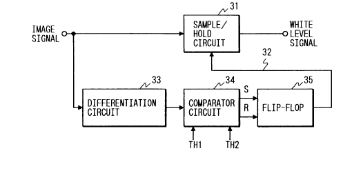
Fig. 1 is a block diagram showing the
basic arrangement of a white level detection
circuit for an optical image reader according to a
preferred embodiment of the present invention.
Fig. 2 is a circuit diagram showing the
detailed arrangement of the white level detection
circuit.
Fig. 3 is a timing chart useful in
explaining the operation of the white level
detection circuit.
Fig. 4 is a circuit diagram showing the
basic construction of a conventional white level
detection circuit.
Fig. 5 is a diagram showing a waveform
useful in explaining the operation of the white
level detection circuit thus arranged.-
Fig. 6 is a diagram showing a waveform
for explaining the problem of the prior art white
level detection circuit.
-- 10 --
2063070
Fig. 7 is a block diagram showing prior
art.
Fig. 8 is a diagram showing a set of
waveforms useful in explaining the operation of
the prior art circuit.
Fig. 9 is a waveform diagram for
explaining a problem of the prior art.
Fig. 10 is a waveform diagram for
explaining another problem of the prior art.
DESCRIPTION OF THE PREFERRED EMBODIMENT
A preferred embodiment of the present
invention will described with reference to the
accompanying drawings.
Fig. 1 is a block diagram showing the
basic arrangement of a white level detection
circuit for an optical image reader according to a
preferred embodiment of the present invention.
The white level detection circuit is used for an
optical image readers, such as a bar code reader
or an optical character reader. Optical image
readers are, in turn, used for reading images on
white paper surfaces, upon which black bar codes
and characters are formed. The white level
detection circuit detects the image signal which
corresponds to the white portion of the surface as
the background and is read in the form of a white
level. The image signal is obtained, when the
paper surface is illuminated with light and the
reflected light is converted into an electrical
signal by an opto-electric transducing element, an
example of which comprises an image sensor and
photo diodes.
An image signal derived from the opto-
electric transducing element is applied to
sample/hold circuit 31. Under control of a
control signal from line 32, the sample/hold
2063070
._
circuit 31 is operable in either of two modes: a
sample mode in which it produces a signal
following an image signal variation or a hold mode
in which it holds, i.e., maintains, the signal
level from the previous sample mode. The output
image signal of sample/hold circuit 31 is used as
a white level signal. The binary processing of
the image signal and the discriminating processing
for characters and bar codes are performed on the
basis of the white level signal.
The image signal from the opto-electric
transducing element is also applied to
differentiation circuit 33 for detecting the
derivative or differential coefficient of the
image signal. Differentiation circuit 33 produces
a positive signal when it receives the leading
edge of the image signal, and a negative signal
when it receives the trailing edge. The amplitude
of the differentiation circuit output signal
depends on the rate of change of the image signal.
The output signal of differentiation
circuit 33 is applied to comparator circuit 34
where it is compared with a positive first
threshold level THl and a negative second
threshold level TH2 (TH1 > 0 > TH2), respectively.
When the output signal of differentiation circuit
33 is higher than the first threshold TH1, the
comparator circuit 34 produces a set signal S.
When it is lower than the second threshold level
TH2, the circuit produces a reset signal R.
The set signal S and the reset signal R
output from comparator circuit 34 are applied to
RS (set/reset)-flip-flop 35. Flip-flop 35 is set
by the set signal S from comparator circuit 34,
and transmits a signal logic "1" onto the line 32.
The flip-flop is reset by the reset signal R, and
transmits a signal logic "0" onto the line 32.
2063070
The signal from the flip-flop 35 is
applied as a control signal to sample/hold circuit
31. When the logic "l" signal is derived onto the
line 32, sample/hold circuit 31 is placed in the
sample mode. When the logic "0" signal is derived
onto the line 32, sample/hold circuit 31 is placed
in the hold mode. Differentiation circuit 33,
comparator circuit 34, and flip-flop 35 make up a
control means for the detection circuit.
Fig. 2 is a circuit diagram showing a
detailed arrangement of the white level detection
circuit according to a preferred embodiment of the
present invention.
Sample/hold circuit 31 is made up of
input buffer 41, analog switch 42 for switching an
image signal applied through input buffer 41,
capacitor 43 for holding the signal applied
through analog switch 42, and output buffer 44. A
potential appearing at the terminal of capacitor
43, which is connected to analog switch 42, is
derived as a white level signal through output
buffer 44. The control signal from the line 32 is
connected to the gate of analog switch 42.
Through the switching operation of analog switch
42, the operation of the sample/hold circuit 31
can be switched from the sample mode to the hold
mode, or vice versa.
When analog switch 42 is conductive, the
signal derived from output buffer 44 corresponds
directly to the image signal, and, accordingly,
the sample mode is set up. When analog switch 42
is nonconductive, the signal applied through
analog switch 42 is held in capacitor-43
immediately before the switch is turned off, and
the hold mode is set up.
Differentiation circuit 33 consists of
capacitor 45 and resistor 46. When the output
2063070
impedance of the pre-stage of differentiation
circuit 33 is high, an input buffer is preferably
provided at the input of the differentiation
circuit.
Comparator circuit 34 includes
comparators 51 and 52. The inverting input
terminal of comparator 51 receives the first
threshold level TH1, and the noninverting input
terminal thereof receives an output signal of
differentiation circuit 33. A high level signal
output from comparator 51 serves as the set
signal. The comparator 52 receives the output
signal of the differentiation circuit 33 at the
inverting input terminal, and the second threshold
level TH2 at the noninverting input terminal. The
high level signal output from comparator 52 serves
as the reset signal R. The output signal of
comparator 51 is applied to the set input terminal
35s of flip-flop 35. The output signal of
comparator 52 is applied to the reset input
terminal 35r of flip-flop 35. If flip-flop 35 is
constructed with two NAND gates, as the case may
be, the input of the flip-flop must be the
negative logic signal "0".
Figs. 3(a) through 3(g) are timing charts
useful in explaining the operation of the white
level detection circuit thus arranged. Fig. 3(a)
shows an image signal waveform output signal of an
opto-electric transducing element. Fig. 3(b)
shows a waveform of an output signal of
differentiation circuit 33. Fig. 3(c) shows a
waveform of a set signal S output from comparator
circuit 34. Fig. 3(d) shows a waveform of a reset
signal R output from comparator circuit 34. Fig.
3(e) shows a waveform of a signal derived from
flip-flop 35 and applied to the line 32. Fig.
3(f) shows a variation in the state of sample/hold
- 14 -
2063070
circuit 31. Fig. 3(g) shows a waveform of a white
level signal output from sample/hold circuit 31.
During the white periods W1 and W2, which
correspond to white portions which serve as the
background of an image, the image signal is
relatively large. During the black period B
corresponding to the black portion of the surface,
the image signal is relatively low, and during the
blank period TB of one scan period, the image
signal takes the minimum value. "One scan period"
means a period taken for electrically scanning a
line, or row, of elements such as when an image is
read by using a 2-dimensional image sensor. When
an image is scanned with a laser beam and light
reflected from the surface is detected by a photo
diode, the "one scan period" refers to a period
taken for the laser beam to scan one image.
The output signal of differentiation
circuit 33, which is the derivative of the image
signal, takes a large value as indicated by bl in
connection with a steep increase in the image
signal when the point to be read is moved from the
blank period TB to the white period W1. When the
large value exceeds the first threshold level TH1
in comparator circuit 34, comparator 51 outputs a
high logic level (set signal S). With the high
level signal, flip-flop 35 is set, so that a
signal logic "1" is transmitted to the line 32.
In sample/hold circuit 31, analog switch 42
becomes conductive to place sample/hold circuit 31
in the sample mode. As indicated by b2 in Fig.
3(g), the white level signal exhibits a variation
resembling the image signal. In the sample mode,
the white level signal follows the variation of
the image signal without any delay.
In the transition from the white period
Wl to the black period B and from the white period
-
-
2063070
W2 to the blank period TB, the image signal
sharply decreases as indicated by b3 and b4 in
Fig. 3(a). At this time, the output signal of
differentiation circuit 33 has a large magnitude
and a negative polarity. The values of the output
signal, denoted as b5 and b6 in Fig. 3(b), are in
excess of the second threshold level TH2. As a
result, the flip-flop 35 is reset, so that a
signal of logic "0" is transmitted to the line 32.
The logic "0" signal turns off analog switch 42 in
sample/hold circuit 31, to prohibit the image
signal from being input. Consequently, the white
level signal is held at the signal level retained
in the capacitor 43, that is, the signal level
(denoted as b7 in Fig. 3(g)) at the end of the
previous white period W1. Thus, the image signal
processing during the black period B is accurately
performed on the basis of the suitable white level
signal. Even when the black period B is long, the
white level signal remains unchanged, and hence,
there is no distortion in the black portion of the
image.
Next, operation when the read point is
moved from the black period B to the white period
W2 is described. In the transition, the sharp
increase in the image signal is indicated by b8 in
Fig. 3(a). When the output signal of
differentiation circuit 33 exceeds the first
threshold level THl, a set signal S is derived
from the comparator circuit 34, thereby placing
sample/hold circuit 31 in the sample mode. If the
image signal is higher than the potential retained
in capacitor 43, capacitor 43 is quickly charged.
But if the image signal is lower than capacitor
43, capacitor 43 is quickly discharged. Figs.
3(a) through 3(g) show a case where the image
signal during the white period W2 which follows
- 16 -
2063070
the black period B is smaller than the image
signal at the end of the white period Wl which
precedes the black period B. In such a case, the
white level signal quickly follows the value
S corresponding to the image signal, as indicated by
b9 in Fig. 3(g).
The operation is similarly performed in
the transition from the blank period TB to the
white period W1. Even when the white level in the
initial part of the scan range is different than
in the end part thereof, an excellent white level
signal may be generated in the respective parts.
As described above, in the present
embodiment, a white level signal corresponding to
the white portion preceding to the black portion,
can be produced for the black image portion.
Accordingly, the image signal corresponding to the
black portion may be well processed. Even if the
white level of the white portion that follows the
black portion is lower than the white level of the
white portion that was read before the black
portion, the white level detection circuit can
produce a white level signal accurately following
such a low white level. Therefore, the image
signal corresponding to the white portion may also
be well processed.
In this way, the image signals of both
the white and black portions may be processed in a
satisfactory manner, thereby improving the
performance of reading characters, bar codes,
symbols, and other images.
It should be understood that the present
invention is not limited to the embodi-ment as
mentioned above, but may be variously modified,
changed and altered within the spirit and the
scope of the appended claims.