Note: Claims are shown in the official language in which they were submitted.
The embodiments of the invention in which an
exclusive property or privilege is claimed are defined as
follows:
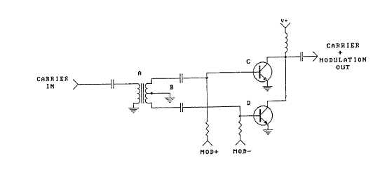
1. A BPSK Modulator circuit, comprising:
a transformer, said transformer further comprising
first induction means having a carrier input leg and an
output leg, second induction means having first and second
leg outputs, said transformer configured such that said
first and second leg outputs of said second induction means
modulates at opposite phases of 180 and 0 degrees, forming
"MOD +" and "MOD -", respectively, relative a carrier
signal supplied to said carrier input of said first
induction means;
first and second phase selection means configured to
modulate via input of said first and second outputs of said
second induction means, said first and second phase
selection means further comprising first and second load
transistors or their equivalent, respectively, each having
an emitter, and a base or the equivalent, said base of said
first transistor in circuit with said first output of said
second inductor, receiving said "MOD +" , said base of said
second transistor in circuit with said second output of
said second inductor, receiving said "MOD -".
2. A BPSK Modulator circuit having a tunable slug or
core to adjust carrier suppression in a spread spectrum
system, comprising:
a transformer, said transformer further comprising
first induction means having a carrier input leg and an
output leg, second induction means having first and second
leg outputs, and a tunable slug or core in communication
with said first and second induction means, said
transformer configured such that said first and second leg
outputs of said second induction means modulates at
opposite phases of 180 and 0 degrees, forming "MOD +" and
"MOD -", respectively, relative a carrier signal supplied
to said carrier input of said first induction means;
first and second phase selection means configured to
modulate via input of said first and second leg outputs of
said second induction means, said first and second phase
selection means further comprising first and second load
transistors, respectively, each having an emitter, a
collector, and a base, said base of said first transistor
in circuit with said first output leg of said second
inductor, receiving said "MOD +", said base of said second
transistor in circuit with said second output leg of said
second inductor, receiving said "MOD -".
3. A BPSK Modulator circuit utilizing a loosely coupled
transformer to adjust carrier suppression in a spread
spectrum system, comprising:
a transformer, said transformer further comprising
first induction means having a carrier input leg and an
output leg, second induction means loosely coupled with
said first induction means, said second induction means
having first and second leg output, said transformer
configured such that said first and second leg outputs of
said second induction means modulates at opposite phases of
180 and 0 degrees, forming "MOD +" and "MOD -",
respectively, relative a carrier signal supplied to said
carrier input of said first induction means;
first and second capacitors, said first capacitor in
parallel circuit with said carrier input leg and grounded
output leg of said first induction means, said second
capacitor in parallel circuit with said first and second
leg outputs of said second induction means, first and
second phase selection means configured to modulate via
input of said first and second outputs of said second
induction means, said first and second phase selection
means further comprising first and second load transistors,
respectively, each having an emitter, a collector, and a
base, said base of said first transistor in serial circuit
with said first leg output of said second inductor,
receiving said "MOD +", said base of said second transistor
in serial circuit with said second leg output of said
second inductor, receiving said "MOD -".
4. The BPSK Modulation System of claim 3, wherein there
is further included a tunable slug or core in communication
with said first and second inductors.
5. The BPSK Modulation System of claim 4, wherein there
is further included resonator capacitor means in parallel
circuit with said first and said second leg outputs of said
second induction means, said resonator capacitor
transformer coupling means configured to provide band pass
filtering for previous stage harmonic suppression.
6. A BPSK Modulator circuit having a tightly coupled
transformer having no center tap and a single parallel
resonate capacitor on the secondary to provide BPSK
modulation, comprising:
a transformer, said transformer further
comprising first induction means having a carrier input leg
and an output leg, second induction means tightly coupled
to said first induction means, said second induction means
having first and second leg outputs, said transformer
configured such that said first and second leg outputs of
said second induction means modulates at opposite phases of
180 and 0 degrees, forming "MOD +" and "MOD -",
respectively, relative a carrier signal supplied to said
carrier input of said first induction means;
band pass filter means for filtering harmonic
suppression from said transformer, said band pass filter
means further comprising a resonate capacitor in parallel
circuit with said first and second leg outputs of said
second induction means;
first and second phase selection means configured to
modulate via input of said first and second outputs of said
second induction means, said first and second phase
selection means further comprising first and second load
transistors, respectively, each having an emitter, a
collector, and a base, said base of said first transistor
in circuit with said first leg output of said second
inductor, receiving said "MOD +", said base of said second
transistor in circuit with said second output of said
second inductor, receiving said "MOD -".
7. The BPSK Modulation System of claim 6, wherein said
system further comprises adjustment means for adjusting
carrier suppression, said adjustment means further
comprising a tunable slug or core in communication with
said first and second induction means.
8. The BPSK Modulation System of claim 6, wherein there
is further included resonator capacitor means in parallel
circuit with said first and said second leg outputs of said
second induction means, said resonator capacitor means
configured to provide band pass filtering for previous
stage harmonic suppression.
9. The BPSK modulation System as set forth in claim 3,
further including a fixed transformer and a variable tuning
capacitor, said fixed transformer in communication with
said first and second induction means.
10. The BPSK modulation system as set forth in claim 6,
further comprising adjustment means for adjusting carrier
suppression, said adjustment means including a fixed
transformer and a variable tuning capacitor, said fixed
transformer in communication with said first and second
induction means.
11. A frequency multiplier circuit utilizing a loosely
coupled transformer to adjust carrier suppression,
comprising:
a transformer, said transformer further comprising
first induction means having a carrier input leg and an
output leg, second induction means loosely coupled with
said first induction means, said second induction means
having first and second leg output, said transformer
configured such that said first and second leg outputs of
said second induction means modulates at opposite phases of
180 and 0 degrees, forming "MOD +" and "MOD -",
respectively, relative a carrier signal supplied to said
carrier input of said first induction means;
first and second capacitors, said first capacitor in
parallel circuit with said carrier input leg and grounded
output leg of said first induction means, said second
capacitor in parallel circuit with said first and second
leg outputs of said second induction means,
phase selection means configured to modulate via
input of said first and second outputs of said second
induction means, said phase selection means having a F t > 1
GHz, and further comprising an emitter, and first and
second bases or the equivalent, said first base in circuit
with said first output of said second inductor, receiving
said "MOD +", said second base in circuit with said second
output of said second inductor, receiving said "MOD -".
12. A frequency multiplier circuit, comprising:
a transformer, said transformer further comprising
first induction means having a carrier input leg and an
output leg, second induction means having first and second
leg outputs, said transformer configured such that said
first and second leg outputs of said second induction means
modulate at opposite phases of 180 degrees and 0 degrees,
forming "MOD +" and "MOD -", respectively, relative to a
carrier signal supplied to said carrier input of said first
induction means; and
phase selection means configured to modulate via
input of said first and second outputs of said second
induction means, said phase selection means having a F t > 1
GHz, and further comprising an emitter, and first and
second bases or the equivalent, said first base in circuit
with said first leg output of said second induction means,
receiving said "MOD +", said second base in circuit with
said second leg output of said second induction means,
receiving said "MOD -".
13. A frequency multiplier circuit utilizing a loosely
coupled transformer to adjust carrier suppression,
comprising:
a transformer, said transformer further comprising
first induction means having a carrier input leg and an
output leg, second induction means loosely coupled with
said first induction means, said second induction means
having first and second leg outputs, said transformer
configured such that said first and second leg outputs of
said second induction means modulate at opposite phases of
180 degrees and 0 degrees, forming "MOD +" and "MOD -",
respectively, relative to a carrier signal supplied to said
carrier input of said first induction means;
first and second capacitors, said first capacitor in
parallel circuit with said first and second leg outputs of
said second induction means; and
phase selection means configured to modulate via
input of said first and second outputs of said second
induction. means, said phase selection means having a F t > 1
GHz, and further comprising an emitter, and first and
second bases or the equivalent, said first base in circuit
with said first output of said second induction means,
receiving said "MOD +", said second base in circuit with
said second output of said second induction means,
receiving said "MOD -".
14. A BPSK Modulator circuit having a fixed transformer
and a variable tuning capacitor, the fixed transformer and
variable tuning capacitor to adjust carrier suppression in
a spread spectrum system, comprising:
a transformer, said transformer further comprising
first induction means having a carrier input leg and an
output leg, second induction means having first and second
leg outputs, a fixed transformer, and a variable tuning
capacitor, the fixed transformer in communication with said
first and second induction means, said transformer
configured such that said first and second leg outputs of
said second induction means modulate at opposite phases of
180 degrees and 0 degrees, forming "MOD +" and "MOD -",
respectively, relative to a carrier signal supplied to said
carrier input of said first induction means; and
first and second phase selection means configured to
modulate via input of said first and second outputs of said
second induction means, said first and second phase
selection means further comprising first and second load
transistors, respectively, each having an emitter, a
collector, and a base, said base of said first transistor
in circuit with said first output leg of said second
induction means, receiving said "MOD +", said base of said
second transistor in circuit with said second output of
said second induction means, receiving said "MOD -".
15. The method of modulating a carrier between a 0
degree phase shift and a 180 degree phase shift, comprising
the following steps:
a. providing a transformer, said transformer
further comprising first induction means having a carrier
input leg and an output leg, and second induction means
having first and second leg outputs, and a tunable slug or
core in communication with said first and second induction
means;
b. tuning said slug or core such that said first
and second leg outputs of said second induction means
modulates at opposite phases of 180 and 0 degrees, forming
"MOD +" and "MOD -", respectively, relative a carrier
signal supplied to said carrier input of said first
induction means;
c. providing first and second phase selection means
configured to modulate via input of said first and second
leg outputs of said second induction means, said first and
second phase selection means further comprising first and
second load transistors, respectively, each having an
emitter, a collector, and a base;
d. configuring said base of said first transistor
in circuit with said first output leg of said second
inductor, receiving said "MOD +", said base of said second
transistor in circuit with said second output leg of said
second inductor, receiving said "MOD -".
16. The method of utilizing a loosely coupled
transformer to adjust carrier suppression, modulating a
carrier signal between a 0 degree phase shift and a 180
degree phase shift, comprising the following steps:
a. providing a transformer, said transformer
further comprising an inductor having first induction means
having a carrier input leg, an output leg, and windings,
and second induction means having first and second leg
outputs and windings;
b. coupling said windings of said first and second
induction means to a >0.6 and <0.3 coupling coefficient;
c. modulating said inductor at opposite phases of
180 and 0 degrees, forming "MOD +" and "MOD -",
respectively, relative a carrier signal supplied to said
carrier input of said first induction means;
d. providing first and second phase selection means
configured to modulate via input of said first and second
leg outputs of said second induction means, said first and
second phase selection means further comprising first and
second load transistors, respectively, each having an
emitter, a collector, and a base;
e. configuring said base of said first transistor
in circuit with said first output leg of said second
inductor, receiving said "MOD +", said base of said second
transistor in circuit with said second output leg of said
second inductor, receiving said "MOD -".
17. The method of claim 16, wherein there is included
the further step of providing first and second capacitors,
said first capacitor in parallel circuit with said carrier
input leg and grounded output leg of said first induction
means, said second capacitor in parallel circuit with said
first and second leg outputs of said second induction
means.
18. The method of multiplying a carrier to provide a
higher frequency harmonic, comprising the following steps:
a. providing a transformer, said transformer
further comprising first induction means having a carrier
input leg and an output leg, and second induction means
having first and second leg outputs, and a tunable slug or
core in communication with said first and second induction
means;
b. tuning said slug or core such that said first
and second leg outputs of said second induction means
modulates at opposite phases of 180 and 0 degrees, forming
"MOD +" and "MOD -", respectively, relative a carrier
signal supplied to said carrier input of said first
induction means;
c. providing phase selection means configured to
modulate via input of said first and second outputs of said
second induction means, said phase selection means having a
F t > 1 GHz, and further comprising an emitter, and first
and second bases or the equivalent, said first base in
circuit with said first output of said second inductor,
receiving said "MOD +", said second base in circuit with
said second output of said second inductor, receiving said
"MOD -"; and
d. configuring said first base in circuit with said
first output leg of said second inductor, receiving said
"MOD +", and said second base in circuit with said second
output leg of said second inductor, receiving said "MOD -",
multiplying the carrier to provide a higher frequency
harmonic.
19. The method of utilizing a loosely coupled
transformer to adjust carrier suppression, modulating
a carrier signal between a 0 degree phase shift and a
180 degree phase shift, and multiplying a carrier to
provide a higher frequency harmonic, comprising the
following steps:
a. providing a transformer, said
transformer further comprising an inductor having
first induction means having a carrier input leg, an
output leg, and windings, and second induction means
having first and second leg outputs and windings;
b. coupling said windings of said first
and second induction means to a >0.6 and <0.3
coupling coefficient;
c. modulating said inductor at opposite
phases of 180 degrees and 0 degrees, forming "MOD +"
and "MOD -", respectively, relative to a carrier
signal supplied to said carrier input of said first
induction means;
d. providing phase selection means
configured to modulate via input of said first and
second outputs of said second induction means, said
phase selection means having a F t > 1 GHz, and
further comprising an emitter, and first and second
bases or the equivalent, said first base in circuit
with said first output of said second inductor,
receiving said "MOD +", said second base in circuit
with said second output of said second inductor,
receiving said "MOD -".
e. configuring said first base in circuit
with said first output leg of said second inductor,
receiving said "MOD +", and said second base in
circuit with said second output leg of said second
inductor, receiving said "MOD -", multiplying the
carrier to provide a higher frequency harmonic.
20. The method of claim 19, wherein there is
included the further step of providing first and
second capacitors, said first capacitor in parallel
circuit with said carrier input leg and grounded
output leg of said first induction
means, said second capacity in parallel circuit with said
first and second leg outputs of said second induction
means.
21. The method of multiplying a carrier to provide a
higher frequency harmonic, comprising the following steps:
a. providing a fixed transformer, said
transformer further comprising first induction means having
a carrier input leg and an output leg, and second induction
means having first and second leg outputs, and a variable
tuning capacitor, said fixed transformer in communication
with said first and second induction means:
b. tuning fixed transformer and variable tuning
capacitor such that said first and second leg outputs of
said second induction means modulates at opposite phases
of 180 degrees and 0 degrees, forming "MOD +" and "MOD -",
respectively, relative a carrier signal supplied to said
carrier input of said first induction means:
c. providing phase selection means configured to
modulate via input of said first and second outputs of said
second induction means, said phase selection means having a
F t > 1 GHz, and further comprising an emitter, and first
and second bases or the equivalent, said first base in
circuit with said first output of said second induction
means, receiving said "MOD +", said second base in circuit
with said second output of said second induction means,
receiving said "MOD -"; and
d. configuring said first base in circuit with said
first output leg of said second induction means, receiving
said "MOD +", and said second base in circuit with said
second output leg of said second induction means, receiving
said "MOD -", multiplying the carrier to provide a higher
frequency harmonic.
22. A method for modulating a carrier frequency signal
by using a transformer to produce a zero degree phase shift
and a 180 degree phase shift of the carrier frequency
signal, said method comprising the steps of:
selectively enabling a zero degree input leg of the
transformer in response to a first binary phase shift
keying (BPSK) signal;
selectively enabling 180 degree input leg of the
transformer in response to a second BPSK signal; and
supplying a carrier signal to the transformer via
said zero degree input leg and said 180 degree input leg,
wherein the zero degree input leg and the 180 degree input
leg are alternately selected by said first and second BPSK
signals to produce BPSK modulation of said carrier
frequency signal at an output of the transformer.
23. The method according to claim 22, wherein the steps
of selectively enabling each include a step of:
biasing a selection means into a linear region of
operation.
24. The method according to claim 22, wherein each of
the steps of selectively enabling each produce a harmonic
of the carrier frequency signal.
25. The method according to claim 24, wherein the steps
of selectively enabling each include a step of:
biasing a selection means to produce a predetermined
harmonic.
26. The method according to claim 22, further comprising
the step of tuning the transformer to a predetermined
output carrier frequency.
27. The method according to claim 26, wherein said step
of tuning is performed using at least one of a capacitor on
a primary winding of the transformer and a capacitor on a
secondary winding of the transformer.
28. The method according to claim 22, further comprising
the step of:
amplifying the carrier frequency signal within each
of said zero degree input leg and said 180 degree input
leg.
29. The method according to claim 22, further comprising
the step of:
loosely coupling and tuning the transformer to a
predetermined output carrier frequency.
30. The method according to claim 22, further comprising
the steg of:
amplifying the selectively enabled carrier signal.
31. The method according to claim 22, wherein the
selection means is enabled to source or sink current.
32. The method according to claim 22, wherein the zero
degree input leg and the 180° input leg are included in a
primary winding of the transformer, said primary winding
having a center tap leg.
33. The method according to claim 22, wherein the steps
of selectively enabling each include a step of:
biasing a selection means into a non-linear region
of operation.