Note: Descriptions are shown in the official language in which they were submitted.
1
PATENT
14?39°1
SNfART SKIN ARRAY WOVEN FIBER OPTIC RIBBON AND ARRAYS
AND PACKAGING THEREOF
BACKGROUND OF THE INVENTION
This invention relates to optical systems and
optical fibers, and particularly to optical fibers woven
into other material to provide sensors or "smart°' skins for
aircraft and other applications.
Fiber optic sensor technology has become
increasingly desirable for monitoring for numerous
applications such as aircraft and spacecraft. The size,
weight, communications density, immunity to interfeirence,
and ruggedness, are pushine~ fiber optic technology into more
and more applications.
A recent concept in the manufacture of aircraft
and spacecraft has been the employment of fiber optics
within the skin of the craft itself, thereby creating a
"smart" skin which enables sensors embedded into the
composite material to convey information about the aircraft
or spacecraft throughout the craft without need for separate
communications links and their associated disadvantages.
The mechanical properties of cloth woven from
glass fibers are reasonably well known. Such material
provides desirable mechanical properties including high
tensile strength, flexibility, resistance to weather as well
as chemicals; high tear strength, dimensional stability, and
abrasion resistance.
It is also known that individual optical fibers
can be used to transmit optical signals throughout the
length of the fiber and ha~,ra ~~ery high bandTaidths.
Individual optical fibers have excellent optical properties,
but are very fragile. A variety of techniques have been
developed to hold individual fibers in a manner to prevent
damage to them. Far example, they are frequently encased in
cables or other protective. material. ~n addition,
20~~~~2
2
individual fibers can be grouped together to provide cables
capable of carrying increased amounts of information.
One technique widely used far protection of
optical fibers is to encapsulate them in an epoxy material
to provide rigidity and strength. For example, U.S. Patent
No. 4,547,040 describes an optical fiber assembly where
optical fibers are held in an embedding material.
Individual optical fibers have also been woven
into sheets. For example, U.S. Patent No. 4,907,132
l0 describes a device where optical fibers are woven into a
panel. The fibers are positioned in the warp direction of
the weave. where the fibers cross the woof fibers, the
coating is removed so that the fibers emit light. In this
manner, a panel made from the fibers emits light. U.S.
Patent No. 4,885,663 shows woven optical fibers where the
bends in the fibers where they cross the woof provide
discontinuities for the emission of light. The purpose of
this structure is provide a light-emitting panel.
Other pri~r art such as U.S. Patent Nos. 4,952,020
and 4,468,089 show optical fibers which are encapsulated in
various ways to form cable assemblies such as described
above. Unfortunately, cable assemblies such as described in
these patents are relatively expensive and cannot be used to
form sheet-like structures.
Many papers have been written on the application
of optical fibers to the formation of "smart°' skins for
aircraft or spacecraft. In "Fiber Optic Skin and Structural
Sensors,°' by Eric Udd, Industrial Metrolocy 1 (1990) 3-18,
the use of optical fibers in a skin-like material for use as
sensors is described. The paper, however, describes the
fibers as being merely embedded in a structural material.
Embedding the fibers in that manner suffers from the
disadvantages discussed in the paper d.s.scussed helcw.
In a paper entitled, '°Smart Skins and Fiber-optic
Sensors Application and Tssues,°' Kausar Talat, Boeing
Defense & Space Group, Seattle, washington (unpublished),
describes material with embedded optical fibers where the
physical properties of the fiber itselg were used as a
~~~~3'~
3
sensor. The composite described in this article includes
optical fibers disposed inside a laminated structure. At
the end of the structure, the optical fibers pass through a
tube inserted to prevent micro-bending of the fiber where it
exists from between the laminated sheets. As described in
the article, the laminated structure causes the fibers to
kink during curing, creating losses as well as having other
disadvantages discussed in the paper.
SLTNIMARY OF TF3E IN~7ENTION
The present invention provides a structure which
solves many of the alignment problems present in the above-
described prior art. According to the technique of this
invention, the optical fibers are woven into a supporting
material in channels therein. The optical fibers are
positioned to have zero warp and be without cross-ovens or
micro-bends.
According to the present invention, optical fibers
are positioned and held in a grid-like mat woven from fibers
of a supporting material: This supporting material can
consist of any desired material providing the requisite
properties, for example, fiberglass, graphite, etc. The
supporting fibers are used far both the warp and woof fibers
for the structure. During manufacture, one or more optical
fibers are positioned in channels between the supporting
fibers in the warp direction. Each channel can have a large
number of optical fibers.
The material is woven so that the optical fibers
have zero warp, that is, they have no bends. This enables
the optical fibers to operate with maximum transmission
efficiency. Once complete, the woven grid-like mat can be
coated with protective material such as rubber epoxy to form
a fle~:ibls sheet with zero warp optical fibers Ambedc~ed
within it. Alternatively, the material can be coated or
embedded in a rigid material, such as epoxy, to form a hard
or rigid grid-like material.
The material fabricated according to this
invention has many applications and can be used to provide
CA 02063372 2001-08-30
78626-2
4
sensing, imaging, and communications. For example, the
material is suitable for communication of sensing
information on the surface of an aircraft or spacecraft.
In a preferred embodiment of the invention, the
woven structure includes a plurality of first strands
positioned in a warp direction and a plurality of second
strands positioned in a woof direction, the second strands
being woven with the first strands. The optical fibers are
positioned in the structure between selected pairs of the
first strands in a manner such that the optical fibers have
zero warp.
In another embodiment of the invention, an
optoelectronic packaging structure includes two portions.
In both portions a plurality of first strands are positioned
in a warp direction and a plurality of second strands are
positioned in a woof direction, interwoven with the first
strands. In only a first portion of the structure, however,
are a plurality of optical fibers woven into the structure
in a manner such that they have zero warp and extend in
channels defined by the first strands. The optical fibers
extend from the first portion of the structure and connect
to components affixed to the second portion of the
structure, and/or to other structures in or out of the plane
of the original weave.
In accordance with the present invention, there is
provided a woven structure comprising: a plurality of first
strands positioned in a warp direction in the structure; a
plurality of second strands positioned in a woof direction
in the structure, the second strands being woven with the
first strands; and a plurality of optical fibers entered
CA 02063372 2001-08-30
78626-2
4a
into and thus woven into the structure, the optical fibers
being positioned with zero warp to extend in channels
defined by the first strands.
In accordance with the present invention, there is
provided an optoelectronic packaging structure comprising in
both a first and second portion of the structure: a
plurality of first strands positioned in a warp direction in
the structure; a plurality of second strands positioned in a
woof direction in the structure, the second strands being
woven with the first strands; and in only the first portion
of the structure, a plurality of optical fibers woven into
the structure, the optical fibers being positioned with zero
warp to extend in channels defined by the first strands.
In accordance with the present invention, there is
provided a packaging structure for coupling components to
optical fibers comprising: a first portion of the structure
including: a plurality of first strands positioned in a warp
direction in a woven material; a plurality of second strands
positioned in a woof direction in the woven material; a
plurality of optical fibers woven into the structure, the
optical fibers being positioned with zero warp to extend in
channels formed by the first strands; at least one second
portion of the structure including: a plurality of first
strands positioned in a warp direction in the woven
material; a plurality of second strands positioned in a woof
direction in the woven material; and wherein the at least
one second portion is disposed in a different spatial plane
than the first portion.
In accordance with the present invention, there is
provided a method of fabricating a woven structure
containing optical fibers comprising: positioning strands of
first material in a warp direction; positioning optical
CA 02063372 2001-08-30
78626-2
4b
fibers in a warp direction, the optical fibers being
positioned adjacent the first strands in channels defined
thereby; and weaving strands of second material through the
first strands and the optical fibers, the second strands
being woven in a manner to allow the optical fibers to have
zero warp to thereby operate at maximum efficiency.
BRIEF DESCRIPTION OF THE DRAWINGS
Figure 1 is a plan view of material having both
woven support fibers and optical fibers;
Figure 2 is a cross-sectional view of the material
shown in Figure l;
Figure 3 illustrates a larger section of woven
material and termination of two edges of material;
Figure 4 illustrates another embodiment of the
invention in which a parallel weave of separable optical
fiber ribbons of one type are woven with other material and
can be separated into individual ribbons;
5
Figure 5 illustrates another embodiment of the
invention showing fiber optic ribbons having a plurality of
two fiber optic strands per ribbon;
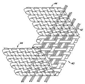
Figure 6 illustrates a three-dimensional packaging
structure; and
Figure 7 illustrates another application of the
invention in which the optical fibers extend beyond the
material to permit easier interconnection.
DESCRIPTION OF THE SPECIFIC EMBODIMENT
Figure 1 is a plan view of a preferred embodiment
of material fabricated according to the invention. As
illustrated, the material is woven with warp strands 10A,
108, 10C, 10D, and woof (or pick) strands 11A, 118, 11C and
11D. The warp and woof strands are woven together into a
fabric-like material using a normal over-and-under plain
weave pattern. The warp and woof strands may employ any
desired material having the physical properties desired for
the application. Far example, the strands can comprise
fiberglass, gy~aphite, silica carbide, or other materials<
An example of a silica carbide fiber suitable for
application is sold by Dow-Corning Corporation under the
trademark Nicalon"'.
Introduced with the supporting fibers before the
weaving are optical fibers 12A, 12B, 12C, 12D, 12E and 12F.
Importantly, the optical fibers are introduced into the
material to run in the warp direction with a zero warp.
That is, the optical fibers have no bending or crimping.
The absence of bends or crimps provides maximum optical
efficiency and provides repeatability of signals regardless
of their transmission position within the woven material.
It is well known that when signals are tr2~nsmitted through
optical fibers, losses occur wherever bending or kinking of
the fiber is present. The structure shown in Figure 1
includes a pair of optical fibers in the channel between
each non-optical warp strand 10A, ...10D. Of course, more
or fewer optical fibers may be employed~
CA 02063372 2001-O1-29
78626-2
6
Figure 2 is a cross-sectional. view of material such
as depicted in Figure 1, but which has also been coated with a
protective coating material to hold all fibers in place.
Figure 2 can be considered to be a cross-sectional view of the
structure shown in Figure 1 taken along the length of fiber
12A. As shown in Figure 2, the optical fiber 12A extends
across the figure with woof strands 11A, 11B, 11C and 11D
extending over and under the optical fiber. A coating 20
consisting of a well known material such as rubber, epoxy, or
other suitable material, holds the optical fibers in position
with respect to the surrounding material.
Figure 3 depicts a larger region of material woven
according to the preferred embodiment to illustrate the manner
in which the woof strands are bound at the edges of the
material. As shown in Figure 3, the optical fibers 12 extend
from the top of the figure to the bottom, while the woof
strands extend across the figure from left to right. Also
extending from the top of the figure to the bottom are the warp
strands discussed above in conjunction with Figure 1. The
edges of the woof strands shown as 1A, 1B, 1C, and 1D are bound
by a conventional technique using leno material 31 and 32. Of
course, other techniques may also be employed to secure the
edges of the fabric, for example by knotting them together.
For the embodiment depicted in Figure 3, silica
carbide fibers such as those described above are employed which
have a dimension of 1800 denier and are woven with a density of
44 optical fibers per inch. The density of the weave is
defined both by the diameter of the optical fiber, the
surrounding material and the width of the teeth of the comb,
and is variable as necessary depending upon the application.
The optical fibers embodied in the fabric depicted in
CA 02063372 2001-O1-29
78626-2
6a
Figure 3 are commercially-available optical fibers such as
graded index GE-doped silica fibers manufactured by Corning or
single mode silica fibers, etc. In one embodiment Corning
fibers with an numerical aperture of 0.22, a core of 125
microns with an overall diameter of 250 microns and an 85°C
temperature rating are employed.
7
Using fibers such as these in a material as described
results in about 44 fibers per lineal inch across the
material. The length of the material is dependent on the
length of the roll of material used, and very long calls of
material, exceeding a kilometer in length, can be fabricated
using existing commercially-available weaving equipment with
adequate tension control methods applied. The optical
fibers can be positioned, and the surrounding material
woven, using conventional textile weaving equipment. For
example, a composite generation facility with standard
weaving equipment can be employed. Preferably, a comb will
be employed in addition to the standard weaving equipment to
position the optical fibers. The comb can be in the form of
a small-toothed comb installed at the front end of the
weaving equipment. Such a comb provides a reproducible
number of fiber optic strands between the strands of the
intervening material and assures a nonoverlapping condition
with unbent optical fiber. Although various commercial
machines will require different adjustments, during ane test
2o of the weaving operation, a change in tension occurred when
the weaving spinner callers ran out of fiber. This change
in tension can cause breakage of the optical fiber, and
accordingly the importance of controlling proper tension by
suitable monitoring and maintenance of full rollers is
believed to be important. In the prior art and presently,
optical fibers were laid out manually in composite plies in
specific orientation. Misalignment of the optical fiber
orientation xesults in significant losses. Tn the
techniques described herein, the laying out of the fiber is
achieved automatically in the normal weaving grocess.
Reducing such losses provides for a uniformity and
repeatability that lends itself to accurate and diverse
mada~.sty sensing and simple interconnect processes. One of
the most important issues is sensor network integration
within the structure. This invention successfully addresses
this issue as it relates to major systems.
For the embodiment depicted in Figure 3, two
optical fiber yarns are placed in the.channel between each
CA 02063372 2001-O1-29
78626-2
8
of the warp strands. It. should be understood, however, that
any desired number of optical fibers can be placed between each
of the warp strands. For example, in one embodiment each
channel contains eight optical fibers. Other embodiments are
discussed below.
Once the material has been woven with the optical
fibers in position, the assembly may be coated with a desired
material to give added protection to the structure. As
described in conjunction with Figure 2, by applying a coating
to the woven grid-like mat, the position of the fibers in the
plane of the grid-like mat is fixed, and the material is
provided with additiona7_ rigidity. Preferably, the curing
material can be applied by brushing it onto the woven sheet, by
passing the woven sheet through a bath of curing material, or
by employing other conventional application techniques.
In one embodiment of the invention, the rigid coating
was made using a curing fluid made from the EPON 828* epoxy,
manufactured by Shell Chemical Company, mixed with a fixing
agent of diethylene-triamine in a ratio of 88% epoxy and 12%
fixing agent by volume. In other embodiments where a flexible
material is desired, commercial grade rubber cement has been
employed.
Figure 4 illu~;trates another embodiment of the
invention as ribbons of material. As shown there, the material
is divided into two sections, 51, and 53. These sections are
separated by additional longitudinal leno filaments 54 and 55,
and an extra support fiber 57. Numeral 56 indicates a position
for separation of a portion of the matrix from another portion
as does numeral 57. The leno filaments 54 and 55 provide a
convenient place where the optic grid can be separated into
* Trade-mark
CA 02063372 2001-O1-29
78626-2
8a
individual ribbons, provide a convenient marker for identifying
particular fibers, as well as preventing the material from
unraveling. Of course, any desired number of sections can be
used in the material. In this manner, a large loom can be used
to weave in parallel wid.t.hs of like or varied materials later
divided into sections f.or various uses.
Figure 5 dep~.cts another embodiment of the invention
in which eight optical fibers 61, 62, ...68 are
9
positioned in pairs between two support fibers. Lenos 64
with associated extra support fibers 75 and 76 are provided
to enable one strip of material to be fabricated with a
number of sections and then divided into separate pieces if
desired.
Figure 6 illustrates a three-dimensional woven
structure suitable for various packaging considerations. As
shown, the structure includes a woven backplane 40 with
fiber optic conductors 42 and two woven planes 44
approximately perpendicular to the backplane. This
structure can be used to support printed circuit boards
and/or wafers which interface to the fiber option in the
backplane. This section could be at various angles relative
to the backplane. It is suggested that sharp angles be
avoided. All sections moving out of the plane should be
rounded at an angle no less than the specified radius in the
optical fiber data sheets. This avoids undue stress at
sharp edges of the supporting material. Coatings applied to
the material can supply additional stress relief.
Figure 7 is a perspective view illustrating how
the material shown in Figures 1, 2 and 3 may be fabricated
into a three-dimensional structure. For the structure
depicted in Figure 7, the optical fibers 12 extend beyond
one edge of the woven material to facilitate optical
connections. As also shown in Figure 7, the warp fibers 10
are woven through the material in a continuous fashion. By
extending the material beyond the area where the optical
fibers are woven into the mat, an additional area of
supporting material provides a structure for mounting other
components 15. Of course, components 15 may also be mounted
proximate to the optical fibers to enable connections at
that location as well. Components 15 will typically
comprise electronic, optical or electrooptical components.
As one example, an optical detector integrated circuit can
~5 be mounted on the woven cloth mat, and appropriate
connections made to surrounding integrated circuits using
wire bonding, flexible printed circuit connections, or other
10
well known techniques. of course, circuits can be mounted
on either or both sides of the material.
Before or after mounting the circuits, depending
upon the particular application, the structure shown in
Figure 7 can be coated with an appropriate material to hold
it in a rigid position or to allow it to flex.
As shown in Figure 7, the material of this
invention provides a structure which facilitates various
packaging techniques for circuits. i~lith the structure
depicted, the optical fibers are held in a precise location
facilitating connection to other integrated circuits or
other optical elements. Similarly, by extending the woven
material beyond the circuit substrate portion, a convenient,
inexpensive, integrated technique for mounting circuit
elements for ca~nneation to the optical fibers is provided.
Of course, sensors may be connected to individual fibers or
groups of fibers to provide large arrays of sensors. In
addition, the optical fibers themselves can be used as
sensing elements to provide a smart skin array. Examples of
such applications of '°smart" skin arrays are described in
the two technical papers referred to above. The '°smart"
skin can provide fiber optic sensing arrays in the skin of
airplanes. It can be used to fabricate low cost, high speed
communications for computer networks. For example, the
material can be employed as an optoelectronic backplane for
large scale, high performance computer systems, such as
parallel processors.
The material of the invention also provides a
structure for transmission and reception of laser-generated
optical signals in conjunction with packaging and
interconnecting components. Such embodiments can be used to
provide high speed data buses to interconnect components in
a high performance computer system. Of course, the use of
large numbers of optical fibers provides an ease in
constructing systems wherein redundant means for
transmission of information is desired as well as for
multichannel information transfers.
~0633~2
11
Although the foregoing invention has bean shown
and described with respect to preferred embodiments, it will
be understood that many alternative embodiments can employ
the techniques described here. Accordingly, the scope of
the invention is set forth by the following claims.