Note: Descriptions are shown in the official language in which they were submitted.
WO 90/1~4~4 ~ `. c~ .; .t PCr/US90/02678
VOLTAGE CONTROL OSCILLATOR WITH
AUTOMATIC CURRENT CONTROL
Technical Field
This invention relates generally to control circuitry for
controlling the oscillator current in a voltage-controlled oscillator
1 5 (VGO).
Backaround Art
Known circuits for controlling VCOs use feedback circuits
th~t sense the power output of the VCO and rectify that power for
controlling the gain of the VCO. However, sensing radio-
frequency power is inadequate if one seeks to maintain noise at a
minimum.
Summar~of the InventîQn
Accordingly, it is an object of the present invention to
provide a control circuit that senses a direct current (DC) signal
that is indicative of the oscillation current or that senses an
alternating current (AC) signal indicative of the VCO bias state
and filters out the AC before the feedback signal is produced. It is
another object of the invention to provide an oscillator current
control circuit that maintains a minimum noise level throughout a
broad spectrum of frequencies while maintaining the power
output substantially constant.
Briefly, according to the invention, the oscillator bias
voltage of a VCO is controlled in such a manner as to maintain a
- constant oscillation current output. A comparator is used tocompare a DC voltage, sensed at a point in the VCO wherein the
, ~
:,
WO 90/15484 PCT/US91)/1)267
current of the VCO may be determined, with a reference voltage
that is indicative of the desired level of th0 oscillator current. The
output of the comparator is applied back to the VCO so that the
oscillator bias voltage is changed to maintain the oscillation
5 current costant.
The voltage sensed in the VCO may be AC as long as a
low pass filter is provided between the sensing point and the
comparator to filter out the AC component of the sensed voltage.
10 Brief Description of the Drawina~
Figure 1 is a block diagram of an automatic current control
circuit in accordance with the invention.
Figure 2 is a schematic of an embodiment of the automatic
current control circuit with an emitter sensing point tor the
15 ~eedback loop including a current cut-back circuit.
Figure 3 is a schematic of another embodiment of the
automatic current control circuit with an emitter DC sensing point
for the feedback loop wherein no low pass filter is needed.
Figure 4 is a schematic of another embodiment of the
20 automatic current control circuit with a collector sensing point for
the feedback loop.
- Detailed Descril~tion of the Preferred Embodiment
Referring to Figure 1, a block diagram of an automatic
25 current control circuit 100 in accordance with the invention is
shown. A voltage is sensed, in a voltage-controlled oscillator
(VCO), that represents the oscillation current state of the
oscillator. That voltage is then applied to a low-pass filter 104, by
a line 103, for filtering out of the alternating-current (AC)
30 component of the sensed voltage. The output (V2) of the low-
pass filter is applied to a first input 105 of a comparator 106 for
comparing with a reference voltage (V1). The output (V3) of the
comparator 106 is applied back to the VCO by a line 107 to
control the oscillator bias voltage.
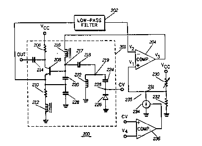
Referring to Figure 2, an embodiment of the automatic
current control circuit 200 is shown. A VCO 201 comprises a
bipolar oscillator transistor 208 with its base coupled to a node
WO 90/154~4 ". ;~ PCl/~ ()/U~7
217, its collector coupled to the supply voltage (Vcc) (through a
resistor 206) and its emitter coupled to ~round, through a resistor
210 and through a high frequency choke 212. The emitter is also
coupled to a terminal of capacitors 220 and a terminal of
capacitor 228 at a node ~09.
A choke 216 has a terminal coupled with a terminal of ~
capacitor 220 and a terminal of a capacitor 218 at node 217. The
other terminal of capacitor 228 is coupled to ground and the other
terminal of capacitor 218 is coupled to a node 219. An inductor
1 0 222 is disposed between ground and the node 219. A capacitor
224 is disposed between the node 219 and a node 225. A
varactor diode 226 has its cathode coupled to the node 225 and
its anode coupled to ground. A control voltage (CV) is applied at
node 225 to control the frequency of the VCO 201.
1 5 A voltage that represents the current state of the VCO 201,is sensed at the emitter 209 of transistor 208 and applied to a low-
pass ~ilter 202. The output (V2) of the low-pass filter 202 is
applied to a first (negative) input of a comparator 204 for
comparison with a reference voltage (V1) present at the posi~ive
20 input of the comparator 204. The output (V3) of the comparator
204 is applied to the base of the oscillation transistor 208, through
the choke 216, thus changing the voltage at node 217,
as a function of the difference between voltages V1 and V2.
Thus, the oscillator current is kept constant by compa~ing voltage
25 V1 (which is adjusted by the user) with voltage V2 (the DC
voltage developed by current flowing in the oscillator) and
automatically adjusting the voltage V3 (which is also the base
bias voltage of the VCO 201).
A current cut-back circuit 235 comprises a comparator 236
30 with inputs V4 and CV (the control voltage) and a current source
234 that is controlled by the output of the comparator 236 . The
current source 234 is disposed between node 231 and ground.
The current cut-back circuit 235 operates only when the varactor
control voltage, CV, is greater than voltage V4. When CV is less
35 than V4 the current flowing through current-source 234 is zero
and thus V1 is not aitered. When CV is greater than V4, the
current begins to flow through current-source 234, lowering the
WO 90/1~484 PCr/US~O/l~267
k 4
voltage V1 at node 231 and consequently !owering V3. A lower
V3, in turn, results in a lower oscillator current.
The reference voltage V1 is selected in an adjustable
circuit comprising an adjustable resistor, or potentiometer 230,
5 disposed between the voltage supply (Vcc) and a node 231, and
a resistor 232 disposed between the node 231 and ground. ~
As the reverse bias on the varactor diode 226 increases,
the VCO frequency increases and the quality factor of the varactor
diode 226 also increases. Thus the VCO requires less current tor
10 optimum phase noise performance and power output . Thus, the
addition of the current cut-back circuit 235 decreases the VCO
current as CV rises.
Referring to Figure 3, another embodiment 300 of the
invention is shown wherein the feedback voltage of the VCO 306
15 is sensed at a DC point in the VCO 306. The circuit configuration
of VCO circuit 300 differs from that of the VCO circuit 200
described in reference to Figure 2 only in three respects: (1 ) VCO
circuit 300 does not include the current cut-back circuit 235 of
VCO circuit 200; (2) VCO circuit 300 does not include the low-
20 pass filter 202 of VCO circuit 200; and (3) the feedback volage of
VCO circuit 300 is sensed at a DC node 321 because of the
position of choke 320 which filters out the AC current flowing from
the collector of transistor 308 to its emitter. The necessity for a
low-pass filter is also eliminated by sensing the feedback voltage
25 at DC point 321. In all other respects the VCO circuit 300
operates in the same way as VCO circuit 200.
Referring to Figure 4, a further enbodiment of the invention
is shown. A VCO circuit 400 includes a feedback loop that
senses an AC voltage at a node 404 at the collector of transistor
30 402. The VCO circuit 400 operates in substantially the way as the
VCO circuit 200 described with respect to Figure 2, and its
operation only differs in that there is no current cut-back circuit
included in VCO circuit 400 and that the sensing point for the
feedback voltage is at the collector of the oscillation transistor 402
35 instead of at its emitter.
, ~
i ~ What is claimed is: