Sélection de la langue

Search

Sommaire du brevet 2063404 

Énoncé de désistement de responsabilité concernant l'information provenant de tiers

Une partie des informations de ce site Web a été fournie par des sources externes. Le gouvernement du Canada n'assume aucune responsabilité concernant la précision, l'actualité ou la fiabilité des informations fournies par les sources externes. Les utilisateurs qui désirent employer cette information devraient consulter directement la source des informations. Le contenu fourni par les sources externes n'est pas assujetti aux exigences sur les langues officielles, la protection des renseignements personnels et l'accessibilité.

Disponibilité de l'Abrégé et des Revendications

L'apparition de différences dans le texte et l'image des Revendications et de l'Abrégé dépend du moment auquel le document est publié. Les textes des Revendications et de l'Abrégé sont affichés :

  • lorsque la demande peut être examinée par le public;
  • lorsque le brevet est émis (délivrance).
(12) Brevet: (11) CA 2063404
(54) Titre français: OSCILLATEUR A COMMANDE AUTOMATIQUE PAR TENSION
(54) Titre anglais: VOLTAGE CONTROL OSCILLATOR WITH AUTOMATIC CURRENT CONTROL
Statut: Périmé et au-delà du délai pour l’annulation
Données bibliographiques
(51) Classification internationale des brevets (CIB):
  • H03L 07/00 (2006.01)
  • H03B 05/12 (2006.01)
  • H03L 01/00 (2006.01)
  • H03L 05/00 (2006.01)
(72) Inventeurs :
  • KEHLER, WALTER H., JR. (Etats-Unis d'Amérique)
(73) Titulaires :
  • MOTOROLA, INC.
(71) Demandeurs :
  • MOTOROLA, INC. (Etats-Unis d'Amérique)
(74) Agent: GOWLING WLG (CANADA) LLP
(74) Co-agent:
(45) Délivré: 1993-09-21
(86) Date de dépôt PCT: 1990-05-17
(87) Mise à la disponibilité du public: 1990-12-03
Requête d'examen: 1991-10-29
Licence disponible: S.O.
Cédé au domaine public: S.O.
(25) Langue des documents déposés: Anglais

Traité de coopération en matière de brevets (PCT): Oui
(86) Numéro de la demande PCT: PCT/US1990/002678
(87) Numéro de publication internationale PCT: US1990002678
(85) Entrée nationale: 1991-10-29

(30) Données de priorité de la demande:
Numéro de la demande Pays / territoire Date
360,627 (Etats-Unis d'Amérique) 1989-06-02

Abrégés

Abrégé anglais

2063404 9015484 PCTABS00002
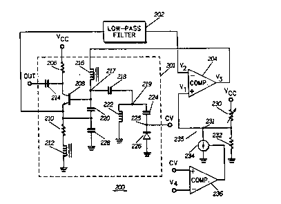
An automatic voltage-controlled oscillator (VCO) current control
circuit (100, 200, 300 or 400) that senses a voltage in the VCO
(201) representative of the current of the VCO (201), compares
that voltage (V2) to a reference voltage (V1), and applies the
voltage (V3) resulting from that comparison back to the VCO (201) at a
point therein that changes its bias state in such a manner as to
maintain the noise level in the VCO at a minimum and also
maintains the power output of the oscillator substantially constant.

Revendications

Note : Les revendications sont présentées dans la langue officielle dans laquelle elles ont été soumises.


WO 90/15484 PCT/US90/02678
Claims
1. A circuit for controlling oscillation current in an
oscillator comprising:
a comparator for comparing a level of sensed
voltage, that is representative of the oscillation current state of
said oscillator, with a first reference voltage;
means for providing said first reference voltage for
comparison with said sensed voltage;
said comparator providing an output that is coupled
to said oscillator so that the oscillator current is maintained at an
optimum level for minimizing the phase noise and substantially
levelling the power of said oscillator.

2. The circuit of claim 1, wherein said sensed voltage is direct-current (DC)
voltage.
3. The circuit of claim 1, further comprising a low-pass filter disposed between
said oscillator and said comparator for filtering out alternating-current (AC) components
of said sensed voltage.
4. The circuit of claim 1, wherein said oscillator comprises a bipolar oscillation
transistor.
5. The circuit of claim 1, further comprising a means for reducing said first
reference voltage when a control voltage, that is used to control the frequency at which said
oscillator oscillates, is greater than a second reference voltage selected to compensate for
any changes in the equivalent positive resistance of said oscillator as a result of maintaining
the noise level of said oscillator at a minimum.
6. The circuit of claim 6, wherein the means for reducing said first reference
voltage comprises a comparator for comparing said second reference voltage to said control
voltage, said comparator being coupled to said means for providing said first reference
voltage.
7. The circuit of claim 4, wherein said sensed voltage is sensed at a node coupled
to the emitter of said oscillation transistor.
8. The circuit of claim 4, wherein said sensed voltage is sensed at a node coupled
to the collector of said oscillation transistor.
9. The circuit of claim 4, further comprising a radio-frequency choke having first
and second terminals, said first terminal being coupled to the emitter of said oscillation
transistor and wherein said sensed voltage is sensed at a node coupled to said second
terminal.

WO 90/15484 PCT/US90/02678
10. The circuit of claim 4, further comprising a radio-
frequency choke having first and second terminals, said first
terminal being coupled to the emitter of said oscillation transistor
and wherein said sensed voltage is sensed at a node coupled to
said second terminal.

WO 90/15484 PCT/US90/02678
11. A method for controlling the oscillation current of an
oscillator comprising:
sensing a level of sensed voltage in said oscillator,
said sensed voltage representing the oscillation current state of
said oscillator;
comparing said level of sensed voltage with a level
of reference voltage to obtain a differential voltage that is
proportional to the difference between said level of sensed
voltage and said level of reference voltage; and
applying said differential voltage to a point in said
oscillator that controls its bias so that the noise level in said
oscillator is maintained at a minimum level and the power output
of said oscillator is maintained at a substantially constant level.

Description

Note : Les descriptions sont présentées dans la langue officielle dans laquelle elles ont été soumises.


WO 90/1~4~4 ~ `. c~ .; .t PCr/US90/02678
VOLTAGE CONTROL OSCILLATOR WITH
AUTOMATIC CURRENT CONTROL
Technical Field
This invention relates generally to control circuitry for
controlling the oscillator current in a voltage-controlled oscillator
1 5 (VGO).
Backaround Art
Known circuits for controlling VCOs use feedback circuits
th~t sense the power output of the VCO and rectify that power for
controlling the gain of the VCO. However, sensing radio-
frequency power is inadequate if one seeks to maintain noise at a
minimum.
Summar~of the InventîQn
Accordingly, it is an object of the present invention to
provide a control circuit that senses a direct current (DC) signal
that is indicative of the oscillation current or that senses an
alternating current (AC) signal indicative of the VCO bias state
and filters out the AC before the feedback signal is produced. It is
another object of the invention to provide an oscillator current
control circuit that maintains a minimum noise level throughout a
broad spectrum of frequencies while maintaining the power
output substantially constant.
Briefly, according to the invention, the oscillator bias
voltage of a VCO is controlled in such a manner as to maintain a
- constant oscillation current output. A comparator is used tocompare a DC voltage, sensed at a point in the VCO wherein the
, ~
:,

WO 90/15484 PCT/US91)/1)267
current of the VCO may be determined, with a reference voltage
that is indicative of the desired level of th0 oscillator current. The
output of the comparator is applied back to the VCO so that the
oscillator bias voltage is changed to maintain the oscillation
5 current costant.
The voltage sensed in the VCO may be AC as long as a
low pass filter is provided between the sensing point and the
comparator to filter out the AC component of the sensed voltage.
10 Brief Description of the Drawina~
Figure 1 is a block diagram of an automatic current control
circuit in accordance with the invention.
Figure 2 is a schematic of an embodiment of the automatic
current control circuit with an emitter sensing point tor the
15 ~eedback loop including a current cut-back circuit.
Figure 3 is a schematic of another embodiment of the
automatic current control circuit with an emitter DC sensing point
for the feedback loop wherein no low pass filter is needed.
Figure 4 is a schematic of another embodiment of the
20 automatic current control circuit with a collector sensing point for
the feedback loop.
- Detailed Descril~tion of the Preferred Embodiment
Referring to Figure 1, a block diagram of an automatic
25 current control circuit 100 in accordance with the invention is
shown. A voltage is sensed, in a voltage-controlled oscillator
(VCO), that represents the oscillation current state of the
oscillator. That voltage is then applied to a low-pass filter 104, by
a line 103, for filtering out of the alternating-current (AC)
30 component of the sensed voltage. The output (V2) of the low-
pass filter is applied to a first input 105 of a comparator 106 for
comparing with a reference voltage (V1). The output (V3) of the
comparator 106 is applied back to the VCO by a line 107 to
control the oscillator bias voltage.
Referring to Figure 2, an embodiment of the automatic
current control circuit 200 is shown. A VCO 201 comprises a
bipolar oscillator transistor 208 with its base coupled to a node

WO 90/154~4 ". ;~ PCl/~ ()/U~7
217, its collector coupled to the supply voltage (Vcc) (through a
resistor 206) and its emitter coupled to ~round, through a resistor
210 and through a high frequency choke 212. The emitter is also
coupled to a terminal of capacitors 220 and a terminal of
capacitor 228 at a node ~09.
A choke 216 has a terminal coupled with a terminal of ~
capacitor 220 and a terminal of a capacitor 218 at node 217. The
other terminal of capacitor 228 is coupled to ground and the other
terminal of capacitor 218 is coupled to a node 219. An inductor
1 0 222 is disposed between ground and the node 219. A capacitor
224 is disposed between the node 219 and a node 225. A
varactor diode 226 has its cathode coupled to the node 225 and
its anode coupled to ground. A control voltage (CV) is applied at
node 225 to control the frequency of the VCO 201.
1 5 A voltage that represents the current state of the VCO 201,is sensed at the emitter 209 of transistor 208 and applied to a low-
pass ~ilter 202. The output (V2) of the low-pass filter 202 is
applied to a first (negative) input of a comparator 204 for
comparison with a reference voltage (V1) present at the posi~ive
20 input of the comparator 204. The output (V3) of the comparator
204 is applied to the base of the oscillation transistor 208, through
the choke 216, thus changing the voltage at node 217,
as a function of the difference between voltages V1 and V2.
Thus, the oscillator current is kept constant by compa~ing voltage
25 V1 (which is adjusted by the user) with voltage V2 (the DC
voltage developed by current flowing in the oscillator) and
automatically adjusting the voltage V3 (which is also the base
bias voltage of the VCO 201).
A current cut-back circuit 235 comprises a comparator 236
30 with inputs V4 and CV (the control voltage) and a current source
234 that is controlled by the output of the comparator 236 . The
current source 234 is disposed between node 231 and ground.
The current cut-back circuit 235 operates only when the varactor
control voltage, CV, is greater than voltage V4. When CV is less
35 than V4 the current flowing through current-source 234 is zero
and thus V1 is not aitered. When CV is greater than V4, the
current begins to flow through current-source 234, lowering the

WO 90/1~484 PCr/US~O/l~267
k 4
voltage V1 at node 231 and consequently !owering V3. A lower
V3, in turn, results in a lower oscillator current.
The reference voltage V1 is selected in an adjustable
circuit comprising an adjustable resistor, or potentiometer 230,
5 disposed between the voltage supply (Vcc) and a node 231, and
a resistor 232 disposed between the node 231 and ground. ~
As the reverse bias on the varactor diode 226 increases,
the VCO frequency increases and the quality factor of the varactor
diode 226 also increases. Thus the VCO requires less current tor
10 optimum phase noise performance and power output . Thus, the
addition of the current cut-back circuit 235 decreases the VCO
current as CV rises.
Referring to Figure 3, another embodiment 300 of the
invention is shown wherein the feedback voltage of the VCO 306
15 is sensed at a DC point in the VCO 306. The circuit configuration
of VCO circuit 300 differs from that of the VCO circuit 200
described in reference to Figure 2 only in three respects: (1 ) VCO
circuit 300 does not include the current cut-back circuit 235 of
VCO circuit 200; (2) VCO circuit 300 does not include the low-
20 pass filter 202 of VCO circuit 200; and (3) the feedback volage of
VCO circuit 300 is sensed at a DC node 321 because of the
position of choke 320 which filters out the AC current flowing from
the collector of transistor 308 to its emitter. The necessity for a
low-pass filter is also eliminated by sensing the feedback voltage
25 at DC point 321. In all other respects the VCO circuit 300
operates in the same way as VCO circuit 200.
Referring to Figure 4, a further enbodiment of the invention
is shown. A VCO circuit 400 includes a feedback loop that
senses an AC voltage at a node 404 at the collector of transistor
30 402. The VCO circuit 400 operates in substantially the way as the
VCO circuit 200 described with respect to Figure 2, and its
operation only differs in that there is no current cut-back circuit
included in VCO circuit 400 and that the sensing point for the
feedback voltage is at the collector of the oscillation transistor 402
35 instead of at its emitter.
, ~
i ~ What is claimed is:

Dessin représentatif
Une figure unique qui représente un dessin illustrant l'invention.
États administratifs

2024-08-01 : Dans le cadre de la transition vers les Brevets de nouvelle génération (BNG), la base de données sur les brevets canadiens (BDBC) contient désormais un Historique d'événement plus détaillé, qui reproduit le Journal des événements de notre nouvelle solution interne.

Veuillez noter que les événements débutant par « Inactive : » se réfèrent à des événements qui ne sont plus utilisés dans notre nouvelle solution interne.

Pour une meilleure compréhension de l'état de la demande ou brevet qui figure sur cette page, la rubrique Mise en garde , et les descriptions de Brevet , Historique d'événement , Taxes périodiques et Historique des paiements devraient être consultées.

Historique d'événement

Description Date
Inactive : CIB de MCD 2006-03-11
Le délai pour l'annulation est expiré 2002-05-17
Lettre envoyée 2001-05-17
Accordé par délivrance 1993-09-21
Exigences pour une requête d'examen - jugée conforme 1991-10-29
Toutes les exigences pour l'examen - jugée conforme 1991-10-29
Demande publiée (accessible au public) 1990-12-03

Historique d'abandonnement

Il n'y a pas d'historique d'abandonnement

Historique des taxes

Type de taxes Anniversaire Échéance Date payée
TM (brevet, 8e anniv.) - générale 1998-05-19 1998-04-06
TM (brevet, 9e anniv.) - générale 1999-05-17 1999-04-06
TM (brevet, 10e anniv.) - générale 2000-05-17 2000-04-04
Titulaires au dossier

Les titulaires actuels et antérieures au dossier sont affichés en ordre alphabétique.

Titulaires actuels au dossier
MOTOROLA, INC.
Titulaires antérieures au dossier
WALTER H., JR. KEHLER
Les propriétaires antérieurs qui ne figurent pas dans la liste des « Propriétaires au dossier » apparaîtront dans d'autres documents au dossier.
Documents

Pour visionner les fichiers sélectionnés, entrer le code reCAPTCHA :


Pour visualiser une image, cliquer sur un lien dans la colonne description du document. Pour télécharger l'image (les images), cliquer l'une ou plusieurs cases à cocher dans la première colonne et ensuite cliquer sur le bouton "Télécharger sélection en format PDF (archive Zip)" ou le bouton "Télécharger sélection (en un fichier PDF fusionné)".

Liste des documents de brevet publiés et non publiés sur la BDBC .

Si vous avez des difficultés à accéder au contenu, veuillez communiquer avec le Centre de services à la clientèle au 1-866-997-1936, ou envoyer un courriel au Centre de service à la clientèle de l'OPIC.


Description du
Document 
Date
(aaaa-mm-jj) 
Nombre de pages   Taille de l'image (Ko) 
Dessins 1997-10-27 2 58
Abrégé 1997-10-27 1 53
Revendications 1997-10-27 4 98
Description 1997-10-27 4 224
Dessin représentatif 1999-02-09 1 10
Avis concernant la taxe de maintien 2001-06-13 1 178
Taxes 1997-04-13 1 71
Taxes 1996-04-14 1 60
Taxes 1994-03-21 1 70
Taxes 1993-03-22 1 95
Taxes 1992-03-12 1 34
Taxes 1995-04-17 1 61
Rapport d'examen préliminaire international 1991-10-28 10 273
Correspondance de la poursuite 1991-10-28 2 26
Correspondance reliée au PCT 1993-06-27 1 28
Courtoisie - Lettre du bureau 1992-10-15 1 41