Note: Descriptions are shown in the official language in which they were submitted.
~~~C~~~~
FIELD OF THE INVENTION
The present invention relates generally to the
monitoring of defective conditions within batteries and more
particularly, to 'the detection of such conditions from battery
cell voltage output.
EACKGgtOUND OF THE INVENTION
Apparatus for detecting most battery defects is well
known. However, 'this apparatus usually monitors a parameter,
such as abnozfinal voltage or current or power output relative to
ZO the overall battery, rather than to the individual cells thereof.
For some types of defects, this averall battery approach is clear-
ly inadequate. One such defect is found in a lithium type bat-
tery which often presents a dangerous pressure buildup therein
when one or more of its cells has an abnormally low voltage out-
put. The conventional approach for monitoring this defect is 'to
mechanically sense the pressure within the overall battery and
then appropriate corrective action is initiated at some critical
pressure level. Because the operating tolerances of the mechan-
ical pressure sensor are very wide, the critical pressure level
20 of this approach must be significantly lower than desired to
attain the required safety factor.
SUMMARY OF THE INZTENTION
It is the general object of the present invention to mon-
itor the voltage output from the individual cells of a battery
with those cells referenced to a common ground.
_1_
It is a specific object of the present invention to
accomplish the above~stated general object in a detector for
indicating when pressure within at least one cell of a lithium
type battery reaches a dangerous level.
These and other objects are accomplished in accordance
with the present invention by referencing all of the battery
cells to a common ground and generating a control signal when the
voltage output from at least one of the cells is abnormal. The
conductivity of at least one electrical path is changed in re-
sponse to that signal when the invention is incorporated into a
battery defect detector. In one embodiment, the signal is gener-
ated relative to each cell by a threshold detector when a differ-
ential amplifier senses that a predetermined voltage output has
been reached for that cell. Operational amplifiers are individu-
ally arranged.as the differential amplifier and the threshold de-
tector for each cell in this embodiment. At least one electronic
switch is utilized in the battery detector embodiment of the
invention and responds to the control signal by changing its
conductivity. Various arrangements of bipolar and/or field
effect transistors can be utilized for such electronic switch-
ing. Capacitors may also be incorporated in such embodiments to
attain switching stability.
The scope of the present invention is only limited by
the appended claims for which support is predicated,on the pre-
ferred embodiments hereinafter set forth in the following descrip-
tion and the attached drawings wherein like reference characters
relate. to like parts throughout the several figures.
_z_
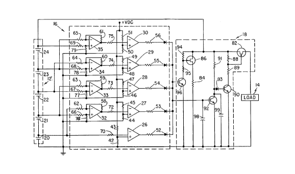
DESCRTPTTON OF THE DRA'WTNGS
FTG. 1 is a block diagram of battery powered apparatus
having the invention incorporated thereinr and
FTG. 2 is a schematic/block diagram of the invention
incorporated in apparatus which remedies the danger presented
when a pressure buildup occurs wirthin at least one cell of a
lithium type battery.
DESCRTPTTON OF THE PREFERRED EMBODIMENTS
The invention described herein relates broadly to appara-
tus for monitoring a defective condition within a battery having
a plurality of cells. As shown in FIG. 1, such apparatus can be
implemented within any circuit 10 wherein a battery 12 is incor-
porated to supply current to a load 14. Ey way of the invention,
a means Z6 is incorporated for referencing the cells of the bat-
tery 12 to a common ground while generating a control signal when
the voltage output from at least one battery cell becomes abnor-
mal to indicate the defective condition. Of course, the control
signal may be generated either for abnormally high voltage output
or for abnormally low voltage output within 'the broad scope of
the invention. Also, a switch means 1~ for responding to the
control signal by changing the conductive state of at least one
electrical path thraugh which current flows from the battery 12,
may be u-~ilized for indicating when a defective condition occurs
andlor for remedying a danger presented by that condition.
_3_
Although the invention has many applications in which
different embodiments thereof would be utilized, FTG. 2 relates
to a particular application thereof for which dangerous pressure
buildups within a lithium type battery 12' having a plurality of
cells 20, 21, 22, 23, 24 must be detected and remedied. As is
well known in the electrochemical arts, lithium type batteries
characteristically develop large quantities of gas when the volt-
age output from one or more of ths:ir cells is abnormally low. Of
course, this gas accumulates internally within such batteries and
ZO causes a pressure buildup which presents a dangerous situation
due to the possibility of explosion. One approach for remedying
this dangerous situation is to disconnect the load 14 from the .
battery 12' as quickly as possible, and dissipate the charge in
the battery 12' at a safe rate.
In the FIG. 2 embodiment, the signal generating means 16
includes threshold detectors 26, 27, 28, 29 and 30 which individu-
ally derive the control signal when the voltage output from one
of the cells 20-24 respectively, reaches a predetexznined
reference level and differential amplifiers 32, 33, 34 and 35
20 which individually detect the voltage output from one of the
cells 21-24 respectively, that have no direct connection to
ground. Each of the threshold detectors 27-30 functions in
cooperation with one of the individual different3.a.1 amplifiers
32-35 respectively, and except for the added cost and power
consumption thereof, a differential amplifier (not~shown) could
be including for threshold detector 26 withiw the scope of this
invention. Because the battery must be both disconnected and
-4-
~~P~~~
discharged to accomplish the above mentioned approach for
remedying 'the dangerous battery si'tua'tion, the switch means ~,$ in
the FzG. 2 embodiment must control the conductivity through at
least two electrical paths. However, only the conductivity
through one electrical path need be controlled in other
applications for which the invention could be utilized.
Conventionally arranged operational amplifiers serve as
both the threshold detectors 26-31~ and the differential ampli-
fiers 32-35 in the signal generating means 16 of FIG. 2. As is
well known to those skilled in the electronic arts, each opera-
tional amplifier includes an output connection, along with in-
verting and non-inverting signal input connections. Also each
operational amplifier is energized with a DC bias voltage applied
across positive and negative power input connections (not shown).
Each threshold detector 26-30 includes an input terminal at the
inverting input connection of its operational amplifier, a
threshold set terminal at the non-inverting input connection of
its operational amplifier, and an output terminal at the output
connection of its operational amplifier. Functionally, each
threshold detectrar 26-30 produces a low level signal at its out-
put terminal when the voltage level at its input terminal exceeds
the voltage level at its threshold set terminal and otherwise, a
high level signal is produced thereat. A predetermined voltage
level relative to ground is applied to the threshold set terminal
of each thresho~.d detector 26-30 in accordance with the battery
cell voltage output at which that threshold detector is to output
the control signal. Each predetermined voltage level may be
_5_
derived in any conventional way, such as with a voltage divider
through which a bias voltage (+VDCj is connected to ground.
Pairs of resistors 42-43, 44-45, 46-47, 48-49 and 50-51 axe in-
cluded in the voltage dividers, each of which.relate to one of
the threshold detectors 26-30 respectively. The nodes between
the resistors in each voltage div3.der are separately connected in
sequence to the threshold set terminals of the individual thres-
hold detectors 26-30 respectively, from the output terminals of
which the control signal is directed through resistor-diode
series combinations 52, 53, 54, 55, 56 respectively. In each
differential amplifier 32-35, a feedback resistor 5E, 59, 60, 61
respectively, is conventionally connected between the output and
the inverting input of its operational amplifier. The voltage
output from each battery cell 21-24 is individually applied to
one of the differential amplifiers 32-35 respectively, with the
low side thereof being connected to the inverting input of its
operational amplifier through a resistor 62, 63, 64, 6~ respec-
tively, and the high side thereof connected to the non-inverting
input of its operational amplifier through a resistor 66, 67, 68,
69 respectively. For this particular embodiment of the inven-
tion, the high side of the voltage output from battery cell 20 is
applied directly to the input terminal of threshold detector 26
through a resistor 70 while the low side thereof is grounded.
Each differential amplifier 32-35 applies its output' to the input
terminal of one threshold detector 27-30 respectively, through
individual resistors 72, 73, 74, 75 respectively, and has the
non-inverting input of its operational amplifier grounded through
individual resistors 76, 77, 78, 79 respectively.
-6-
The switch means 18 of FIG. 2 connects the load 14
across the battery 12' through a field ef:Eect transistor (herein-
after FET) 82 arid a charge dissipating resistor 84 is connected
across the battery 12' through a FET 86. Resistors 88, 89 are
series connected from the positive side of the battery 12'
through a bipolar junction 'transistor (hereinafter BJT) 90 to the
negative side of the battery 12' or ground, and the gate of FET
82 is connected to the node between resistors 88 and 89. A resis-
tor 91 is connected from the posii:ive side of the battery 12'
through a BJT 92 to ground, while the base of BJT 90 connects to
the node between resistor 91 and BJT 92 through a diode 93.
Resistors 94, 95 are series connected from the positive side of
the battery 12' through a BJT 96 to ground and the gate of FET 86
connects to the node between resistors 94, 95. The control
signal from the output of the signal generating means 16 is
applied to the bases of both BJT's 92, 96. Capacitors such as
98, 99 may be individually connected from ground to the base and
collector respectively, of the BJT's such as 92.
Each differential amplifier 32-35 functions to outpwt a'
ZO voltage proportional to the difference between the voltage appli-
ed at the non-inverting input of its operational amplifier from
the positive side of one cell 21-24 and the voltage applied to
the inverting input of that operational amplifier from the nega-.
five side of that cell. The proportionality factor for each
differential amplifier 32-35 is determined by the size of its
feedback resistor 58-61 respectively, divided by the size of its
inverting input resistor 62-65 respectively. Within the battery
12', cells 20-24 are consecutively connected in series with only
the negative side of cell 20 grounded and conseguently the posi-
tive side of each cell 21-24 is only referenced to ground through
the other cells which are active elements in the SIG. 2 embodi-
ment. therefore, to derive an independent reference to ground
for each positive side connection of the cells 21-24 to the non-
inverting inputs of the differential amplifiers 32-35 respective-
ly, each such connection is grounded through one of the resistors
l0 76-79. although the DC bias voltage applied across the positive
and negative power input connections of the operational amplifier.
in each differential amplifier 32-35 may be derived from the bat-
tery 12', it should also be independently referenced to ground so
that output drift from the differential amplifiers 32-35 is pre-
eluded. Of course, the magnitude of this DC bias voltage limits
the linear range of the output from each differential. amplifier
32-35 and situations can arise where the voltage at the nodes be-
tween the cells 20-24 exceeds that magnitude to result in opera-
tional amplifier saturation. When such situations arise, satura-
20 tion of the operational amplifiers can be avoided by selecting
the inverting input resistor 62-65 and feedback resistor 58-61 of
each differential amplifier 32-35 respectively, as well as the
non-inverting input resistors 66-6g and ground reference resis-
tors 76-79, to appropriately scale the input voltages to each
differential amplifier 32- 35 so that the output voltage derived
therefrom is within the linear range of its operational amplifier.
_g_
Each resistor 72-75 .respectively, serves to limit the
current passing from the output of the individual differential
amplifiers 32-35 respectively, to the input terminal of the indi-
vidual threshold detectors 27-30 respectively. Because the neg-
at3.ve side of cell 20 connects directly to ground, na independent
reference to ground is necessary for the positive side thereof,
from which current passing to the input terminal of threshold
detector 26 is limited by the resistor 70. The node between each
pair of resistors 42-43 and 50-51 respectively in the individual.
voltage dividers, applies a voltage at the threshold set terminal
of the individual threshold detectors 26-30 respectively, that de-
texmines when the control signal passes from the output teraninal
thereof. The control signal is generated in the FIG. 2 embodi-
ment when the voltage output from at least one of the cells 20-24
decreases to an abnormally low magnitude, which reduces the volt-
age on the input terminal of at least one threshold detector 26-
30 to or below the voltage applied at the threshold set terminal
thereof. Those skilled in the art of circuitry will realize with-
out any further explanation, that the magnitude at which the cell
output voltage becomes abnormal is determined by the particular
battery defect to be detected and that the signal generating
means 16 can be arranged to produce the control signal for any
such magnitude . It will also be realized, that detection of an
abnormally high magnitude of voltage output from at least one of
the cells 20-24 is made possible by merely changing each thres-
hold detector 26-30 to have the input terminal at the non-invert-
ing connection of its operational amplifier and the threshold set
-9-
terminal at the inverting connection thereof. Furthermore, the
resistors in each voltage divider pair 42-43 and 50-51 may be
' sued to provide a different abnormal magnitude for each of the
cells 20-24. Of course, the number of cells 20-24 in the battery
12' does not limit the scope of t:he invention, which also extends
to the cells 20-24 being arranged in parallel when an abnoxxnal
voltage thereacross will detect a particular defect for the total
arrangement,,
When the control signal is applied to the switch means
18 from the signal generating means 16, current passing to the
load 14 from the battery 12' is interrupted, while the passage of
current therefrom to the charge dissipating resistor 84 is initi-
ated. Although solenoid activated relays could be utilized in
the switch means 18 to direct current, FET's 82 and 86 function
in the FIG. 2 embodiment to direct current from the battery 12°.
BJT's 90, 92 and 96 of the NPN type are arranged with FET's 82
and 86 which axe of the N channel type. Those skilled in the art
will certainly realize without further explanation that many
other transistor arrangements are possible for the switch means
18 within the scope of this invention. Application of the con-
trol signal to the switch means 18 renders the BJT's 92 and 96
conductive to drop the voltage on the gate of FET 86 and the
anode of diode 93, with the result being that FET 82 becomes non-
conduc~ive while FET 86 becomes conductive in substantially simul-
taneous fashion. BJT 90 contributes to this result by becoming
-10-
~o~~~~~
non-conductive to raise the voltage on the gate of ~'ET 82. Capa-
citors 98 and 99 render the control signal noise free relative to
BJT 92 and thereby stabilize the switching action thereof.
Those skilled in the art will appreciate without any
further explanation that many modifications and variations are
possible to the above disclosed embodiments of the battery defect
detector, within the concept of this invention. Consequently, it
is understood that all such modif9.cations and variations fall
within the scope of the following claims.
-11-