Note: Descriptions are shown in the official language in which they were submitted.
2063914
MnLTIPL~ BEAM ~.lr-NNA AND RF~rl.-o~TNG N~ .JnK
Background of the Invention
1. Field of the Invention
The present invention relates generally to antennas
and devices for receiving and transmitting microwave
signals. In particular, the present invention relates to
multiple beam or phased array antennas, antenna feeds, and
beamforming networks.
2. Description of the Related Art
In the recent past, the number of satellites placed
in geosynchronous orbit about the earth has increased
significantly. Associated with the increase in the number of
satellites is an increase in the microwave signals being
transmitted from the surface of the earth and the noise being
generated. Also, some satellite communication systems are
susceptible to intentional jamming by those interested in
disrupting communication. Therefore, modern antennas and
beamforming networks must be more sophisticated to amplify
signals of interest while nullifying noise and signals from
other areas. In particular, receivers with the capability to
produce nulls in pattern coverage to null out high power
jamming signals is needed. Additionally, it is advantageous
to send signals to a variety of users without wasting power
2~ by radiating the signals toward regions where there are no
users of interest. There is also a need for the ability to
point an antenna beam at a mov1ng target without having to
2063914
physically move the antenna elements. Therefore, there is a
need for multiple beam antennas and beamforming networks with
the ability to shape antenna beams for a variety of needs.
In an attempt to satisfy the need for antennas and
beamforming networks for satellites, multiple-beam and phased
array antennas have been developed. The prior art typically
forms antennas and beamforming networks from machined or
electro-formed horns, separate filters and delay line or
ferrite phase shifters. These devices are coupled to wave
guides and coaxial transmission lines as well as other
microwave components. However, the configurations of the
prior art are relatively large and heavy which is a
particular disadvantage since the antennas are used in
spacecraft where size and weight are critical because of the
tremendous launch costs for spacecraft. These prior art
antennas and phased arrays are also very difficult and
e~pensive to implement on a recurring basis because the
horns, filters and phase shifters are individual devices with
characteristics that vary from device to device.
Additionally, it is difficult and eYpensive to assemble these
devices into antennas that will have uniform characteristics
throughout the array.
The prior art also includes a variety of other
antennas and receiving systems for microwave signals. For
e ample, U.S. Patent No. 3,953,857 to Jenks discloses an
planar phase array that is mechanically rotatable about an
a~is for providing wider scanning limits for the array; U.S.
2063914
Patent No. 4,521,781 to Campi et al. discloses a microstrip
antenna array including spaced radiator elements for easy
scanning; U.S. Patent No. 4,652,880 to Moeller et al.
discloses an antenna feed network including power dividers to
distribute two microwave signals; U.S. Patent No. 4,734,700
to Brunner discloses an omni-directional scanning group
antenna with electronically phase-control beam for precise
target location; U.S. Patent No. 4,766,438 to Tang discloses
a lens antenna having four phased array apertures positioned
for hemispherical coverage; and U.S. Patent No. 4,799,065 a
reconfigurable beam antenna system including a focusing
means, an plurality of antenna elements and a feed network.
These devices disclose a variety of antennas, however, none
disclose the ability to produce nulls in pattern coverage to
decrease the impact of high power jamming signals.
Thus, there is a need for an antenna and
beamforming network with reduced size, cost and weight as
well as the ability to produce nulls in pattern coverage.
Summary of the Present Invention
The present invention is an antenna element and
beamforming network that is integrated into a single
package. In a preferred embodiment, antenna element and
beamforming network (10) comprises a plurality of radiators
(12), a plurality of band pass filters (14), a plurality of
test couplers (lt)), a plurality of monolithic microwave
integrated circuits (MMIC) ~18), a stripiine power combiner
206391~
(20), calibration circuit (22), and a jammer detector and
correlator ~24). The present invention receives and sends
microwave signals with the plurality of radiators (12). The
output of each radiator (12) is coupled by a respective test
coupler (16) and dedicated MMIC (18). Each MMIC (18) is
coupled to a co-located controller (73) and then to a
computer (not shown) to receive control signals for
independent control of each MMIC (18) to shape the antenna
beams as desired for producing nulls in pattern coverage.
The output of each MMIC (18) is coupled to stripline combiner
(20) which combines the signals to provide a single composite
signal of all radiators (12).
A calibration circuit (22) is coupled to test
coupler (16) to input calibration signals to test the primary
signal paths. A jammer detector and correlator (24) is also
coupled to test couplers ~16) by calibration circuit (22).
The output of stripline combiner (20) is also coupled by a
test coupler (46) to jammer detector and correlator (24).
Using these signals, jammer detector and correlator (24) can
be used to locate interfering signals for correlation with
the combined output to establish nulls and gain in specific
locations in the field of view.
Brief Description of the Drawin~s
Figure lA is a block schematic diagram of a fir~t
embodiment of the antenna feed and beamforming network of the
present invention;
2063914
Figure lB is an block diagram of a second
embodiment including a phase shifter in the signal path
rather than the local oscillator path;
Figure 2 is a perspective view of a preferred
embodiment of a radiator and band pass filter of the present
invention;
Figure 3 is an e~ploded perspective view of an
alternate embodiment of a radiator of the present invention;
Figure 4 is a perspective view of a preferred
embodiment of the antenna feed and beamforming network of the
present invention;
Figure 5 is cross-sectional side view of a
preferred embodiment of the antenna feed and beamforming
network of the present invention;
Figure 6 is perspective view of a preferred
embodiment of the stripline combiner layer of the present
invention;
Figure 7 is perspective view of a preferred
embodiment of the L.O. distribution layer of the present
invention;
Figure 8 is a bottom perspective view of a
preferred embodiment of the MMICs of the present invention;
Figure 9 is a top perspective view of a preferred
embodiment of the calibration switch layer of the present
invention;
2063914
Figure 10 is an e~ploded perspective view of
another alternate embodiment of the radiator of the present
invention; and
Figure 11 is an exploded perspective view of an
alternate embodiment of the antenna feed and beamforming
network of the present invention.
Description of the Preferred Embodiments
Referring to the schematic diagrams of Figures lA
and lB, preferred embodiments of an antenna element and
beamforming network 10 of the present invention is shown.
Antenna element and beamforming network 10 of the present
invention preferably comprises a plurality of radiators 12, a
plurality of band pass filters 14, a plurality of test
couplers 16, a plurality of monolithic microwave integrated
circuits 18, a stripline power combiner 20, a calibration
circuit 22, and a jammer detector and correlator 24. It
should be understood that while the present invention
includes a plurality of radiators 12, band pass filters 14,
test couplers 16 and MMICs 18, Figure 1 only shows a single
radiator 12, band pass filter 14, test coupler 16 and MMIC 18
for simplicity and ease of understanding.
The present invention radiates and receives
microwave signals with radiator 12. The present invention
advantageously lncludes a plurality of radiators 12 to
collect signals of interest and nullify noise. In a typical
satellite configuration, the radiators 12 might be designed
2063914
to illuminate a microwave mirror (reflector) or lens to
direct the microwave energy to a geographical region on the
surface of the earth. In an Multiple Beam Antenna (MBA) each
radiating element illuminates a specific different region, so
nulls may be generated over the location of a jammer by
turning off an element or by combining the outputs of several
elements (between 3 and 19) with relative phase relationships
to cause localized cancellation of the signals in the
region. The jammer correlation electronics detects and
measures jammers and causes the controller 73 to adjust the
phase shifters and attenuators in affected signal paths to
cause cancellation. In an exemplary embodiment, antenna
element and beamforming network 10 includes 61 radiators.
The present ir,vention also includes a plurality of band pass
filters 14 to pass the desired band of frequencies and reject
the undesired bands of frequencies. Each radiator 12 is
coupled to a respective band pass filter 14 which filters the
signal produced by its respective radiator 12. Each band
pass filter 14 is preferably composed of high dielectric
pucks and high "Q" resonators. For example, the dielectric
may be constructed of zirconium-tin titanium dioxide and the
resonators may be tuned to resonate at selected frequencies.
The resonating dielectric pucks 25 are placed in cavities
which are electromagneticaliy coupled to one another to form
two orthogonal band pass filters. The filter would pass
frequencies in the range of 7.25 GHz to 7.75 GHz and also
reject signals ~ Il the 7.9 GHz and 8.4 5H- range. This is
2063914
required to keep an adjacent transmitter from overloading the
receiver channel. It should be understood to those skilled
in the art that comparable materials that pass frequencies
within the preferred range may also be used to construct band
pass filter 19.
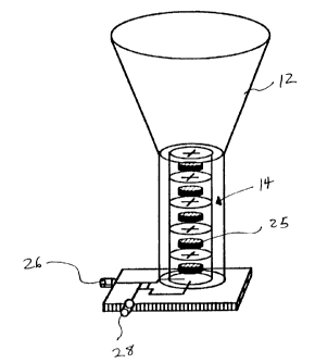
In the preferred embodiment, each radiator 12 and
its respective band pass filter 14 are integrated into the
structure shown in Figure 2. Each radiator 12 is preferably
a horn constructed of a lightweight material such as copper
plated graphite epo~y or finely machined aluminum. Both
circular, conical or square cross section inverted truncated
pyramidal shapes with features for balanced E and H plane
propagation are preferred with the band pass filter 14 formed
in the base of the horn. Band pass filter 14 comprises
several poles including a dual mode elliptical filter which
allows the horizontally and vertically polarized channels to
be launched into the radiating horn with very little loss and
enough isolation to enable dual polarization frequency
reuse. High Q dielectric resonators with high dielectric
constant (e.g., 10) can be used to reduce size and weight and
improve temperature stability. The frequency of the filter
14 is established by size of dielectric resonators 25 and to
a lesser degree by the dimension of the cavities in which
they are installed. The bandwidth and resonant mode is
established by the size and shape of the irises coupling one
cavity to another, and the horn and probes coupling the first
stage of the fiiter 14 to the MMICs 18. Radiator 12 and band
2063914
pass filter 14 advantageously support both right and left
hand polarization. While radiator 12 and filter 14 shown in
Figure 2 is configured to support both right and left hand
polarization, it should be understood by those of ordinary
skill in the art that radiator 12 and filter 14 may be
modified to support either only left hand polarization or
only right hand polarization. Depending on the polarization
desired, the appropriate output 26, 28 from filter 14 is
coupled to the respective test coupler 16 and MMIC 18. To
support both left and right hand polarization a test coupler
16 and MMIC 18 are needed for each output 26, 28.
In an alternate embodiment, each radiator 12 may
comprise a patch array as shown in Figure 3. Figure 3
illustrates an e~ploded view of a low profile array feed
cluster cell 30. The alternate embodiment of radiator 12,
cluster cell 30, has four elements and comprises a first
layer of radiating patch elements 32, a second layer of
radiating patch elements 34, a layer of coupling slots 36 and
a power distribution network 38. First layer of radiatins
patch elements 32 is placed in a parallei plane above second
layer of radiating patch elements 34. Both the first and
second layers 32, 34 are placed in a parallel plane above
layer of coupling slots 36. Finally, these three layers 32,
34 and 36 are positioned above power distribution network 38.
The structure of the distribution network 38 establishes the
polari2ations launched from the patches. The signals to and
from cluster cell 30 are then output bv power distribution
2063914
network 38 through band pass filter 14 to test coupler 16.
As with the preferred embodiment, a plurality of cluster
cells 30 each having a respective band pass filter 14 is used
to receive microwave signals. The patches are analogous to
the horns described above.
As shown best in Figure lA, test coupler 16 is
coupled between each band pass filter 14 and its respective
MMIC 18. Each test coupler 16 is constructed in strip line.
A Lange coupler or unbalanced resistive divider may be used.
Each test coupler 16 is also coupled to calibration circuit
22. Test couplers 16 allow measurement of the incoming
signal at each beam or radiator 12. Test couplers 16 also
permit a calibrated test signal to be input into the
respective MMIC 18 and through the other circuitry such as
stripline combiner 20, and ~ammer detector and correlator 24
to test all primary signal paths or detect jammers in the
geographical region illuminated by each respective radiator
12.
The output of each test coupler 16 is coupled to
the input of a MMIC 18. The present invention provides a
dedicated MMIC 18 for each radiator 12 to establish the noise
figure, phase and amplitude of the channel before the loss
embodied in the combining network to improve system
sensitivity 12. Each MMIC 18 is a monolithic microwave
integrated circu-t including a low noise ampl-fier, mi~.er IF
amplifier, and phase shifter. The MMICs 18 are co-located
with a contrcller 7~ that c-ntains a universa synchr~nous
- 10 -
2063914
asynchronous receiver/transmitter (USART), digital to analog
converters, a microprocessor, buffers and memory. The MMICs
18 amplify, frequency convert, phase shift and attenuate the
input signal in response to control signals sent to the MMIC
18. Each controller 73 has inputs for receiving control
signals. The present invention also couples each MMIC 18 to
receive a local oscillator signal from a stripline splitter
40.
The present invention also includes a control bus
42 for sending control signals to each MMIC 18, calibration
circuit 22 and jammer detector and correlator 24. Control
bus 42 is coupled to the control inputs of all 61 MMICs 18,
as well as the control inputs of calibration circuit 22 and
jammer detector and correlator 24. In the preferred
embodiment, control bus 42 is also coupled to a computer (not
shown) that provides digital signals to control the
amplification, attenuation and phase shift performed by each
MMIC 18. Control bus 42 is preferably a planar pattern of
leads interconnecting MMICs 18. This planar pattern of leads
in a ribbon like structure permits the conductors to pass
under all MMICs with only one or two layer of etched copper.
Each MMIC 18 has a unique address determined by a pattern of
open or shorted connections to ground. All the commands
travel along control bus 9, to all MMICs 18. Each individual
MMIC 18 is able to determine if it ic the intended recipient
of the control signal by comparing the address of the command
signal to the pattern of open and shorted connections for a
2063919
match. If there is no match the particular MMIC 18 ignores
the signal on control bus 42. On the other hand, if there is
a match in between the address of MMIC 18 and the command
signal on control bus 42 then MMIC 18 executes the command
signal by modifying the signal received from its respective
radiators 12. Thus, the present invention provides a
plurality of MMICs 18 each of which is independently
controllable to amplify and nullify signals from radiators 12
thereby allowing areas of interest in the antenna feed 10 to
be focused upon.
The output of each MMIC 18 is coupled to a
respective input on stripline power combiner 20. In the
preferred embodiment, stripline combiner 20 has 61 inputs and
a single output. Stripline combiner 20 forms a composite
signal from all 51 signals input by MMICs 18. The output of
stripline combiner 20 is coupled to a lead 44 that provides
the output of the present invention with the desired pattern
coverage.
Another test coupler 46 is also coupled to the
output of stripline combiner 20. Test coupler 46 passes the
signal from stripline combiner 20 to the output of the
present invention and also provides the output of stripline
combiner 20 to jammer detector and correlator 24.
Jammer detector and correlator 24 preferably
includes a MMIC ~0, a correlatlon processor 52, analoa to
digital converters 54, ampllfiers 56 and 66, power splitter
58, phase detec~ors 60, integrators 62, and a hybrid 64.
2063914
Jammer detector and correlator 24 receives signals from each
individual radiator 12 via coupler 16 and switches 76 and
78. These signals are amplified by amplifier 66 and coupled
to MMIC 50. The output of MMIC 50 is applied to a 90 degree
hybrid 64 which drives the pair of phase detectors 60. The
second input to each of the phase detectors 60 is derived
from the output of combiner 20 via coupler 46. The phase
detector 60 outputs are coupled to integrators 62. The
signals from integrators 62 are converted to digital streams
by the analog to digital converters 54 and applied to the
correlation processor 52. As illustrated in Figure 1, MMIC
50 is also coupled to control bus 42 to receive control
signals and return data. MMIC 50 is also coupled to the
system local oscillator input on line 72 by a coupler 70.
Coupler 70 provides the system local oscillator input signal
to MMIC 50 and stripline splitter 40.
The calibration circuit 22 preferably includes a
calibration signal generator 74, a switch and bus interface
76 and a calibration switch 78. Signal generator 74,
interface 76 and calibration switch 78 are coupled to control
bus 42 to receive control signals. The sianal generator 74
produces and outputs a test signal for testing the setting of
the MMICs 18. The output of signal generator 74 is also
coupled to calibration switch 78. Calibration switch 78 is
coupled to the input of jammer detector and correlator 24.
Thus, depending on the position of calibration switch 78
there is either a path between slgn21 ger.erator 74 and
20639~4
interface 76, or between correlator 24 and interface 76.
Interface 76 is preferably a 64 to 1 test switch and bus
interface, and coupled to the 61 test couplers 16 dedicated
to radiators 12, respectively. Interface 76 selectively
couples calibration switch 78 to one of the 61 test couplers
16 in response to control signal on control bus 42.
Therefore, bus interface 76 and calibration switch 78 may be
positioned to send a test signal from signal generator 74 to
any one of the 61 test couplers 16, and its respective MMIC
18 and radiator 12. In the alternative, bus interface 76 and
calibration switch 78 may be positioned to send the signal
received by any one of the 61 radiators 12 and its respective
band pass filter 14 to correlator 24 for comparison with the
composite output signal on line 44.
Referring now to Figure 4 and 5, the integrated
single package forming antenna feed and beam forming network
10 of the present invention is illustrated. Figure 4 shows a
perspective view of a preferred embodiment with the pluralitv
of radiators or horns 12. Most of the remaining portions of
the present invention are constructed in the layers
supporting the plurality of radiators 12. The present
invention advantageously reduces the size and weight of
antenna feed and beam forming network 10 by constructing the
stripline combiner 20r calibration circuit 22, and correlator
24 with a beamforming netwcrk 80. Ac noted above, the
preferred embodiment of the present invention supports both
left and right hand circular polari-ation. The
- 14 -
2063914
cross-sectional side view of Figure 5 illustrates antenna
feed and beam forming network 10 with two sets of MMICs 18
and beamforming networks 80 (one for each polarization). As
shown in Figure 5, beamforming networks 80 have calibration
circuit 22 placed on the top layer and MMICs placed on the
bottom layers. Each beam forming network 80 is comprised of
several layers of circuitry including (from top to bottom) a
calibration and aperture reuse switch layer, a ground plane,
a calibration and aperture reuse switch interconnect layer, a
ground plane, a control distribution interconnect layer, a
control distribution layer, a ground plane, a L.O.
distribution interconnect layer a ground plane, a L.O.
distribution layer, a ground plane, a combiner interconnect
layer, a ground plane, and a combiner layer.
As shown in Figure 6, the RF combiner layer is a
series of interconnected stripline 2 to 1 combiners.
As shown in Figure 7, the L.O. Distribution layer
is a series interconnected stripline 1 tG 2 dividers.
Figure 8 illustrates a preferred layout for MMICs
18 of the present invention. Each MMIC 18 has similar
semiconductor chip packaging and is mounted to the beam
forming layers 80 by semi-rigid coaxial cable and solder
points.
Figure 9 illustrates the calibration switch layer.
The calibration switch 78 is preferabli a sin~le pole double
throw ~oltage controlled MMIC switch.
2063914
Referring now to Figures lO and 11, an alternate
embodiment of the present invention is shown. In the
alternate embodiment, the radiators 12 are formed from patch
arrays as described with reference to Figure 3. As shown in
Figure lO, each radiator consists of si~ layers. The bottom
or first layer 90 contains the exciter that provides
quadrature excitation which is in line with the crossed slots
in a ne~t layer 92. The second layer 92 is preferably copper
clad. A third layer 94 provides the necessary spacing
between the radiation e~citation layer 90 and the first
copper radiating patch 98 on a fourth layer 96. A spacer is
used for a fifth layer 100 that separates the second
radiating copper patch 102 from the first copper patch 98.
The radiators 12 are positioned in a planar array
as shown in Figure 11. Below the array, there are a series
of layers that form the beamforming network. For each of the
individual patches, the first si~. layers are as described in
Figure 10. The ne.-.t four layers are made up of the necessary
hybrids, band pass filters, amplifiers and phase shifters
required for dual polarization operation with a phased array.
The above description is intended to illustrate the
operation of the preferred embodiments and is not meant to
limit the scope of the invention. The scope of the invention
is to be delimited only by the following claims. From the
above discussion, many variations will be apparent to one
skilled in the art that would yet be encompassed by the true
spirit and scope of the invention.
- 16 -