Note: Descriptions are shown in the official language in which they were submitted.
2~6397~
CIRCUIT BYPASS DEVICE
DESCRIPTION
This is a subject invention under U.S. Government
contract # NAS3-25082. As such the Government has rights
therein.
1. Technical Field
lU
This invention relates to electrical switches and
particularly to those switches that provide conductive
shunts across circuit terminals.
2. Background Art
Unlike electrical fuses or circuit breakers
electrical. shunts provide a conductive path between
terminals in a circuit. Typically shunts provide such
paths upon the occurrence of certain triggering events.
Shunts are useful for instance in bypassing faulty battery
cells that are connected serially in power systems. In
such systems, overall system failure can result from a
single-cell failure. Such failure occurs when a cell
becomes non-conductive due to an open circuit. To bypass
the faulty cell a shunt switch is connected in parallel to
the terminals of the cell. This connection permits current
2~~~97°~
to flow around 'the cell. In space-borne systems, highly
reliable shunt mechanisms for bypassing faulty cells are
desirable. This is because power supplies are critical for
operating such systems and any repair of the supplies is
virtually impossible.
Previously electromechanical switches were
employed to bypass faulty cells. These switches were
spring-loaded and triggered by fuses. In addition other
types of switches were used for non-bypassing
applications. These other switches employed various forms
of triggering mechanisms. In particular certain other
switches were triggered by so-called heat-to-recover (HTR)
shape memory metal alloy elements. HTR elements change
shape in response to thermal increase. Such thermal
increase may be induced by current flow through the element.
Switches that employ HTR elements however
function as electrical .fuses, not shunts. U.S. Patent No.
4,700,259 to Stokes discloses an electrical. circuit
breaking device. The device breaks a conductor tensively
in response to applied current. Soviet Union Patent No.
672674 to Korobov discloses a fuse. The fuse causes an
open circuit by changing shape when heated. Current is
applied to heat the fuse. U.S. Fatent No. 4,473,859 to
Stone et al. discloses a piezoelectric circuit breaker with
a bender. The bender responds to voltage changes by
deflecting. The deflection then creates an open circuit.
- 2 -
U.S. Patent No. 4,490,975 to Yaeaer et al
discloses a self-protecting and conditioning memory metal
actuator. The actuator uses a shape-memory spring that
contracts due to temperature change. Current flow causes
the temperature to change. U.S. Patent No. 4,524,343 to
Morgan e~ discloses a self-regulated spring which
operates an actuator. The actuator functions in a
circuit-breaking application. U.S. Patent No. 4,825,184 to
Bloch et al. discloses a current-cantrolled inductor. The
inductor coil is made of shape memory alloy.
U.S. Patent No. 3,573,550 to Baker discloses an
automatically--resetting transient protection device. The
device employs diodes connected to a power supply. The
diodes serve to clamp the supply voltage at a certain level.
DISCLOSURE OF INVENTION
A circuit bypass device (30) having terminals
(70, 80) is connected to contacts (70, 80) of a cell (20)
to provide a conductive path (40) in response to voltage
e:,cursion therebetween. Device (30) comprises:
switching means (40), coupled to contacts
(70, 80), having a conductive shunt (41, 42) 'that is
- 3 -
movable from a normally non-conductive position to a
conductive position between terminals (70, 80);
detecting means (50), coupled to switching means
(40) and to contacts (70, 80), for sensing voltage
excursion beyond a specified limit between contacts
(70, 80); and
actuating means (60) coupled to switching means
(40), having a heat-to-recover shape memory metal alloy
that is formed to contract in response to detecting means
(50) sensing voltage excursion, for moving conductive shunt
(41, 92) from the non-conductive position to the conductive
position.
BRIEF DESCRIPTTON OF THE DRAWINGS
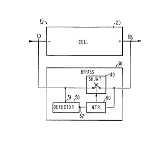
FIG. 1 is a block diagram of a battery system
10. System 10 is shown :with a cell 20 and a bypass device
30 coupled at terminals 70, 80.
FIG. 2 is a schematic diagram of a detector 50.
Detector 50 is included in bypass device 30 of FIG. 1.
FIGS. 3 and 4 are diagrams of a bypass device
31. Bypass device 31 is shown with an HTR element 61,
61'. HTR element ol, 6i' contracts translationally to move
- 4 -
2fl~3~~~
a linear shunt 41, 41' from an open condition to a close
condition. FIG. 3 shows the open condition, and FIG. 4
shows the close condition.
FIGS. 5 and 6 are diagrams of a bypass device
32. Device 32 in one diagram is shown rotatably offset by
90 degrees from device 32 as shown in the other diagram.
Device 32 is configured with an HTR element 62. HTR
element 62ocontracts torsionally to move a rotational shunt
42 rotatably. This movement provides a conductive path
between detents 176 and detents 186. Detents 176 are shown
in FIG. 5, and detents 186 are shown in FIG. 6.
FIG. 7 shows a flattened view of the outer
surface of rotational shunt 42. Angular displacements of
rotational shunt 42 about line A~-A of FIG. 5 are also
shown.
BEST MODE OF CARRYING OUT THE INVENTION
zo
In FIG. 1 a block diagram shows a power supply or
battery system 10. System 10 comprises a battery or a cell
and a circuit bypass device 30 which are coupled at
electrical contacts or terminals 70, 80. Cell 20 is
connected to system 10 with terminal 70 being designated
negatively (-) and terminal 80 being designated
positively (+). Cell 20 may be a single cell or a
_ 5 _
combination of multiple cells. Such multiple cells may be
arranged serially or in parallel with each other.
Sometirnes power supplies such as cell 20 are
subject to electrical discontinuities or open circuit
failures. Accordingly system 10 couples device 30 in
parallel to cell 20. This coupling provides a conductive
electrical switch or shunt 40 between terminals 70, 80. In
the event of an open circuit failure in cell 20 a
low-resistance bypass path is created between terminals 70,
80. Cell 20 may be manifested by any electrical circuit
requiring uninterrupted conduction between two nodes in the
circuit.
When device 30 is coupled initially to cell 20,
shunt 40 is set open. Only negligible leakage current
flows through diodes 53 and 54 as discussed later. Upon
detection of an open circuit failure in cell 20, shunt 40
is triggered to switch selectively into a close position.
Detection of the open circuit is accomplished by a detector
50. Detector 50 is coupled between terminals 70, 80 to
sense the failures therebetween.
Detector 50 is shown in FIG, 2. Detector 50
provides a conductive path between detector nodes 51, 52
when a voltage, V~, applied between nodes 51, 52 exceeds
specified limits. Detector 50 includes a plurality of
- 6 -
diodes 53, 54. These diodes 53, 54 are arranged serially
between nodes 51, 52. Node 51 is connected to terminal 70,
and node 52 is connected to heat-to-recover element (HTR)
60. 1-ITR FO is connected to shunt 40, which is then
connected to terminal 80.
The specified limits for Vp vary depending on the
direction of current flow through detector S0. In the
charge direction from node 51 to node 52, current flows
through single diode 53 when Vp exceeds a 0.5 volt limit.
This specified limit represents about one threshold drop.
In the discharge direction from node 52 to node 51, current
flows through three diodes 54 when Vp exceeds a 1.5 volt
limit. This specified limit represents about three
threshold drops. Negligible leaJcage current through diodes
53, 54 flows between nodes 51, 52 when Vp does not exceed
the specified limits.
When the polarity of cell 20 is reversed,
terminal 70 is designated positively (+) and terminal 80 is
designated negatively (-). with these designations
detector 50 is assembled with diodes 53, 54 connected in
the reverse direction. In addition cell 20 may be
assembled having a different number of diodes 53, 59. The
accumulated threshold drops of diodes 53, 54 in a given
direction correspond with the amount of Vp that is
anticipated to be applied to detector 50 in a given system
10. Nloreover for
_ 7 _
most shunting applications, 1N3164-type diodes suffice as
diodes 53, 54, The current ratings of the 1N3164-type
diodes 53, 54 are based primarily on peak transient current
rather than on continuous steady-state current.
When system 10 is operating, an open circuit
failure may occur in cell 20. Tf various external current
sources or voltage sources are coupled to cell 20 through
terminals 70, 80 the current or voltage from these external
sources is applied to device 30 at terminals 70, 80. In
particular the voltage that is applied e:;ternally at
terminals 70, 80 is applied internally as well at nodes 51,
52 of detector 50. This internal voltage application is
due to detector 50, HTR 60, and shunt 40 being connected
serially. If the voltage applied at nodes 51, 52 exceeds
specified Vp limits, current flows through detector 50.
Current flowing through detects or 50 also flows
through HTR 60, shunt 40, and terminal 80. HTR 60 is made
of heat-to-recover shape memory metal alloy. In accordance
with an important aspect of the present invention, HTR 60
functions as an actuator to move shunt 40 into a conducting
position between terminals 70, 80 in response to a voltage
e::cursion detected therebetween.
If heated sufficiently by the electrical power
dissipation of the current flowing through HTR 60, HTR 60
_ g _
contracts to bias shunt 40 into a close position. Joule
heating occurs as a function of IZR, where I is the current
in amperes flowing through HTR 60 and R is the resistance
in ohms of HTR 60. Once shunt 40 is switched into a close
position, a low-resistance, conductive path is formed
between terminals 70, 80. Consequently voltage that is
applied at nodes 51, 52 is reduced. Moreover Vp returns to
within the specified limits. This voltage reduction causes
current flowing through detector 50 and HTR 60 to stop
flowing.
HTR 60 is formed preferably into a spring shape.
This shape permits translational and torsional contraction
of the HTR 60 metal alloy, HTR 60 may also be formed into
non-spring shapes that are linearly and rotationally
stretchable. One type of non-spring shape is a so-called
torque tube. A torque tube comprises an empty cylinder
having diagonal slot openings disposed longitudinally along
the cylinder surface. HTR 60 may also be assembled from a
combination of multiple stretchable elements. Such
multiple elements may be attached serially or in parallel
to each other to improve the biasing of shunt 40.
Non-stretchable shapes of HTR 60 exhibit lesser contraction
in response to thermal increases.
The metal alloy of HTR o0 is capable of
"remembering" its initially fabricated or pre-formed
- 9 -
~~~~~~'~l
shape. When heated above a transformation temperature,
TM_A, the HTR 60 alloy transitions from a martensitic state
to an austenitic state. When austenitic HTR 60 recovers
its initial physical dimensions. While martensitic the HTR
60 alloy is characteristically soft and malleable. Thus an
HTR 60 spring in the martensitic state stretches easily and
does not apply significant translational or torsional force
to bias shunt 40.
If sufficient current is passed through HTR 60 it
becomes heated to temperatures above TM_a. At these
temperatures the HTR 60 alloy becomes austenitic. When
austenitic the HTR 60 spring hardens and contracts to
return to its unstretched, original dimensions. During
this contraction considerable force is applied by HTR 60 to
bias shunt 90 rapidly into a close switch position.
Biasing is accomplished torsionally and translationally.
Since current stops flowing throw gh HTR 60 upon the closing
of shunt 40, HTR 60 cools to a temperature below TM_A. As a
result of HTR 60 cooling, the force applied to bias shunt
90 becomes insignificant once again.
The HTR 60 alloy is composed primarily of nickel
and titanium. One such alloy may be obtained from Raychem
Corporation in a (45-52%) nickel, (35-40%) titanium,
(10-15%) niobium composition. This composition includes
about 1-2% of other constituents. Moreover for this
- 10 -
2a~39'~'~
composition, TM~A is approximately 175° C. However TM_A
varies depending on the particular composition.
In summary three conductive paths are possible
between terminals 70, 80. The first path is through cell
20. This path is available when cell 20 is functioning
properly and not subject to an open circuit failure.
However if an open circuit failure occurs in cell 20 then
current flows through a second path. This path is through
detector 50, HTR 60, and shunt 40. The second path is
available only while Vp erceeds specified limits and shunt
90 is set open. Finally once shunt 40 is switched into a
close position, a third path is enabled through shunt 40.
Detector 50 may be triggered remotely. Remote
triggering allows detector 50 to detect a false open
circuit condition and permits cell 20 to be bypassed
selectively even if cell 20 is non-faulty. This type of
bypassing might be desirable to preempt an anticipated open
circuit failure. Remote triggering is accomplished by
applying a voltage to terminals 70, 80 or nodes 51, 52 in
an amount which is sufficient to cause Vp excursion outside
the specified limits.
After device 30 is triggered to switch shunt 40
into a close position, device 30 may be reset to reopen
shunt 40. This resetting is performed much like a
- 11 --
conventional circuit breaker might be reset. To reset
device 30, HTR 60 is cooled to a temperature sufficiently
below a second transformation temperature, TAM. At TA_~ the
HTR 60 alloy transitions back to the martensitic state from
the austenitic state. When HTR 60 is martensitic, shunt 40
is returned mechanically to its initial open position.
Like T~_A, TA_M varies with alloy composition. For the
described Raychem alloy composition, TA_M is approximately
-30° C. Cooling is achieved by applying a coolant such as
freon or liquid nitrogen directly onto HTR 60.
FIGS. 3 and 4 illustrate a bypass device 31 that
is configured with a translationally-contracting HTR 61,
61'. HTR 61 represents HTR element 60 in a stretched
condition, and HTR 61' represents HTR element 60 in a
contracted condition, In FIG. 3 device 31 is shown with a
linear shunt 41 which is in an open condition. In FIG. 4
device 31 is shown with linear shunt 41' which is in a
close condition. Terminals 71, $1 of device 31 are coupled
respectively to terminals 70, 80 of cell 20. Device 31 is
assembled in a case 97.. Case 91 provides thermal
insulation that is adequate to prevent transient external
heat sources from raising the temperature therein to TM_A.
Device 31 is assembled with terminal 71 connected
to detector 50 at node 51. Detector 50 is also connected
at node 52 to HTR 61. Shunt 41 and HTR 61 are connected as
- 12 -
well. HTR 61 is stretched translationally between detector
50 and shunt 41. Since HTR 61 is martensitic when
assembled initially in device 31, HTR 61 ererts
insignificant force on shunt 41. Shunt 41 is connected to
terminal 81 through detests 86 which hold shunt 41 .in place
at indentation 47. Detests 86 apply inward force to
maintain electrical contact to shunt 41 through resilient
prongs 88 e:a ended from terminal 81.
When detector 50 senses an open circuit failure
HTR 61 is caused by detector 50 to contract
translationally. This contraction causes shunt 41' to be
pulled into a close position as shown in FIG. 4. As shunt
41' is biased to move toward terminal 71, detests 86 are
disengaged from indentation 47 and then re-engaged at
indentation 48. Detests 76 are pushed 'toward terminal 81
to slide up ramp 45 on shunt 41'. When pushed beyond ramp
45, detests 76 become engaged at indentation 46. Detests
76 apply inward force to maintain electrical contact to
shunt 41'~through resilient prongs 89 eVtended from
terminal 71.
Shunt 41, 41' is constructed of conductive
material such as copper to provide low-resistance
conduction between terminals 71, 81. To ensure that
detests 76 are well-seated in indentations 46, ramp 45 is
surface-coated with an electrical insulator such as
- 13 -
fiberglass, ceramic, or polyimide. This insulation
prevents detent.s 76 from engaging shunt 41' conductively
before detents 76 are well-seated in indentations 46. In
particular this insulation prevents HTR 61' from cooling
prematurely and uncontracting before shunt 41' is switched
completely into a close position.
In FIGS. 5 and 6 an alternative bypass device 32
is illustrated. Device 32 is configured with a
torsionally-contracting HTR 62 and a contactor barrel or
rotational shunt 42. Shunt 42 is movable torsionally to
provide electrical conductivity between terminals 72, 82.
In comparison to device 31, device 32 is potentially more
compact since it does not require the additional
longitudinal space that device 31 requires between
terminals 71, 81. As described earlier such additional
longitudinal space serves to permit translational movement
of linear shunt 41.
In FIG. 5 terminal 72 is shown connected to
detents 176 through resilient prongs 189. Prongs 189 apply
inward force to maintain electrical contact against the
outer surface of shunt 42. In FIG. 5 device 32 is shown
rot atably offset by 90 degrees from device 32 shown in FIG.
6. Terminal 82 is also shown connected to detents 186
through resilient prongs 188. Similarly to prongs 18a,
prongs 188 apply inward force to maintain electrical
- 14 -
2~6~~~11
contact against the outer surface of shunt 42. Terminals
72, 82 of device 32 are coupled respectively to terminals
70, 80 of cell 20. Device 32 is assembled in a case 92.
Case 92 provides thermal insulation that is adequate to
prevent transient ea ernal heat sources from raising the
temperature therein to TM_A.
Device 32 is assembled with terminal 72 connected
to detector 50 at node 51. Detector 50 is also connected
at node 52 to HTR 62. In addition HTR 62 is connected to
shunt 42. Shunt 42 is shown in FIG. 7 in a flattened
view. The view indicates angular displacements about line
A-A as shown in FIG. 5. Shunt 42 is cylindrical and
includes on its outer surface insulating sections 145 and
conductive strips 146, 197, 148. Strips 146, 147, 148 are
manufactured with conductive material such as copper.
Sections 145 are manufactured with insulating material such
as fiberglass, polyimide, or ceramic. Shunt 42 is mounted
rotatably on a non-conducting pivot pin 100 coupled to
terminal 82.
Strip 148 is wrapped continuously, i.e., 360
degrees, around the outer surface of shunt 42. Thus when
shunt 42 rotates, detents 186 engage strip 148
continuously. Strips 147 connect strips 148, 146. Strips
146 are positioned discontinuously around the outer surface
of shunt 42. Thus when shunt. 42 ratates, electrical
- 15 -
conductivity between terminals 72, 82 is provided when
detents 176 conductively engage strips 146. However such
conductivity is interrupted when detents 176 engage
sections 145.
4~~hen device 32 is coupled initially to cell 20,
HTR 62 is twisted or deformed torsionally between detector
50 and shunt 42. Since HTR 62 is martensitic when
assembled initially in device 32, HTR 62 exerts
insignificant force on shunt 42. Also shunt 42 is set open
initially by aligning detents 176 not to engage strips 146
conductively. Indentations may be placed on the outer
surface of shunt 42 coinciding with strips 146 and sections
145. These indentations permit detents 176 to engage shunt
42. more securely.
When detector 50 senses an open circuit failure,
detector 50 causes HTR 62 to contract torsionally. This
contraction applies a torsional force to shunt 42. As a
result of this torsional force, shunt 42 is displaced
angularly about line A-A as shown in FIG. 5. Furthermore
this displacement aligns detents 176 and strips 146 to
contact each other. Such contact serves to provide
conduction between terminals 72, 82.
Additional strips 147, 146 may be interspersed on
shunt 42. These additional strips 147, 146 provide more
- 16 -
~063~~~
conduction points against which detents 176 may be
aligned. Since additional strips 147, 146 reduce the
angular displacement of shunt 42 that is necessary to
provide conduction between strips 146 and detents 176,
faster switching of device 32 is achieved.
15
25
- 17 -
0