Language selection

Search

Patent 2063984 Summary

Third-party information liability

Some of the information on this Web page has been provided by external sources. The Government of Canada is not responsible for the accuracy, reliability or currency of the information supplied by external sources. Users wishing to rely upon this information should consult directly with the source of the information. Content provided by external sources is not subject to official languages, privacy and accessibility requirements.

Claims and Abstract availability

Any discrepancies in the text and image of the Claims and Abstract are due to differing posting times. Text of the Claims and Abstract are posted:

  • At the time the application is open to public inspection;
  • At the time of issue of the patent (grant).
(12) Patent: (11) CA 2063984
(54) English Title: SYSTEM FOR PREVENTING ABNORMAL HEATING OF THERMAL HEAD
(54) French Title: SYSTEME DE PREVENTION DE L'ECHAUFFEMENT ANORMAL DE TETES THERMIQUES
Status: Deemed expired
Bibliographic Data
(51) International Patent Classification (IPC):
  • B41J 2/365 (2006.01)
  • B41J 2/375 (2006.01)
(72) Inventors :
  • NAKANO, AKIRA (Japan)
  • AMENO, KEIJI (Japan)
(73) Owners :
  • KABUSHIKI KAISHA TOSHIBA (Not Available)
(71) Applicants :
(74) Agent: MARKS & CLERK
(74) Associate agent:
(45) Issued: 1997-09-09
(22) Filed Date: 1992-03-25
(41) Open to Public Inspection: 1992-09-27
Examination requested: 1992-03-25
Availability of licence: N/A
(25) Language of filing: English

Patent Cooperation Treaty (PCT): No

(30) Application Priority Data:
Application No. Country/Territory Date
84,555/1991 Japan 1991-03-26

Abstracts

English Abstract


A system for preventing abnormal heating of a thermal
head, which is configured with pure hardware. In the system,
when a temperature of the thermal head becomes an abnormally
high temperature exceeding a predetermined temperature and/or
an active time of a print-time setting signal cyclically
issued from a microcomputer for activating the thermal head
only for a time period necessary for printing of one line of
picture image becomes abnormally long, a flip-flop is set so
that three sorts of switch circuits are respectively operated
in such a manner as follows, whereby the abnormal heating of
the thermal head can be prevented at a very high reliability.
(1) The supply of a drive voltage to the thermal head for
heating the thermal head is forcibly stopped.
(2) The input of the print-time setting signal to the
thermal head is forcibly stopped.
(3) A picture image signal supplied from the
microcomputer to the thermal head is cut off and, instead of
the picture image signal from the microcomputer, a signal
indicative of a non-printing picture image, e.g., all-white
picture image, is forcibly supplied to the thermal head as the
picture image signal.


French Abstract

'invention est un système à configuration purement matérielle servant à empêcher l'échauffement excessif d'une tête thermique. Dans ce système, quand la température de la tête thermique devient anormalement élevée et dépasse une température prédéterminée et/ou quand la durée du signal de réglage de temps d'impression émis périodiquement par un micro-ordinateur pour activer la tête thermique durant la période nécessaire à l'impression d'une ligne d'image devient anormalement longue, une bascule est activée pour mettre en fonction trois circuits de commutation, dont l'effet est décrit ci-après, ce qui empêche l'échauffement anormal de la tête thermique avec une très grande fiabilité. 1) La tension d'attaque appliquée à la tête thermique pour la chauffer est supprimée. 2) La transmission à la tête thermique du signal de réglage du temps d'impression est interrompue. 3) Le signal d'imagerie fourni à la tête thermique par le micro-ordinateur est supprimé alors qu'un signal correspondant à la non-impression d'une image, plus précisément un signal correspondant à une image entièrement blanche, est fourni à la tête thermique comme signal d'imagerie.

Claims

Note: Claims are shown in the official language in which they were submitted.


THE EMBODIMENTS OF THE INVENTION IN WHICH AN EXCLUSIVE
PROPERTY OR PRIVILEGE IS CLAIMED ARE DEFINED AS FOLLOWS:
1. An abnormal heating prevention system for preventing
abnormal heating of a thermal head including a heating
resistor array arranged as associated with picture elements of
one line of a picture image, a drive voltage supply circuit
for parallelly supplying a drive voltage to each of the
heating resistors, a shift register for serially receiving a
picture image signal from a printing control microcomputer
through a first signal line on the basis of a shift clock
received from the microcomputer through a second signal line,
a latch circuit for parallelly collectively latching the
picture image signal of one line on the basis of a latch clock
received from the microcomputer through a third signal line, a
gate array for performing a logical "AND" operation of a
print-time setting signal cyclically received from the
microcomputer through a fourth signal line and the latched
picture image signal of one line to put only part of the
picture image signal indicative of black pixels in an active
state for an active time set by the print-time setting signal,
and a driver for applying the drive voltage to ones of the
heating resistors corresponding to the active part of the
picture image signal only for the active time to heat the ones
of the heating resistors, the system comprising:
a temperature detecting element mounted on the thermal
head for detecting a temperature of the thermal head to output
a voltage indicative of the detected temperature;
reference voltage output means for outputting a voltage
corresponding to a given temperature of the thermal head as a


22


reference voltage;
a comparator for comparing the output voltage of the
temperature detecting element with the reference voltage to
output a signal having a first logical level when the output
voltage of the temperature detecting element does not exceed
the reference voltage and to output a signal having a second
logical level when the output voltage of the temperature
detecting element exceeds the reference voltage;
a switch connected to the drive voltage supply circuit
for maintaining supply of the drive voltage to the heating
resistor array only during output of a power supply control
signal from the microcomputer through a fifth signal line; and
a gate connected to the fifth signal line for opening the
fifth signal line during output of the signal having the first
logical level from the comparator and for closing the fifth
signal line when the signal having the second logical level is
output from the comparator.
2. An abnormal heating prevention system as set forth in
claim 1, further comprising a gate connected to the fourth
signal line for opening the fourth signal line during the
output of the signal having the first logical level from the
comparator and for closing the fourth signal line when the
signal having the second logical level is output from the
comparator.
3. An abnormal heating prevention system as set forth in
claim 1, further comprising a gate connected to the first
signal line for opening the first signal line during the
output of the signal having the first logical level from the


23


comparator and for closing the first signal line when the
signal having the second logical level is output from the
comparator, a clock generator for generating a pseudo shift
clock that corresponds to a simulation of a shift clock issued
from the microcomputer through the second signal line and also
for generating a pseudo latch clock that corresponds to a
simulation of a latch clock issued from the microcomputer
through the third signal line, and a selector circuit
connected to the second and third signal lines for selectively
outputting the shift clock and the latch clock issued from the
microcomputer respectively to the second and third signal
lines during the output of the signal having the first logical
level from the comparator and for selectively outputting the
pseudo shift clock and the pseudo latch clock generated from
the clock generator respectively to the second and third
signal lines when the signal having the second logical level
is issued from the comparator.
4. An abnormal heating prevention system for preventing
abnormal heating of a thermal head including a heating
resistor array arranged as associated with picture elements of
one line of a picture image, a drive voltage supply circuit
for parallelly supplying a drive voltage to each of the
heating resistors, a shift register for serially receiving a
picture image signal from a printing control microcomputer
through a first signal line on the basis of a shift clock
received from the microcomputer through a second signal line,
a latch circuit for parallelly collectively latching the
picture image signal of one line on the basis of a latch clock


24


received from the microcomputer through a third signal line, a
gate array for performing a logical "AND" operation of a
print-time setting signal cyclically received from the
microcomputer through a fourth signal line and the latched
picture image signal of one line to put only part of the
picture image signal indicative of black pixels in an active
state for an active time set by the print-time setting signal,
and a driver for applying the drive voltage to ones of the
heating resistors corresponding to the active part of the
picture image signal only for the active time to heat the ones
of the heating resistors, the system comprising:
a temperature detecting element mounted on the thermal
head at a suitable position for detecting a temperature of the
thermal head to output a voltage indicative of the detected
temperature;
reference voltage output means for outputting a voltage
corresponding to a given temperature of the thermal head as a
reference voltage;
a comparator for comparing the output voltage of the
temperature detecting element with the reference voltage to
output a signal having a first logical level when the output
voltage of the temperature detecting element does not exceed
the reference voltage and to output a signal having a second
logical level when the output voltage of the temperature
detecting element exceeds the reference voltage; and
a gate connected to the fourth signal line for opening
the fourth signal line during the output of the signal having
the first logical level from the comparator and for closing


the fourth signal line when the signal having the second
logical level is issued from the comparator.
5. An abnormal heating prevention system as set forth in
claim 4, further comprising a gate connected to the first
signal line for opening the first signal line during the
output of the signal having the first logical level from the
comparator and for closing the first signal line when the
signal having the second logical level is output from the
comparator, a clock generator for generating a pseudo shift
clock that corresponds to a simulation of a shift clock issued
from the microcomputer through the second signal line and also
for generating a pseudo latch clock that corresponds to a
simulation of a latch clock issued from the microcomputer
through the third signal line, and a selector circuit
connected to the second and third signal lines for selectively
outputting the shift clock and the latch clock issued from the
microcomputer respectively to the second and third signal
lines during the output of the signal having the first logical
level from the comparator and for selectively outputting the
pseudo shift clock and the pseudo latch clock generated from
the clock generator respectively to the second and third
signal lines when the signal having the second logical level
is issued from the comparator.
6. An abnormal heating prevention system for preventing
abnormal heating of a thermal head including a heating
resistor array arranged as associated with picture elements of
one line of a picture image, a drive voltage supply circuit
for parallelly supplying a drive voltage to each of the


26


heating resistors, a shift register for serially receiving a
picture image signal from a printing control microcomputer
through a first signal line on the basis of a shift clock
received from the microcomputer through a second signal line,
a latch circuit for parallelly collectively latching the
picture image signal of one line on the basis of a latch clock
received from the microcomputer through a third signal line, a
gate array for performing a logical "AND" operation of a
print-time setting signal cyclically received from the
microcomputer through a fourth signal line and the latched
picture image signal of one line to put only part of the
picture image signal indicative of black pixels in an active
state for an active time set by the print-time setting signal,
and a driver for applying the drive voltage to ones of the
heating resistors corresponding to the active part of the
picture image signal only for the active time to heat the ones
of the heating resistors, the system comprising:
a temperature detecting element mounted on the thermal
head for detecting a temperature of the thermal head to output
a voltage indicative of the detected temperature;
reference voltage output means for outputting a voltage
corresponding to a given temperature of the thermal head as a
reference voltage;
a comparator for comparing the output voltage of the
temperature detecting element with the reference voltage to
output a signal having a first logical level when the output
voltage of the temperature detecting element does not exceed
the reference voltage and to output a signal having a second


27


logical level when the output voltage of the temperature
detecting element exceeds the reference voltage;
a gate connected to the first signal line for opening the
first signal line during the output of the signal having the
first logical level from the comparator and for closing the
first signal line when the signal having the second logical
level is issued from the comparator;
a clock generator for generating a pseudo shift clock
that corresponds to a simulation of a shift clock issued from
the microcomputer through the second signal line and also for
generating a pseudo latch clock that corresponds to a
simulation of a latch clock issued from the microcomputer
through the third signal line; and
a selector circuit connected to the second and third
signal lines for selectively outputting the shift clock and
latch clock issued from the microcomputer respectively to the
second and third signal lines during the output of the signal
having the first logical level from the comparator and for
selectively outputting the pseudo shift clock and pseudo latch
clock generated from the clock generator respectively to the
second and third signal lines when the signal having the
second logical level is issued from the comparator.
7. An abnormal heating prevention system for preventing
abnormal heating of a thermal head including a heating
resistor array arranged as associated with picture elements of
one line of a picture image. a drive voltage supply circuit
for parallelly supplying a drive voltage to each of the
heating resistors, a shift register for serially receiving a


28


picture image signal from a printing control microcomputer
through a first signal line on the basis of a shift clock
received from the microcomputer through a second signal line,
a latch circuit for parallelly collectively latching the
picture image signal of one line on the basis of a latch clock
received from the microcomputer through a third signal line, a
gate array for performing a logical "AND" operation of a
print-time setting signal cyclically received from the
microcomputer through a fourth signal line and the latched
picture image signal of one line to put only part of the
picture image signal indicative of black pixels in an active
state for an active time set by the print-time setting signal,
and a driver for applying the drive voltage to ones of the
heating resistors corresponding to the active part of the
picture image signal only for the active time to heat the ones
of the heating resistors, the system comprising:
a timer having a timer time set at a period time of the
print-time setting signal or at a time slightly larger than
the period time, for performing its time measuring operation
during the active time of the print-time setting signal, for
resetting its time measuring operation each time the
print-time setting signal becomes inactive, for outputting a
signal having a first logical level when the measured time
does not reach the timer time, and for outputting a signal
having a second logical level when the measured time reaches
the timer time;
a switch connected to the drive voltage supply circuit
for maintaining supply of the drive voltage to the heating


29


resistor array only during output of a power supply control
signal from the microcomputer through a fifth signal line; and
a gate connected to the fifth signal line for opening the
fifth signal line during output of the signal having the first
logical level from the timer and for closing the fifth signal
line when the signal having the second logical level is output
from the timer.
8. An abnormal heating prevention system as set forth in
claim 7, further comprising a gate connected to the fourth
signal line for opening the fourth signal line during the
output of the signal having the first logical level from the
timer and for closing the fourth signal line when the signal
having the second logical level is output from the timer.
9. An abnormal heating prevention system as set forth in
claim 8. wherein the timer receives the print-time setting
signal for triggering its time measuring operation and its
resetting operation from an output of the gate connected to
the fourth signal line.
10. An abnormal heating prevention system as set forth in
claim 7, further comprising a gate connected to the first
signal line for opening the first signal line during the
output of the signal having the first logical level from the
timer and for closing the first signal line when the signal
having the second logical level is output from the timer. a
clock generator for generating a pseudo shift clock that
corresponds to a simulation of a shift clock issued from the
microcomputer through the second signal line and also for
generating a pseudo latch clock that corresponds to a


simulation of a latch clock issued from the microcomputer
through the third signal line, and a selector circuit
connected to the second and third signal lines for
selectively outputting the shift clock and latch clock issued
from the microcomputer respectively to the second and third
signal lines during the output of the signal having the first
logical level from the comparator and for selectively
outputting the pseudo shift clock and pseudo latch clock
generated from the clock generator respectively to the second
and third signal lines when the signal having the second
logical level is issued from the comparator.
11. An abnormal heating prevention system for preventing
abnormal heating of a thermal head including a heating
resistor array arranged as associated with picture elements of
one line of a picture image, a drive voltage supply circuit
for parallelly supplying a drive voltage to each of the
heating resistors, a shift register for serially receiving a
picture image signal from a printing control microcomputer
through a first signal line on the basis of a shift clock
received from the microcomputer through a second signal line,
a latch circuit for parallelly collectively latching the
picture image signal of one line on the basis of a latch clock
received from the microcomputer through a third signal line, a
gate array for performing a logical "AND" operation of a
print-time setting signal cyclically received from the
microcomputer through a fourth signal line and the latched
picture image signal of one line to put only part of the
picture image signal indicative of black pixels in an active


31


~ .


state for an active time set by the print-time setting signal,
and a driver for applying the drive voltage to ones of the
heating resistors corresponding to the active part of the
picture image signal only for the active time to heat the ones
of the heating resistors, the system comprising:
a timer having a timer time set at a period time of the
print-time setting signal or at a time slightly larger than
the period time, for performing its time measuring operation
during the active time of the print-time setting signal, for
resetting its time measuring operation each time the
print-time setting signal becomes inactive, for outputting a
signal having a first logical level when the measured time
does not reach the timer time, and for outputting a signal
having a second logical level when the measured time reaches
the timer time; and
a gate connected to the fourth signal line for opening
the fourth signal line during output of the signal having the
first logical level from the timer and for closing the fourth
signal line when the signal having the second logical level is
output from the timer.
12. An abnormal heating prevention system as set forth in
claim 11, wherein the timer receives the print-time setting
signal for triggering its time measuring operation and its
resetting operation from an output of the gate connected to
the fourth signal line.
13. An abnormal heating prevention system as set forth in
claim 11, further comprising a gate connected to the first
signal line for opening the first signal line during the


32


output of the signal having the first logical level from the
timer and for closing the first signal line when the signal
having the second logical level is output from the timer, a
clock generator for generating a pseudo shift clock that
corresponds to a simulation of a shift clock issued from the
microcomputer through the second signal line and also for
generating a pseudo latch clock that corresponds to a
simulation of a latch clock issued from the microcomputer
through the third signal line, and a selector circuit
connected to the second and third signal lines for selectively
outputting the shift clock and latch clock issued from the
microcomputer respectively to the second and third signal
lines during the output of the signal having the first logical
level from the comparator and for selectively outputting the
pseudo shift clock and pseudo latch clock generated from the
clock generator respectively to the second and third signal
lines when the signal having the second logical level is
issued from the comparator.
14. An abnormal heating prevention system for preventing
abnormal heating of a thermal head including a heating
resistor array arranged as associated with picture elements of
one line of a picture image, a drive voltage supply circuit
for parallelly supplying a drive voltage to each of the
heating resistors, a shift register for serially receiving a
picture image signal from a printing control microcomputer
through a first signal line on the basis of a shift clock
received from the microcomputer through a second signal line,
a latch circuit for parallelly collectively latching the


33


picture image signal of one line on the basis of a latch clock
received from the microcomputer through a third signal line, a
gate array for performing a logical "AND" operation of a
print-time setting signal cyclically received from the
microcomputer through a fourth signal line and the latched
picture image signal of one line to put only part of the
picture image signal indicative of black pixels in an active
state for an active time set by the print-time setting signal,
and a driver for applying the drive voltage to ones of the
heating resistors corresponding to the active part of the
picture image signal only for the active time to heat the ones
of the heating resistors, the system comprising:
a temperature detecting element mounted on the thermal
head for detecting a temperature of the thermal head to output
a voltage indicative of the detected temperature;
reference voltage output means for outputting a voltage
corresponding to a given temperature of the thermal head as a
reference voltage;
a comparator for comparing the output voltage of the
temperature detecting element with the reference voltage to
output a signal having a first logical level when the output
voltage of the temperature detecting element does not exceed
the reference voltage and to output a signal having a second
logical level when the output voltage of the temperature
detecting element exceeds the reference voltage;
a timer having a timer time set at a period time of the
print-time setting signal or at a time slightly larger than
the period time. for performing its time measuring operation


34


during the active time of the print-time setting signal, for
resetting its time measuring operation each time the
print-time setting signal becomes inactive, for outputting a
signal having the first logical level when the measured time
does not reach the timer time, and for outputting a signal
having the second logical level when the measured time reaches
the timer time;
a flip-flop for outputting a signal having the first
logical level during the output of the signals having the
first logical level from the comparator and the timer and for
outputting a signal having the second logical level when the
signal having the second logical level is issued from one or
both of the comparator and the timer;
a switch connected to the drive voltage supply circuit
for maintaining supply of the drive voltage to the heating
resistor array only during output of a power supply control
signal from the microcomputer through a fifth signal line; and
a gate connected to the fifth signal line for opening the
fifth signal line during output of the signal having the first
logical level from the flip- flop and for closing the fifth
signal line when the signal having the second logical level is
output from the flip-flop.
15. An abnormal heating prevention system as set forth in
claim 14, further comprising a gate connected to the fourth
signal line for opening the fourth signal line during the
output of the signal having the first logical level from the
flip-flop and for closing the fourth signal line when the
signal having the second logical level is output from the


flip-flop.
16. An abnormal heating prevention system as set forth in
claim 15, wherein the timer receives the print-time setting
signal for trigqering its time measuring operation and its
resetting operation from an output of the gate connected to
the fourth signal line.
17. An abnormal heating prevention system as set forth in
claim 14, further comprising a gate connected to the first
signal line for opening the first signal line during the
output of the signal having the first logical level from the
flip-flop and for closing the first signal line when the
signal having the second logical level is output from the
flip-flop, a clock generator for generating a pseudo shift
clock that corresponds to a simulation of a shift clock issued
from the microcomputer through the second signal line and also
for generating a pseudo latch clock that corresponds to a
simulation of a latch clock issued from the microcomputer
through the third signal line, and a selector circuit
connected to the second and third signal lines for selectively
outputting the shift clock and latch clock issued from the
microcomputer respectively to the second and third signal
lines during the output of the signal having the first logical
level from the flip-flop and for selectively outputting the
pseudo shift clock and pseudo latch clock generated from the
clock generator respectively to the second and third signal
lines when the signal having the second logical level is
issued from the flip-flop.
18. An abnormal heating prevention system for preventing

36


abnormal heating of a thermal head including a heating
resistor array arranged as associated with picture elements of
one line of a picture image, a drive voltage supply circuit
for parallelly supplying a drive voltage to each of the
heating resistors, a shift register for serially receiving a
picture image signal from a printing control microcomputer
through a first signal line on the basis of a shift clock
received from the microcomputer through a second signal line,
a latch circuit for parallelly collectively latching the
picture image signal of one line on the basis of a latch clock
received from the microcomputer through a third signal line, a
gate array for performing a logical "AND" operation of a
print-time setting signal cyclically received from the
microcomputer through a fourth signal line and the latched
picture image signal of one line to put only part of the
picture image signal indicative of black pixels in an active
state for an active time set by the print-time setting signal,
and a driver for applying the drive voltage to ones of the
heating resistors corresponding to the active part of the
picture image signal only for the active time to heat the ones
of the heating resistors, the system comprising:
a temperature detecting element mounted on the thermal
head for detecting a temperature of the thermal head to output
a voltage indicative of the detected temperature;
reference voltage output means for outputting a voltage
corresponding to a given temperature of the thermal head as a
reference voltage;
a comparator for comparing the output voltage of the


37


temperature detecting element with the reference voltage to
output a signal having a first logical level when the output
voltage of the temperature detecting element does not exceed
the reference voltage and to output a signal having a second
logical level when the output voltage of the temperature
detecting element exceeds the reference voltage;
a timer having a timer time set at a period time of the
print-time setting signal or at a time slightly larger than
the period time, for performing its time measuring operation
during the active time of the print-time setting signal, for
resetting its time measuring operation each time the
print-time setting signal becomes inactive, for outputting a
signal having a first logical level when the measured time
does not reach the timer time, and for outputting a signal
having a second logical level when the measured time reaches
the timer time;
a flip-flop for outputting a signal having a first
logical level during the output of the signals having the
first logical level from the comparator and the timer and for
outputting a signal having a second logical level when the
signal having the second logical level is issued from one or
both of the comparator and timer; and
a gate connected to the fourth signal line for opening
the fourth signal line during output of the signal having the
first logical level from the flip-flop and for closing the
fourth signal line when the signal having the second logical
level is output from the flip-flop.
19. An abnormal heating prevention system as set forth in


38


claim 18, wherein the timer receives the print-time setting
signal for triggering its time measuring operation and its
resetting operation from an output of the gate connected to
the fourth signal line.
An abnormal heating prevention system as set forth in
claim 18, further comprising a gate connected to the first
signal line for opening the first signal line during the
output of the signal having the first logical level from the
flip-flop and for closing the first signal line when the
signal having the second logical level is output from the
flip-flop, a clock generator for generating a pseudo shift
clock that corresponds to a simulation of a shift clock issued
from the microcomputer through the second signal line and also
for generating a pseudo latch clock that corresponds to a
simulation of a latch clock issued from the microcomputer
through the third signal line, and a selector circuit
connected to the second and third signal lines for selectively
outputting the shift clock and the latch clock issued from the
microcomputer respectively to the second and third signal
lines during the output of the signal having the first logical
level from the flip-flop and for selectively outputting the
pseudo shift clock and Pseudo latch clock generated from the
clock generator respectively to the second and third signal
lines when the signal having the second logical level is
issued from the flip-flop.
21. An abnormal heating prevention system for preventing
abnormal heating of a thermal head including a heating
resistor array arranged as associated with picture elements of


39


one line of a picture image, a drive voltage supply circuit
for parallelly supplying a drive voltage to each of the
heating resistors, a shift register for serially receiving a
picture image signal from a printing control microcomputer
through a first signal line on the basis of a shift clock
received from the microcomputer through a second signal line,
a latch circuit for parallelly collectively latching the
picture image signal of one line on the basis of a latch clock
received from the microcomputer through a third signal line, a
gate array for performing a logical "AND" operation of a
print-time setting signal cyclically received from the
microcomputer through a fourth signal line and the latched
picture image signal of one line to put only part of the
picture image signal indicative of black pixels in an active
state for an active time set by the print-time setting signal,
and a driver for applying the drive voltage to ones of the
heating resistors corresponding to the active part of the
picture image signal only for the active time to heat the ones
of the heating resistors, the system comprising:
a temperature detecting element mounted on the thermal
head for detecting a temperature of the thermal head to output
a voltage indicative of the detected temperature;
reference voltage output means for outputting a voltage
corresponding to a given temperature of the thermal head as a
reference voltage;
a comparator for comparing the output voltage of the
temperature detecting element with the reference voltage to
output a signal having a first logical level when the output


voltage of the temperature detecting element does not exceed
the reference voltage and to output a signal having a second
logical level when the output voltage of the temperature
detecting element exceeds the reference voltage;
a timer having a timer time set at a period time of the
print-time setting signal or at a time slightly larger than
the period time. for performing its time measuring operation
during the active time of the print-time setting signal. for
resetting its time measuring operation each time the
print-time setting signal becomes inactive, for outputting a
signal having a first logical level when the measured time
does not reach the timer time, and for outputting a signal
having a second logical level when the measured time reaches
the timer time;
a flip-flop for outputting a signal having the first
logical level during the output of the signals having the
first logical level from the comparator and the timer and for
outputting a signal having the second logical level when the
signal having the second logical level is issued from one or
both of the comparator and the timer;
a gate connected to the first signal line for opening the
first signal line during the output of the signal having the
first logical level from the flip-flop and for closing the
first signal line when the signal having the second logical
level is output from the flip-flop;
a clock generator for generating a pseudo shift clock
that corresponds to a simulation of a shift clock issued from
the microcomputer through the second signal line and also for


41


generating a pseudo latch clock that corresponds to a
simulation of a latch clock issued from the microcomputer
through the third signal line; and
a selector circuit connected to the second and third
signal lines for selectively outputting the shift clock and
latch clock issued from the microcomputer respectively to the
second and third signal lines during the output of the signal
having the first logical level from the flip-flop and for
selectively outputting the pseudo shift clock and pseudo latch
clock generated from the clock generator respectively to the
second and third signal lines when the signal having the
second logical level is issued from the flip-flop.
22. An abnormal heating prevention system for preventing
abnormal heating of a thermal head including a heating
resistor array arranged as associated with picture elements of
one line of a picture image, a drive voltage supply circuit
for parallelly supplying a drive voltage to each of the
heating resistors, a shift register for serially receiving a
picture image signal from a printing control microcomputer
through a first signal line on the basis of a shift clock
received from the microcomputer through a second signal line,
a latch circuit for parallelly collectively latching the
picture image signal of one line on the basis of a latch clock
received from the microcomputer through a third signal line, a
gate array for performing a logical "AND" operation of a
print-time setting signal cyclically received from the
microcomputer through a fourth signal line and the latched
picture image signal of one line to put only part of the


42


picture image signal indicative of black pixels in an active
state for an active time set by the print-time setting signal,
and a driver for applying the drive voltage to ones of the
heating resistors corresponding to the active part of the
picture image signal only for the active time to heat the ones
of the heating resistors. the system comprising:
a temperature detecting element mounted on the thermal
head for detecting a temperature of the thermal head to output
a voltage indicative of the detected temperature;
reference voltage output means for outputting a voltage
corresponding to a given temperature of the thermal head as a
reference voltage;
a comparator for comparing the output voltage of the
temperature detecting element with the reference voltage to
output a signal having a first logical level when the output
voltage of the temperature detecting element does not exceed
the reference voltage and to output a signal having a second
logical level when the output voltage of the temperature
detecting element exceeds the reference voltage;
a timer having a timer time set at a period time of the
print-time setting signal or at a time slightly larger than
the period time. for performing its time measuring operation
during the active time of the print-time setting signal, for
resetting its time measuring operation each time the
print-time setting signal becomes inactive, for outputting a
signal having a first logical level when the measured time
does not reach the timer time, and for outputting a signal
having a second logical level when the measured time reaches


43


the timer time;
a flip-flop for outputting a signal having a first
logical level during the output of the signals having the
first logical level from the comparator and the timer and for
outputting a signal having a second logical level when the
signal having the second logical level is issued from one or
both of the comparator and the timer;
a switch connected to the drive voltage supply circuit
for maintaining supply of the drive voltage to the heating
resistor array only during output of a power supply control
signal from the microcomputer through a fifth signal line;
a gate connected to the fifth signal line for opening the
fifth signal line during the output of the signal having the
first logical level from the flip- flop and for closing the
fifth signal line when the signal having the second logical
level is output from the flip-flop;
a gate connected to the fourth signal line for opening
the fourth signal line during the output of the signal having
the first logical level from the flip- flop and for closing
the fourth signal line when the signal having the second
logical level is output from the flip-flop;
a gate connected to the first signal line for opening the
first signal line during the output of the signal having the
first logical level from the flip-flop and for closing the
first signal line when the signal having the second logical
level is output from the flip-flop;
a clock generator for generating a pseudo shift clock
that corresponds to a simulation of a shift clock issued from


44


the microcomputer through the second signal line and also for
generating a pseudo latch clock that corresponds to a
simulation of a latch clock issued from the microcomputer
through the third signal line; and
a selector circuit connected to the second and third
signal lines for selectively outputting the shift clock and
latch clock issued from the microcomputer respectively to the
second and third signal lines during the output of the signal
having the first logical level from the flip-flop and for
selectively outputting the pseudo shift clock and pseudo latch
clock generated from the clock generator respectively to the
second and third signal lines when the signal having the
second logical level is issued from the flip-flop.
23. An abnormal heating prevention system as set forth in
claim 22, wherein the timer receives the print-time setting
signal for triggering its time measuring operation and its
resetting operation from an output of the gate connected to
the fourth signal line.
24. An abnormal heating prevention system for preventing
abnormal heating of a thermal head, comprising:
a first detection circuit for detecting an abnormal high
temperature of a thermal head exceeding a predetermined
temperature:
a second detection circuit for detecting that an active
time of a print-time setting signal issued cyclically from a
printing control microcomputer to be active for a time period
necessary for printing of one line of a picture image becomes
abnormally long;


a stop signal output circuit, when one or both of the
first and second detection circuits detect an abnormality, for
triggering to output a recording stop signal;
a first switch circuit for forcibly stopping supply of a
drive voltage to the thermal head in response to the output of
the recording stop signal;
a second switch circuit for forcibly stopping input of
the print-time setting signal to the thermal head in response
to the output of the recording stop signal; and
a third switch circuit for cutting off supply of a
picture image signal from the microcomputer to the thermal
head in response to the output of the recording stop signal
and for forcibly supplying, instead of the picture image
signal from the microcomputer, a signal indicative of a
non-printing picture image to the thermal head as the picture
image signal.
25. An abnormal heating prevention system for preventing
abnormal heating of a thermal head. comprising:
a detection circuit for detecting an occurrence of an
abnormal heating factor in a thermal head;
a stop signal output circuit, when the detection circuit
detects the occurrence of the abnormal heating factor, for
triggering to output a recording stop signal; and
a switch circuit for forcibly putting control elements of
the thermal head in their inactive state under control of a
printing control microcomputer when the stop signal output
circuit outputs the recording stop signal.
26. An abnormal heating prevention system as set forth in


46


claim 25, wherein the detection circuit comprises one or both
of a first detection circuit for detecting an abnormal high
temperature of the thermal head exceeding a predetermined
temperature and a second detection circuit for detecting that
an active time of a print-time setting signal cyclically
issued from a printing control microcomputer to be active for
a constant time necessary for printing of one line of picture
image becomes abnormally long.
27. An abnormal heating prevention system as set forth in
claim 25, wherein the switch circuit comprises one or some of
three of a first switch circuit for forcibly stopping supply
of a drive voltage to the thermal head in response to the
output of the recording stop signal, a second switch circuit
for forcibly stopping input of the print-time setting signal
cyclically issued from the microcomputer to the thermal head
to be active for a constant time necessary for printing of one
line of picture image in response to the output of the
recording stop signal, and a third switch circuit for cutting
off the supply of a picture image signal from the microcomputer to
the thermal head in response to the output of the recording
stop signal and for forcibly supplying, instead of the picture
image signal from the microcomputer, a signal indicative of a
non-printing picture image to the thermal head as the picture
image signal.


47

Description

Note: Descriptions are shown in the official language in which they were submitted.


2063984

TITLE OF THE INVENTION


System for Preventinq Abnormal Heatinq of Thermal Head


BAC~GROUND OF THE INVENTION
1. Field of the Invention
The present invention relates to an abnormal heating
prevention system for preventin~ abnormal heating of a thermal
head used in a thermal printer and more particularly, to an
embodiment of such an abnormal heatinq prevention system which
is confiaured in the form of pure hardware to prevent the
abnormal heating of a thermal head with a high reliability.
2. Description of the Related Art
Many facsimile machines or the like have conventionally
been mounted with a thermal printer as its printing device.
Such a thermal printer has had such a problem that, since the
printer prints data on thermal sensitive paper or on ordinary
paper through ink ribbon by electrically and directly heating
an array of heating resistors of a thermal head, if an
abnormal current flows through the heating resistors, then the
thermal head per se or the recording paper is abnormally
heated, which undesirably might lead to production of fire.
As a major cause of the problem, there may be considered
that the runaway or the like of a microcomputer built in the
thermal head as a printinq controller causes a print-time
setting signal to be maintained to be continuously active
without any interruption, though the print-time setting siqnal

is set to provide a heating drive time to the heating resistor


"~, ~. ,~, ~

20639~

array for each line of picture image and is set to normally be
active for only each printinq period of the signal.
To avoid this problem, there has been proposed an
abnormal heatin~ prevention system in which switch means for
forcibly cuttins off the power supply to the heating resistors
is previously provided so as to be turned OFF when such an
abnormally long active time of the print-time settinq signal
or an abnormally hish thermal head temperature is detected,
thereby preventing the abnormal heating of the thermal head.
The prior art system, however, has a difficulty that,
since the aforementioned abnormal-heating preventing operation
is carried out under control of the aforementioned printing
control microcomputer, if a software program itself describing
the processing procedure based on the microcomputer runs away
out of control, then the above remedY becomes useless. That
is, even turning OFF the switch means becomes difficult and
the positive prevention of the abnormal heatinq of the thermal
head cannot be guaranteed.


SUMMARY OF THE IN~ENTION
In view of such circumstances, it is an object of the
present invention to provide an abnormal heating prevention
system which can positively prevent a thermal head from being
abnormally heated even when a microcomputer runs away.
In order to attain the above obiect, in accordance with a
basic aspect of the present invention, an abnormal heating
prevention system is configured in the form of pure hardware.
In accordance with a preferable aspect of the present


2~63984


invention (to be detailed later), an abnormal heatin~
prevention system comprises:
(a) first detection circuit for detectins an abnormal
hish temperature of a thermal head exceedinq a predetermined
temperature;
(b) a second detection circuit for detecting an
abnormally long active time of a print-time setting signal
issued from a microcomPUter cyclicallY so as to be active for
a time period neceSSarY for printing of one line of picture
imase;
(c) a stop signal output circuit for outputting a
recording stop signal when an abnormality is detected by one
or both of the first and second detection circuits;
(d) a first switch circuit for forcibly stoppinq supply
of a drive voltage to the thermal head in response to the
output of the recording stop signal;
(e) a second switch circuit for forcibly stopping the
input of the print-time setting signal to the thermal head in
response to the output of the recording stop signal; and
(f) a third switch circuit for interruptinq a picture
image signal supplied from the microcomputer to the thermal
head in response to the output of the recording stop signal
and for forcibly supPlying, instead of the picture image
signaI from the microcomputer, a sisnal indicative of a
non-printins picture image (e.g., all-white picture image) to
the thermal head as the picture image signal~
In more detail. the first switch circuit acts to stop the
power supply itself to the thermal head to thereby prevent the

~ ,~

~ 3


~,. ..... .. . . .
~ .

2~63984


further heating of the thermal head; the second switch circuit
acts to stop the input of the Print-time settinq signal to the
thermal head, that is, to stop the printing operation of the
thermal head to thereby prevent the further heading thereof
even when the power supply to the thermal head is maintained;
and the third switch circuit acts to allow the printing of a
non-printing picture image such as an all-white picture image,
i.e., to inhibit the substantial image printing to thereby
prevent the further heating of the thermal head, even when the
power supply to the thermal head is maintained or the
Print-time setting signal is applied to the thermal head to
put the thermal head in its printable state.
- In addition, the operation of these switch circuits
, ~ :
~ ~ depends only on the Presence or absence of the recording stop
, . ~ ~ , -
~signal~issued from th~e stop~signal output circuit and is
1ndependent~of~tbe~oper3tion of~the printing control
m~icroco~m~puter i~tself. ~ ~ .
For this reason, even w~hen the microcomPUter runs away
~or~some~reason~,~whlch leads;to~seneration of an abnormality
tha~t~the~th~ermal head is~a;bnormallY~heated to such a high
t~-mpera~tur-~exceedin~ a~predetermined level and/or tbat the
acti~ve time of the print-tlme se~tting signal becomes
abnorm311y~10ng~; the first and/or ~second detection circuit
detec~ts the~-~abnormality~,~and then~the stop s~ignal output
-circuit immediatelY outputs the recording stop signal in such
a~manner~that, regardless of~the~subsequent operation of the
micr;ocomputer~
the~fir~st~s~wit~ch~circuit stops the pOWQr supply to


,~

2~63984


the thermal head;
(2) even when such a cause as a failure in the first
switch circuit causes no realization of the stoppage of the
power supply, the second switch circuit stops the printing
operation of the thermal head; and
(3) similarly. even when such a cause as a failure in
the first and second switch circuits causes no realization of
the stoppage of the power supply or the printing operation,
the third switch circuit inhibits the substantial printing
operation of the picture image.
Since such triple overheat preventing operation is
carried out, the abnormal heating of the thermal head can be
prevented with a considerably high reliability.
With such an arrangement as mentioned above, since the
first to third switch circuits are very low in failure
probability, the present invention is not limited in practical
applications to the above example of using all the first to
third switch circuits. That is, when onlY one or two of the
flrst to third switch circuits are used. substantially the
same overheat prevention effect of the thermal head can be
realized. The system having such configuration is much
reliable compared with the prior art abnormal heatinq

~ .
prevention system which is controlled by a software through a
~ ~ ~ microcomputer.
urther, with regard to the detection circuits, so long
as at Ieast one of the above first and second detection
circuits is employed, the cause of abnormal heating can be
detected at least in the minimum level.


",~
~ 5


:~ . . . .

2063984


With an abnormal heatinc prevention system having such an
arrangement as stated above, the system can be fabricated
without involvinq siqnificant increase in cost, and
particularly when the aforementioned circuits are built in a
custom integrated circuit (IC) by new custom IC techniques,
the system can be fabricated without substantial increase in
cost.


BRIEF DESCRIPTION OF THE DR~INGS
Fig. 1 is a circuit diaqram of an entire arrangement of
an abnormal heating prevention system in accordance with an
embodiment of the present invention;
Fig. 2 is a block diagram of a detailed structure of a
thermal head part in Fig. 1;
Fig. 3 is a circuit diagram of a specific example of a
structure of a clock generator in Fiq. 1;
Fig. 4 is a timing chart for explaininq the operation of
the clock generator of Fig. 3; and
Fig. 5 is a timing chart for explaining the exemplary
operation of the system of the embodiment of Fig. 1.


DESCRIPTION OF THE PREFERRED EHBODIMENTS
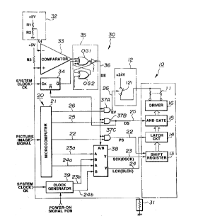
Referring first to Fig. 1, there is shown a system for
preventing abnormal heating of a thermal head in accordance
with an embodiment of the present invention.
More specifically, the system of Fig. 1 includes a

thermal head part 10 for printing data onto thermal recording
paper or ordinary paper t~rough ink ribbon, a print controller


...... .

206398~


20 having a microcomputer 21 for controlling the prin~inq
operation of the thermal head part 10 through signal lines 22,
23, 24 and 25, and an abnormal-heating preventing part 30
disposed between the thermal head Part 10 and the print
controller 20 for preventing the thermal head part 10 from
being abnormallY heated.
Explanation will first be directed to the structure of
the thermal head part 10. The detailed structure of the
thermal head part 10 is shown in Fig. 2.
As shown in Fig. 2, the thermal head part 10 includes a
heating resistor array 11 of resistors 11-1 to 11-N arranqed
to correspond in number to picture elements (pixels)
corres~o-.ding to one line of picture image, a drive voltage
supply circuit 12 for supplyinq a drive voltase of +24V to the
respective heating resistors of the heating resistor array 11,
a shift register 13 for serially receiving a picture image
signal PS from the microcomputer 21 of the print controller 20
through the signal line 22 on the basis of a shift clock (data
transfer clock) SCK received from the microcomPuter 21 through
the signal line 23 (23a), a latch circuit 14 for collectively
latching the picture image signal PS corresponding to one line
on the basis of a latch clock LCK received from the
microcomputer 21 through the signal line 24 (24a) each time

, ,
the shift register 13 stores therein the picture image signal

~- ~; PS corresponding to one line, an AND gate 15 for performing a

lo~ical "AND" oPeration of a print-time setting signal DS


~ cyclically recel~ed from the microcomputer throuqh the signal

- ~ line 25 and the latched picture image signal PS corresponding


' ~
.
.

2063984


to one line to enable only picture lmage signals ~havln~ a
logical level of "1") indicative of black pixels for a time
period that is set by the print-time setting signal and that
corresponds to a time necessary for the printing of one line
of picture imaqe, and a driver 16 for applying the drive
voltage +24V to only ones of the heating resistors 11-1 to
11-N associated with the enabled picture image signals for the
enabled time to allow them to be conductive and thus to be
heated.
~ s shown also in Fig. 1, the drive voltage supply circuit
12 comprises a switch 121 which keeps the supply of the drive
voltage +24V to the heating resistors 11-1 to 11-N durins the
reception of a power supply control signal EV from the
microcomputer 21 through a signal line 26.
Referring again to Fig. 1, the abnormal-heating
preventing part 30, which is disposed between the thermal head
part 10 and the Print controller 20 for controlling the
thermal head 10 to prevent the thermal head 10 from being
abnormally heated, comprises a thermistor 31. a reference
voltage output circuit 32 and a comparator 33 as means fo.
detecting that the thermal head 10 is heated to a high
temperature exceeding a predetermined level and also comprises
a timer 34 as means for detectins that the enable time of the
print-time setting signal DS applied to the thermal head part
10 through the signal line 25 becomes abnormally long.
In more detail, the thermistor 31 is mounted on the
thermal head part 10 at a proper location (usually, on its
wiring circuit board) to output a voltage indicative of a


:~ 8


-- . .

2~63984


temperature sensed thereby (more exactly, to decrease the
resistance of the thermistor in proportion to the temperature
to increase a current flowing therethrough , i.e., to increase
a voltage droP across a resistor R3). The reference voltage
output circuit 32 outputs, as a reference voltage Vf, a
voltage set on the basis of the output of the thermistor 31
corresponding to a temperature which is regarded as an
abnormally high temperature from experience. The comparator
33, which compares the output voltage of the thermistor 31
with the reference voltage Vf of the reference volta~e output
circuit 32, outputs a logical "H" level signal when the output
voltage of the thermistor 31 does ~ot exceed the reference
volta~e Yf and outputs a logical "L" level signal when the
output voltage of the thermistor 31 exceeds the reference

:
-v:oltage Vf.
Me~anwhile. the timer 34, which is set at a time (timer
:time~corresponding to the period time of the print-time
settins~slqnal~ DS or a time sllghtly larger than the Period
~ time~,~executes its time measuring operation during the active
s.'~ t~ime;~of~the prlnt-time~:setting signal on the basis of a system
clock:~CK~of, for~example, the associated thermal printer
(facsl;mile m~achine~ and eacb time the print-time settinq
signal DS is put in its inactive state, resets its measured
t'l-e.~ And the tlme~r 3~ ls operated to output a logical "H"
level si~nal when the measured time does not reach the timer
. , " ,
time and output a log~ical "L" level signal when the measured
t~me ~reac~hes the~tlme~r~tlme~
Th~uc . ~ when it lS det~e~ted that the thermal head part 10


i ~,"~


: ': ' , ' ' ,
: ~ ~

, ,

2063984


was heated to a high temperature exceedinq a predetermined
level and that the active time of the print-time setting
signal DS became a~normallY long, such a condition can be
judged, based on the above detected results, that the thermal
head part 10 is going into an abnormally heated state.
Accordingly, if the factors for heating the thermal head part
10 are cut off on the basis of the above judgment, it can be
prevented that the thermal head part 10 is further heated.
Such control of cutting the further heating of the thermal
head is carried out by a flip-flop 35, AND gates 37 (37A, 37B
and 37C) and a selector circuit 38, which structures and
operations will be detailed below.
First of all, the flip-flop 35, which, comprises, OR
qates OG1 and OG2 and an inverter I as shown in Fig. 1,
outputs a logical "H" level signal onto an output signal line
36 normally, i.e., when the outputs of the comparator 33 and
timer 34 are both at their logical "H" level. When either one
or both of the comparator 33 and the timer 34 outputs the
loqical "L" level signal, that is, when it is detected that
the thermal head part 10 was heated to a high temperature
exceeding the predetermined level or that the active time of
the print-time settinq signal DS became abnormally lon~; the
flip-flop 35 output a logical "L" level siqnal. For the sake
of easy explanation, the loqical "L" level signal outputted
onto the siqnal line 36 will be referred to as the "recording
stop siqnal DE", hereinafter.
The AND gate 37A, which is connected to the siqnal line
26, acts to put the siqnal line 26 in its conductive state


2063984


during the non-output of the recording stoP signal DE, i.e.,
durinq the logical "H" level time of the siqnal of the signal
line 36. whereas. to put the siqnal line 26 into its
non-conductive state when the recording stop siqnal DE is
output. During the conductive state of the siqnal line 26,
the power supply control siqnal EV issued from the
microcomputer 21 enables the power supply control of the
thermal head part 10 (the control of turning ON and OFF of the
switch 121 in the drive voltage supply circuit 12). When the
siqnal line 26 is put into the non-conductive state, however,
the switch 121 is kept at its OFF state so that the drive
signal +24V is not supplied to the thermal head part 10.
~ 'urther, the AND gate 37B, which is connected to the
signal 11ne 25, acts to put the siqnal line 25 into its
conductive state durinq the non-output of the recordinq stop
slgnal DE, whereas, to put the signal line 25 into its
non-conductive state when the recording stop signal DE is
output. During the conductive state of the signal line 25,
the print-time setting signal DS issued from the microcomputer

, : , -
21 enables the Print-time setting of the thermal head Part 10.
When the signal line 25 is put in the non-conductive state,
however, the print-time setting signal DS lS also kept in the
inactive state, which results in that the printing operation
- of the thermal head part 10 is also inhibited.
The AND gate 37C, which is connected to the signal line
22, acts to put the signal line 22 in its conductive state
du;ring the non-output of the recording stop signal DE.
whereas, to put the signal line 22 in its non-conductive state


, 11

~ ' '

206398~


when the recording stoP signal DE is output. Durin~ the
conductive state of the signal line 22, the Picture ima~e
siqnal PS issued from the microcomPuter 21 is applied to the
shift reqister 13 of the thermal head part 10. ~hen the
signal line 22 is put in the non-conductive state, howe~er,
the picture ima~e signal PS is kept fully at its inactive
level. That is, in the present embodiment, the signal PS is
tùrned into a signal representinq "white pixels", i.e., all
not-printing pixels.
Finally, the selector circuit 38, which is connected at
its output side to the signal lines 23 and 24 (terminals Y)
and also connected at its input side to signal lines 23a and
24a (terminals A) and to signal lines 23b and 24b (terminals
B), selects the signal lines 23a and 24a during the non-output
of the recording stop signal DE to apply the shift clock SCK
and the latch clock LCK issued from the microcomputer 21 to
the shift register 13 and the latch circuit 14 of the thermal
head Part 10 respectively. On the other hand, when the
recording stop siqnal DE is output, the selector circuit 38
selects the signal lines 23b and 24b to apply a pseudo ~shift
clock DSCK and a pseudo latch clock DLCK to the shift register
13 and the latch circuit 14 of the thermal head part 10

:
respectively. In this connection, the pseudo shift clock DSCK
is;~generated at a clock generator 39 based on the simulation
of the aforementioned shift clock SCK, while the pseudo latch
clock DLCK is generated at the clock generator 39 based on the
simulation of the aforementioned latch clock LCK. ~s a
result, even when the runaway or the like of the microcomputer


12
,

2063984


21 causes the stoppage of the output of the aforementioned
shift clock SCK and latch clock LCK. after the output of the
recording stop signal DE, the picture image signal to be input
to the thermal head part lO, that is, the picture image signal
to be issued from the AND gate 37C as the signal indicative of
"all white pixels" is positively sent into the thermal head
part lO under control of the pseudo shift clock DSCK and the
pseudo latch clock DLCK. It goes without saying that the "all
white pixels" are printed and the heating resistors ll-l to
ll-N will not actuallY be heated.
Fig. 3 is a specific example of the structure of the
clock generator 39 for generating the aforementioned pseudo
clocks, while Fig. 4 is a timing chart for explaining the

.
~ exemplary operation of the clock generator 39 of Fig. 3.
: ::
As shown in Fig. 3, the clock generator 39 comprises one
counter~CTi two JK~fliP-floPs FFl and FF2 and se~en AND gates
AG1 to~AG7. ~In the clock generator 39. a power-on signal PON
r~ef~er~to part~(a1 of Fig. 4) issued from the associated

,
t~hermal~;pr1nter~ (f~acsimile machine~ causes the counter CT and
; tbe~both f11p flo~Ps FF1 and ~F2 to be~ reset.~ After th1s, on
the b~as~1s~of the~sYstem clock CK (refer to Part (b) of Fig. 4
of-~the~-the~rmal prlnter (facs1m11e~mach~1ne), th~e clock
~generator 39 ~ènerates signals DC~ and D2C~ trefer to Figs.
41~) and ~ d)~fr~e~uency-div1ded~at predeterm1ned rat1os, and
OD: th~e~bas1s of these signa}s DCK and;D2CK, generates as the
pJ~eudo~sh~1~ft clock DSCK and the pseudo latch clock DLCK such

cîock~si~na1s having alter~nately an~active level as shown in
parts~(e)~and~(f) of Flg~ 4.


: ~


.

2063984


Shown in Fig. 5 is a timinq chart for explaining an
example of the operation of the embodiment of the above
arrangement~ The operation of the entire embodiment system
will be detailed below by referring also to Fig. 5.
Assume now that the thermal printer is normally oPeratins
without generating anY abnormal heating in the thermal head
part 10. Under this circumstance, the output (refer to part
(a~ of Fig. 5) of the comparàtor 33 and the outPut (refer to
part (b) of Fig. 5) of the timer 34 are both at logical "H"
level. thus the output (refer to part (c) of Fig. 5) of the
fliP-flop 35 is also at logical "H" level, whereby the AND
gates 37A to 37C are opened (to put the associated signal

.


lir.~ in the conductive statel and the selector circuit 38 is
put in~to the A-input selection mode in which the signals input
to~th~e; terminals A are selected. As a result. the embodiment

sYS~tem of~Fis~ is oPerated as follows. ~ ~
(a) The:~powe~r~supplY~control signal.EV. which~is changed
to,the~ac~ti;v~e~,s~tate (~l~osical "H";level), for~example, when the
siana~l r~ece1vin~ operatlon~ lS started~in the case of~ a
facsimile machine) or the~power is turned ON. is applied from
,the~micr~ocompu~ter;21 throu~hi~the~slsnal line'26 to th~e drive
vo~1~ta~e~'supply~circuit~l2.~s~o that~ the~switcb~121 is turned ON
to~supply~the~dri~ve voltage;~24V to~one~ends~of the heating
re~si~$to~rs 11-l,to 11-~N of~th~e ther;mal head~part 10 (refer to
pa~rts ~Id~l~ a~nd~(e) of~Fig.~5~
Ib),~The prlnt-time settln~sisnal DS~, which is issued
f,,rom the~m,icrocomP~uter 21~to~bec~ome actlv~e (losical "H" level)
,,c-yclicallY for a Predetermined time with respect to the


.

20~3984


printinq operation of each line, is aPplied to the thermal
head part 10 throu~h the signal line 25 so that the AND gate
15 is cyclically opened (in such a condition that the Picture
image siqnal indicative of black pixels causes the driver 16
to be driven) in synchronism with the timinq of the signal DS
(refer to parts (f) and (g) of Fig. 5).
(c) The picture imaqe sisnal PS, which is transferred
through the printing operation, is applied from the
microcomputer 21 throuqh the signal line 22 to the thermal
head part 10 (refer to parts (h) and (i) of Fig. ~).
(d) The shift clock (data transfer clock) SCK issued from
the microcomPuter 21 is aPPlied to the shift register 13 of
the thermal head part 10 through the signal lines 23a and 23
(refer to part (j) of Fig. 5).
(e) The latch clock LCK issued from the microcomputer 21
is applied to the latch circuit 14 of the thermal head part 10
through the signal lines 2~a and 24 (refer to part (k) of Fig.


On the other hand, the thermal head part 10 per se
repe~titively e~ecutes the followins operations (1) to (4) on
~the ~basis of these received siqnals.
(1) The picture image signal PS is serially applied to
the sh;ift register 13 in synchronism with the shift clack SCK

,,
~refer to parts (h), (i1 and'(j) of Fig. 5).
(2) In synchronism with the latch clock LCK which becomes
active when the picture image signal PS of one line is

::
~received, the picture image siqnal PS corresponding one line
pr~ev1ously stored in the shift register 13 is collectively


,

2063984


parallelly latched by the latch circuit 14 (refer to Figs. 5,
(h), (i) and (k)).
(3) The AND sate 15 performs a lo~ical "AND" of the
latched picture image signal PS of one line and the Print-time
setting signal DS to put only the Picture image signal
(logical level "1" signal) indicative of black pixels into the
active state for the time set by the print-time settins signal
DS (refer to parts (f), (g), (h) and (i) of Fig. 5).
(4) Only for the active set time, the drive voltage +24V
is applied to only ones of the heating resistors 11-1 to 11-N
corresponding to the active picture image signal (black
pixels) (put them in the conductive state) through the driver
16 to heat only the associated resistors.
During the printing operation of the thermal head Part
10, if the print-time settinq signal, which is intended to be
normally active during each printing period, is maintained to
be continuously active for some reason (refer to Parts (f) and
(g) of Fig. 5), then the occurrence of such an abnormality is
detected when the continuous active time reaches the timer
time set by the timer 34.
As already explained above, the timer 34 having the set
time corresponding to the period time.of the print-time
setting signal DS or slightly larger than the period time is
activated during the active time of the print-time setting
signal DS (output of the AND gate 37B, in the present
embodiment), i.e., at the rising edge of the Print-time
setting signal DS, whereas, the timer 34 is reset at the
falling edge of the print-time setting signal DS to thereby


16

2063984


measure the passage time on the basis of the system clock CK.
In such an example as shown in Fig. 5, when the timer 3~ is
started at the risinq edge of the print-time setting signal
DS, i.e., at a time tl and reaches the timer time without
being reset, i.e., at a time t2, the timer 34 detects that
the active time of the print-time setting signal DS became
abnormally long and outputs a logical "L" level signal ~refer
to part (b) of Fig. 5).
The output of the logical "L" level signal from the timer
34 causes the fliP-floP 35 to be set so that the flip-flop 35
outputs a logical "L" level signal as the recording stop
signal DE onto the output signal line 36 (refer to part (c) of
;Fig. 5). ,In this way, in such an embodiment system as shown
in~Fi~g.,l, w~hen the flip-fiop outputs the recording stop

,
a~ signal DE at the time t? (refer to Fig. 5). this causes all
the~AND gates~3'7A ~to~;37C to~be~closed (th~e~ass~ociated signal
nes~bein~g put in~the~non-'conductive state) so that the
selector~circ;uit 38~is~p~ut in~the B~input selection mode in
which~the sign~als lnput to,~the terminals~B are selected. after
~ wh~i~c~h~the~operation is~carried out~ln~the~fol~lowlns manner.
,'";",:,~ (A)~ Eve~n~ when~the~powe;r supply control~signal'E~ issued
rom the~microco~mputer 2I~is at~ its~active~level. the ~ND gate
37A causés~the~supplY of~the;Power~suPPlY control signàl E~ to
'thé,~,triv~é~v~oltage~supplY circuit 12 to be interrupted ~refer
to Parts-~d) and (e) of Fig. 5).
B~ EYen when~the prlnt-t~lme~settlnq signal DS issued
~,','~',','-,'f'rom the mlcrocomp,ùte~r 21~is at~ ts~acti~e level. the AND gate
~ 37B:'c;auses~the supply~of~the~p~rlnt-ti~e~setting signal DS to


'' '"": ':::'' ' ' ':


~ ', ~ ,
: ~

2063984


the thermal head part 10 (~ND gate 15) to be interrupted
(refer to parts (f) and (~) of Fig. 5).
(C) Even when the picture lmaqe signal PS is issued from
the microcomputer 21, the AND ~ate 37C causes the supply of
the siqnal PS to be interruPted and instead, a signal
indicative of "all white pixels" or "all non-printing pixels"
is sent to the thermal head part 10 (shift register 13) (refer
to Parts (h) and (i) of Fig. 5). Further, with respect to the
shift clock and the latch clock, even when the shift clock SCK
and the latch clock LCK are issued from the microcomputer 21
together with the aforementioned picture image siqnal PS, the
pseudo shift clock DSCK and the pseudo latch clock DLCK
generated from the clock qenerator 39 in Place of the above
signals are applied to the respective shift reqisters 13 and
the latch circuit 14 of the thermal head part 10 (refer to
parts (j) and (k) of Fiq. 5).
In o~ther words, the above operations (~) to (C) mean:
~ (1) The power supply to the thermal head part 10 is
:~; Dtopped~regardless of the subse~uent operation of the
microcomputer 21.
~ ~(2) Even when the above stoppage of the power supply
cannot be realized for some reasons including a failure in the
AND gate 37A or in the drive voltage supply circuit 12, the
r1n~tins operation of the thermal head part 10 is stopped
. :re~ardless of the subsequent oPeration of the microcomputer
21. ~
i3~ Even when the above stoppage of the power supply or
:the~above stoppage of the printing operation cannot be

,
:
18


"

"
- . ~. .

2063984


realized for some reasons including a failure in the AND gates
37~ and 37B or in the drive voltage supply circuit 12, the
printing operation of the Picture image is substantially
inhibited regardless of the subsequent operation of the
microcomputer 21.
In the operation (3), in particular, the heating
resistors 11-1 to 11-N of the thermal head part 10 are not
actually heated at the time of printing "all white Pixels" as
already explained above.
In this way, in accordance with the.system of the present
embodiment, since the so-called triple overheat Preventing
operation as shown in (1) to (3) is carried out, the abnormal
heating of the thermal head part 10 can be prevented at a
considerably high reliability.
The above operation has been explained in connection with
the case where the flip-flop 35 outputs the recording stop
signal DE on the basis of the detection of the abnormally long
active tim~e of the print-time setting signal DS by the timer
~34~ In this case, since the temperature of the thermal head
:part~lO is usuallY also increased when compared with the
normal time, the comParator 33 can detect the occurrence of an
::~: abnormality substantiallY in such a manner as mentioned above.
In this case,.in more detail, when the temperature of the
thermal head part 10 increases for the above reason or other
reasons, this causes the resistance value of the thermistor 31
~to be decreased so that a current flowing through the
thçrmistor 31 is increased, thus increasing the voltaqe drop
:across:the resistor R3. For this reason, when the voltage


1 9

: ~

20B3984


drop across the resistor R3 exceeds the reference voltage Vf
as the output of the reference voltage output circuit 32, the
comparator 33 outputs a lo~ical "L" level signal. The output
of the logical "L" level signal from the comparator 33 causes
the flip-flop 35 to be also set (if not set yet) so that the
flip-flop 35 outputs a logical "L" level signal as the
recording stop signal DE as in the above case (refer to part
(c) of Fiq. 5).
Since the detection of the abnormally high temperature of
the thermal head exceeding the predetermined level as well as
the detection of the abnormally long active time of the print-
time setting signal by means of the comparator 33 and the
timer 34 are carried out independentlY of their circuits,
these detections are not always performed at the same time. In
the present embodiment, since such different two sorts of
abnormality detections are parallelly carried out, an
abnormality detection accuracy can be larqely improved. In
practical applications, only one of the comparator 33 and the
timer 34 may be provided. In this case, the flip-flop 35 is
omitted and the output of the comparator 33 or the timer 34 is
connected directly to the signal line 36~
With regard to the AND gates 37A, 37B, 37C and the
selector circuit 38, since they have very low failure
probabilities, the present invention is not limited to the
aforementioned arrangement of the foregoing embodiment but in
practical applications, some of these elements maY be omitted
as necessary. Assuming that the AND gate 37A is a first
switch circuit, the AND gate 37B is a second switch circuit,


2~63984


and the AND qate 37C and the selector circuit 38 make up a
third switch circuit, then one or two of the first to third
switch circuits may be used in the present invention, in which
case substantially the same abnormal heating prevention effect
of the thermal head can be obtained as mentioned above.
With the abnormal heating prevention system having such
an arransement, when the above respective circuits are built
in an existing custom integrated circuit (IC) especially by
new custom IC techniques, the system can be fabricated without
substantially involvinq a remarkable increase in the cost.
~ lthough the clock generator 39 has been arranged as
shown in Fig. 3 to generate such pseudo shift clock DSCK and
pseudo latch clock DLCK as shown in the parts (e) and (f) of
Fig. 4 for the simplification of explanation in the foregoing
émbodiment, this is merely an example. Thus a circuit of any
arrangement may be employed so long as the circuit can send
the picture image signal PS ("all white Pixels" signal, in
this case) to the shift register 13 of the thermal head part
10 and also the sent picture imaqe si~nal PS can be latched at
the latch circuit 14 of the thermal head part 10. Of course,
the pseudo shift clock DSCK and the pseudo latch clock DLCK to
be generated from the clock generator may have substantially
the same format (timing) as the shift clock SCK and the latch
clock LCK issued from the microcomputer 21.


21

Representative Drawing
A single figure which represents the drawing illustrating the invention.
Administrative Status

For a clearer understanding of the status of the application/patent presented on this page, the site Disclaimer , as well as the definitions for Patent , Administrative Status , Maintenance Fee  and Payment History  should be consulted.

Administrative Status

Title Date
Forecasted Issue Date 1997-09-09
(22) Filed 1992-03-25
Examination Requested 1992-03-25
(41) Open to Public Inspection 1992-09-27
(45) Issued 1997-09-09
Deemed Expired 2006-03-27

Abandonment History

There is no abandonment history.

Payment History

Fee Type Anniversary Year Due Date Amount Paid Paid Date
Application Fee $0.00 1992-03-25
Registration of a document - section 124 $0.00 1992-10-09
Maintenance Fee - Application - New Act 2 1994-03-25 $100.00 1994-02-03
Maintenance Fee - Application - New Act 3 1995-03-27 $100.00 1995-01-30
Maintenance Fee - Application - New Act 4 1996-03-25 $100.00 1996-01-08
Maintenance Fee - Application - New Act 5 1997-03-25 $150.00 1997-01-14
Final Fee $300.00 1997-04-25
Maintenance Fee - Patent - New Act 6 1998-03-25 $150.00 1998-03-23
Maintenance Fee - Patent - New Act 7 1999-03-25 $150.00 1999-02-17
Maintenance Fee - Patent - New Act 8 2000-03-27 $150.00 2000-02-17
Maintenance Fee - Patent - New Act 9 2001-03-26 $150.00 2001-02-19
Maintenance Fee - Patent - New Act 10 2002-03-25 $200.00 2002-02-18
Maintenance Fee - Patent - New Act 11 2003-03-25 $200.00 2003-02-18
Maintenance Fee - Patent - New Act 12 2004-03-25 $200.00 2003-12-22
Owners on Record

Note: Records showing the ownership history in alphabetical order.

Current Owners on Record
KABUSHIKI KAISHA TOSHIBA
Past Owners on Record
AMENO, KEIJI
NAKANO, AKIRA
Past Owners that do not appear in the "Owners on Record" listing will appear in other documentation within the application.
Documents

To view selected files, please enter reCAPTCHA code :


To view images, click a link in the Document Description column. To download the documents, select one or more checkboxes in the first column and then click the "Download Selected in PDF format (Zip Archive)" or the "Download Selected as Single PDF" button.

List of published and non-published patent-specific documents on the CPD .

If you have any difficulty accessing content, you can call the Client Service Centre at 1-866-997-1936 or send them an e-mail at CIPO Client Service Centre.


Document
Description 
Date
(yyyy-mm-dd) 
Number of pages   Size of Image (KB) 
Cover Page 1997-08-29 2 76
Cover Page 1993-11-03 1 14
Abstract 1993-11-03 1 28
Claims 1993-11-03 26 999
Drawings 1993-11-03 5 90
Description 1993-11-03 21 876
Representative Drawing 1997-08-29 1 11
Office Letter 1992-11-17 1 38
PCT Correspondence 1997-04-25 1 27
Fees 1997-01-14 1 66
Fees 1996-01-08 1 53
Fees 1995-01-30 1 47
Fees 1994-02-03 1 52