Note: Descriptions are shown in the official language in which they were submitted.
WO 91/08638 PCT/US90/06431
J ~'0
EN~.ANCED DIGIrAI VIDEO ENGINr
Bac~ground of the Invention
This invention relates genera ly to the field of video
data processing and more particularly to methods and
apparatus for real time digital video image processing of
video image data suitable for use with a microprocessor
or microcomputer and capable of providing multiple
simultaneou~ apecial video effec~s.
, In the prior art, various video special effects
generating systems are known for use, for example, in
broadcast television, computer graphics generation, etc.
Video signal manipulation in various video environments
i is increasingly being carried ou~ on video signals which
have been converted to digital form. Available digital
systems can individually produce a variety of known
special effects. For example, it is often desirable to
combine multiple independent sources of video by such
known temporal video techniques as fades, wipes, or other
key insertions. Other digital video ~ystems are known for
producing spatial video effects such as mosaic effects,
blurring effects, scaling, or zoomins. Still other
digital systems generate windows, use colo- look up
tables to provide a large palette of colors, or use
: - :.; - . - : - : . . :: -
WO 91/08638 PCI'/US90/06431
J~ 2
. .
specialized graphic circuits to provide computer graphics
capabilities~
However, known systems are expensive and since they
typically generate only a small set of effects, they do
not permit close integration of multiple functions. These
systems require multiple units to be combined to get
multip:e effects which is expensive and often presents
incompatibility problems. 8ecause the prior art systems
even when coupled together do not permit close coupling
of a variety of func~ ~s, they cannot generate many
combinations of special erfec~s and cannot generate many
unique effects tha reauize clos~ integration of multiple
functions. Thus, prior art systems cannot produce a wide
variety of complex composite special effects where close
integration of multiple functions is required.
Typically, prior art special video effects systems are
self-contained systems which are designed to operate
independently thereby making it difficult to interface
them to a conventional microcomputer or to other special
effects systems. In addition, video broadcas~ systems are
uniquely desiqned to optimize video specifications such
as sync, chroma burst, etc., while computer graphics
systems optimize such compute~ specific characteristics
as bandwidth, pixel definition, etc. Thus, no prior art
sys~em simultaneously optimizes both video and computer
related features to permit computer control of such
features as fading, blending, range thre~holding, etc.
This also creates incompati ilities when attempting to
interfac~ computer an~ v~.deo systems in a microcomputer
environmen~ The abili y tG interface direc-ly to a
microcomputer bus allows video functions to be integrally
combined with computez fun^~ions. This per~ts flexible
WO 91/08638 PCrIUS90/06431
3~ q ~ 7~
con~rol of video manipulation functions providing
increased flexibility and extending computer control
capabilities to complex video effects.
In addition, prior art video systems typically can
operate in only one or a few specific targeted video
environments such as a specific broadcast television
market or a compuser video graphics environment for a
specific computer system. Thus, these prior art systems
can only operate within 2 limited number of video
standard~ ~e.g., NTSC, PAL, etc.~.
It is accordingly an objec~ of this invention to provide
a novel disital image processins system which
economlcally provides multiple intesrated special effects
functions in real time.
It is another object of the invention to provide a novel
digital processing Yystem controlled by a conventional
microcomputer and suitable for direct interface into a
conventional microcomputer bus slot while ma~ntaining
both video and computer specification compatibility,
thereby extending computer control capabilities to
complex video effects.
I~ is another object of the invention to provide a novel
digital image processing system having a programmable
timing specification enabling conformance with any
existing video Rtandard.
It is another object of the invention to provide a novel
programmable digital image processing system having a
programmable pixel multiplie- matrix capable of
programmable blendinq of a~ least two independent video
sources together with a matrir. transformation of the
video data in real time.
:
'' ' . -~, .
WO 91~08638 PCl/US90/06431
3'~) 4
It is another objec~ of the invention to provide a novel
programmable digital image processing system having the
capability of programmably as~igning a priority to each
of a plurality of video sources and for resolving the
priority to determine the display source on a pixel by
pixel basis.
It is another object of the invention to provide a novel
programmable diqital image processing system providing
programmable multiple aY.is range thresholding of video
data and hardware generation o' multiple independent
windows.
.. . .
Brierly, according to one erbodiment of the invention, a
digital video processing system is provided comprising an
input means for providing a plurality of multiple
component digital video data sources, a multiple eleme.-t
digital multiplier means for real time multiplication ~f
at least two of the digital video data ~ources and
programmable constants to produce a multiplied digital
video source. In addition, a threshold circuit is
p-ovided for comparing each of multiple components of a
selected one of the digital video sources to a respective
programmable range and a priority resolving circuit is
provided for programmably assigning a priority to each of
the video sources and for resolving the priority to
select one of the digital video sources for display.
llr~ De!-cription o~ the Drawis~gs
The invention, together with further objects and
advantages thereo', r..ay be understood by reference to the
fellowing c: ~ripti~~ taken ir: --njunction with the
. -ompanyinc awings.
WO 91 /08638 ;~ ,) PCl /US90/06431
FIG. 1 is a generalized block diagram illustrating a
specific embodimen~ of a digital video image processor
system according to the invention.
FIG. 2 is a detailed block diagram illustrating a
specific embodiment of the lnterface controller shown in
FIG. 1 in accordance with the invention.
FIG. 3 is a block diagram illustratins a specific
embodiment of the video system controller shown in FIG. 1
in accordance with the invention.
FIG. 4 is a detailed block diagram illustrating a
specific embodimen~ of the viaeo input interface shown in
FIG. 3 in accordance with the invention.
FIG. 5 is a detailed block diagram illustrating a
specific embodiment of the alpha buffer control clrcuit
shown in FIG. 3 in accordance with the invention.
FIG. 6 is a detailed block diagram illustrating a
specific embodiment of the lir.e buffer control circuit
shown in FIG. 3 in accordance with the invention.
FIG. 7 is a detailed block diagram illustrating a
specific embodiment of the multiplier circuit shown in
FIG. 3 in accordance with the invention.
FIG. B is a detailed block diagram illustrating a
specific embodiment of the window control circuit shown
in FIG. 3 in accordance with the invention.
FIG. 9 ~is a detailed block diagram illustrating a
specific embodiment of the range thresholding circuit
shown in FIG. 3 in accordance with the invention.
FIG. 10 is a detailed block diagram illustrating a
specific embodiment of the video priority resolver shown
in FIG. 3 in accordance with the invention.
.
.
.
WO 91/08638 PCI-/US90/06431
F;G, 11 is a detailed block diagram illustra~ing a
specific embodiment oF the display multiplexer shown in
FIG. 3 in accordance with the invention.
FIG. 12 is a detailed block diagram illustrating a
specific embodiment oF the color look-up table shown in
FIG. 3 in accordance with the invention.
FIG. 13 is a detailed bloc~ :iagram illustrating a
specific embodiment of the mas : clock generator shown
in FIG. 3 in accordance with the invention.
FIG. 14 is a detailed block diagram illustrating a
specific embodimen: oF the absolute timing circuit shown
.. . . . . .. . . ..
in FIG. 3 in accordance with tne invention.
FIG. 15 is a detailed block diagram illustrating a
specific embodiment of the rela,ive timinq circuit shown
in FIG. 3 in accordance with the invention.
FIG. 16 is a detailed block diagram illustrating a
specific embodiment of the capture multiplexer shown in
FIG. 3 in accordance with the invention.
FIG. 17 is a detailed block diagram illustrating a
specific embodiment of the register interface shown in
FIG. 3 in accordance with the invention.
FIG. 18 is a generalized block diagram illustrating a
~pecific embodiment of the video bus mean~ shown in FIG.
1 with generalized block diagrams of two possible example
interconnections in accordance with the invention.
FIG. 19 is a generalized block diagram illustrating a
specific embodiment o4 the multiplier circuit shown in
FIG. 3 in accordance wi~h the invention.
FIG. ~0 is a generalized block diagram illustrating a
spe _-ic embodiment o' the multiplier circuit shown in
FIG. 3 in accordance with the inven~ion.
''~ .
J
.. . . ..
,
,, . ' : ' .
'; ' , ' . ' '
.
.
WO 91/08638 2~ ) PCr/US90/06431
Detailed De~cription o~ the Pref~rred Fmbod~ment
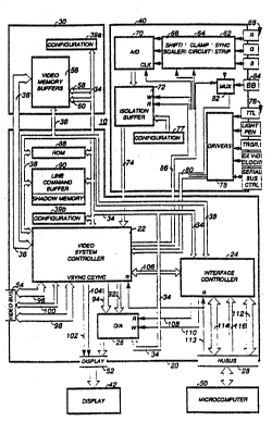
~IG. 1 is a generalized block diagram illustrating a
specific embodiment of a digital video image processing
system 10 according to the invention. The system 10
comprises a video system module 20 coupled as shown to a
memory module 30 and an input module 40 as well as to a
display device 42 and a host control device 50 such as a
procesaor, controller, or microcomputer. In the
illustrated embodiment, the video system module 20
comprises a central motherboard on which the optional
daughter board memory module 30 may be mounted and in
which an optional daughter board input module 40 may be
mounted. Alternatively, other configurations may be used,
for ex~mple, the video processor 20, memory module 30,
and input module 40 may comprise a singie circuit board.
In the il?ustrated embodiment, the video 3ystem module 20
is configured to fit into a conventional NuBus alot of a
host microcomputer via a NuBus connector 28. The host
microcomputer 50 may, for example, be a Macintosh II
computer marketed by Apple Computer Company as in the
illustrated embodiment. Other computers and bus
configurations may also be utilized. In addition, other
controller circuits, such as a microprocesaor or
microcontroller, may be used as the host control
device 50. The video procesqor 20 of the illustrated
embodiment is also coupled to a display device 42 via a
display connector 52 wherein the display device 42 may be
any video display device usins any video standard
including, for example a monochrome or color CRT monitor,
an LCD display, an electroluminescent display, etc. The
video system module 20 may also be coupled to external
.
: . , .: .': .' ' , ~- : - : '
-. : . . . : . . .
. . -. ~ . , :
WO 91/08638 PCI'/US90/06431
video devices or systems -cluding another video qystem
module 20 via a video bus cJnnector 54.
The memory module 30 which provides digital video data
memory for the system comprises primarily video memory
banks 56 made up of dual por~ video dynamic random access
memory (VDRAM) wi~h 0 ~o 8 megabytes of VDRAM (e.g.,
using TC524256 VDRAM chips marketed by Toshiba). The
video memory 56 is normally divided into four eight-bit
deep video banks ABCD ~alpha, red, green and blue (ARGB))
and is used to hold digital video image data. The video
memory banks 56 are coupled to an address/data bus 34 via
. . . .
a multiplexed address bus 58 (10 bits in the illus~rated
embodiment) and a data bus 60 ~32 bi~s in the illustrated
embodiment) as shown. The address bus 58 permits
addressing the video data and the data bus 60 permits
p_ssing da~a to and from the computer S0 via the video
system module 20.
A qerial video data bus 36 is coupled from the video
memory banks 56 to a programmable video system
controller 22 of the video system module 20, as shown.
~he video system controller 22, currently consisting of
two cloqely coupled custom chips but could be contained
in a single custom chip, -ontrols most of the video
special effects processing capability of the system 10
and controls the read/write video memory banks 56 on the
video data bus 36. In the illustrated embodiment, the
qerial video data bus 36 is a bi-directional 64 bit bus
(two-to-one interleaved 32 bi~ bus) which provides video
both to and from the ?0 banks 56 which are
r nized with a t pixel int vec configuration. R
;i rol bus 38 (48 nes i -n 1;~- ~ted embodiment)
provides control s nals to ne vide Inks 56 from the
..
.
.; . ~ ' . .
W O 91/08638 ~ t~ PCT/US90/06431
video system module 20 including row addreqs -~elect,
column address select, write enable, read enable, serial
clock, and serial enable. A configuration register 39a is
coupled to the address/data bus 34 to provide memory
configuration information (i.e., amount of memory
installed) to the system module 20.
The input module 40 provides for optional input signals
including analog to digital capture of analog video at a
programmable sampling rate. The input module 40 may
accept mul~iple (three in the illustrated embodiment)
analog video inpu~s (69) wh-ch are coupled to an analog
inpus circuit composed cc a syn- strip circuit 62, a
clamp circuit 64 and a shift/scaler circuit 66, as shown.
The three inputs, for example, may be three color
compGnents Red (R), Green (G), or Blue (B); a luminance
component and two chrominance components; or, any other
three components of a conventional video format. Four
inputs may be uqed to provide, for example, for input of
four components A R G B. The three analog signals are
coupled from the shift/scaler circuit 66 to an analog to
digital (A/D) converter 70 (e.g., made up of three model
CXA1096 converters marketed by Sony) which sample the
three analog signals and converts each to digital form
(e.g., 9 bits each).
The resulting 24-bit digital data is then coupled from
: the converter 70 through an isolation buffer 72 to the
video system controller 22 of the video system module 20
via a 24 bit data bus 74, as shown. A configuration
register 76 is coupled to the bus 74 via the buffer 72 to
provide iden~ification configuration information (e.s.,
; sample rate, analog video format) to the video systemmodule 20 during power up. The configuration register 77
i .- .. . .
- ' . ': ' - '
WO 91/08638 PCl-/US90/06431
2r~
in the illustrated embodiment comprises a set of
resistors which are r~ad duri~g power up by disabling the
isolation buffer output and reading the bus lines coupled
to the register 77.
The input module 40 also provides for a set of external
inputs 76 including a ligh; pen input, an external
trigger input (e.g., light pen trigger), a TTT video sync
input, an external video clock input (e.g., for genlock)
and a bi-directional serial control/data bus ~e.g., to
interface to conventional video integrated circuits), as
shown. These signals are coupled through driver buffer
ci:cuitry 78 to the video system controlle_ 22 via a
control signal bus 80. A multiplexer 82 couples a sync
signal stripped from the incoming video signal by the
sync strip circuit 62 or a black burst sync signal from
an input 84 through the control bus 80 to the video
system controller 22 under control of a select signal
coupled from the video system controller 22 via a control
signal bus 86, as shown. The bus 86 also couples control
signals from the video system controller 22 to the
shift/scaler circuit 66 ~i.e., a reference level signal)
and clamp circuit 64 (i.e., a clamp window signal) as
well as sample clock and reset signals to the
converter 70 and isolation bu.ffer 72.
In operation, the sync striF circu_t 62 strips off the
aynchronization signals from the input analog video
signals and couples a stripped sync signal to the
multiplexer 82. The stripped analog signals are coupled
to the clamp circuit 6~ ,hich detects the DC level of the
video during a time w: aw supplied by the video system
controller 22 via the _ontrcl bus 86. The shift/scaler
circuit 66 then level shifts o- scales the input analog
.
; ~ ' ' .' ' ~ :'
, ' : ; ~ ' - , . ''
: ' ' ' . . .
WO 91/0~638 1 1 PCI'/US90/06431
signals to put the analog signals into the proper.range
for the A/D converter 70. The analog ~ignals are coupled
to the A/D converter 70 and the sample clock signal from
the video system controller 22 controls sampling of the
analog signal by the A/D converter 70. The resulting
digital output from the A/D converter 70 is coupled to
the video system controller 22 through the isolation
buffer 72 to the video system controller via the data
bus 74. The multiplexer 82 couples either the black burst
sync signal or the stripped sync signal to the video
system controller 22 under conrrol of the controller 22.
... . . . . .
The controller 22 may then use the selected sync signal
or the TTL sync signal in conjunction with the digitized
video data.
In addition to the video system controller 22, the video
system module 20 includes an interface controller 24, a
triple D/A converter 26, a declaration read only memory
(ROM) 88, and a line command and shadow memory buffer 90.
The ROM 88 and buffer 90 are coupled via the control
bus 38 and the data/address bus 34 to the video system
controller 22, the interface controller 24 and the D/A
converter 26, as shown. In the illustrated embodiment,
the declaration ROM 88 is a 256 Kbit, electrically
erasable programmable ROM (e,g,., X28C256 EEPROM marketed
by XICOR~ to which are coupled- chip select, read enable
and write enable control signals from the control bus 38
as well as twenty SiY. address and data lines from the
address/data bus 34, ~he line command buffer and shadow
memory buffer ~shadow random access memory or SRAM) 90
comprices 128 Kbytes of random access memory (e.g., TC524
256 marketed by Toshiba) to which are coupled clock row
and column address select, read enable and write enable
: `
. ' .
W O 91~08638 PCT/US90/06431
'~a?~ 12
control signals from the control ~s 38, aa well as
twelve addreas and data lines from the addreaa/data
bus 34.
The declaration ROM 88 in the illustrated embodiment
containa conventional data that is needed on any circuit
board which is to be installed in a Macintosh Nu~us bus
baYed on the published NuBus protocol. This data contains
information setting video modes, colors and a number of
other parameters. The declaraticn ROM 88 is configured to
allow the host ~acintosh II computer to read the data at
system power up via the interface controller 24. In
.. . . ...
addition, the EEPRO~ o- the _llustrated embodimen.
permits the data to be erased and reprogrammed under
software control. The video system controller 22 in the
illuatrated embodiment also includes a configuration
register 39 which is coupled to the address/data ~Is 34
to provide syatem configuration information to the system
module 20. In the illuatrated embodiment the
configuration regiaters 39 and 39b compri3e resistors
connecte~. at one end to ground or to the supply voltage
and coupled to lines of the bus 34 which are read by the
video system controller 20 during power up.
The line command and shadow memory buffers 90 may be
loaded with information from the host microcomputer 50.
The line command buffer stores commands for line by line
control of video. Thus, line commands are uaed to
override various of the current settings affecting
operation of the video display on a line of video, after
which the settings revert back to the original values.
The line command buffe- comp:iaes 126 Kbytes in the
illustrated embodiment and is organized s that the
first 16 commands correspond to the first c_splay line,
W0 91/08638 ;~ ~r~) PCI /US90/06431
the next 16 commands correspond to the aecond diqplay
line, etc. The shadow memory comprises 2 ~bytes of random
access memory which is used to store the status of system
internal latches and registers which are not readable to
provide bacX-up which permits the system to read the last
setting of the register.
The video system controller 22 is coupled to the video
memory buffers 36 via the video data bus 36, the control
bus 38 and the address/data bus 34, as shown. The
controller 22 is also coupled to the input module 40 via
the control buses 80, 66 and the data bus 74, and to the
D/A converte- 26 via a control bus 9~ and a video data
bus 94, as shown. A bi-directional video bus port 54
permits add_tional digital video sources to be coupled to
the controller 22 including another video system
module 20. The bi-directional video bus port S9 couples
digital video data to and from the video .~ystem
controller 22 via two bi-directional digital video data
buses 96, 9~ (e.g, 32 bit buses allowing four B-bit video
components in the illustrated embodiment) and a bi-
directional control bus 100 providing cloc~, horizontal
sync, and ver~ical sync signals. The video system
controller 22 also couples a vertical sync signal
line 102 and a composite sync signal line 104 to a
display output port 52, as shown. The video system
controller 22 performs prog,rammable real-time video
processin~ of the various video sources from the memory
module 30, input module 40, the interface controller 24
and a video bus por; 54 under control of the host
compute_ 50 via the interface controller 24 to produce a
wide variety of video eff?c~c.
' ~ :
. , .
WO 91/08638 PCl'/US90/06431
14
The interface controller 24 which primarily controls the
interface between the module 20 and the host computer 50
is coupled to the video system controller 22 via a
control bus 106. In addition, the interface controller is
coupled to the controller 22, the video memory
buffers 56, the ROM 88, and the line command and shadow
RAM buffers 90 via the address/data bus 34. The D/A
converter 26 is coupled to the interface controller 24
via the address/data bus 34 as well as the read line 108
and write line 110. The interface controller 24
inter~aces to the hos: computer 50 through a bus
. _ ... . . . .
connector port 28, which is a NuBus connecto_ in the
illustrated embodiment. The Nu8us connector permits the
video syqtem module 20 to fit directly into a NuBus slot
of a host Apple Corp. Macintosh computer and thereby
perm.its transfer of data to and from the host
computer 50. The NuBus connector 2B is coupled to the
interface controller in accordance with the NuBus
standard via a multiplexed bi-directional address/data
bus 112 (e.g., 32 bits in the illustrated embodiment), a
bi-directional control bus 114 (e.g., 12 bits in the
illustrated embodiment) and an ID bus 116 ~e.g, four bits
in the illustrated embodiment). A reset line 113 is also
coupled from the NuDu connector to the interface
controller 24 and the video-system controller 22, as
shown.
The D/A converter 26 (e.g., a Bt473 RAMDAC marketed by
~rooktree Corp.) converts digital video signals coupled
~rom the vid~^ system controller 22 via the video data
bus 94. The resulting analog sigr s are coupled to t
display connector 52 and thr; ~h ~o the displ
device 42. The D/A converter 2- in the :lustrate
: ~ - : .
:: . .:. -: -
: . ,
WO 91/08638 PCr/US90/06431
'~1?~
embodiment is a 24-bit tripie D/A converter which
converts three digital video components to three output
analog video components (e.g., R,G,B,). Control signals,
including sync, blan~ and clock signals are coupled to
the converter 26 via a control bus 92, as shown.
Synchronization signals for the video display are also
provided by the sync signal lines 102, 104. The Brooktree
RAMDAC converter 26 also permits gamma correction to
permit compensating for the non-linea_ signal response of
many display devices usins look-up tables in the
converter 26. Three eables ~i.e., registers) are loaded
.. . ... . .. .. . .
and controlled by the host computer 50 through the
interface controller 24 via the address/data bus 34
(e.g., the eleven least significant bits of the bus
providing 8 bits of data and 3 hits of address) and
read/write lines 108, 110.
Referring now to FIG. 2, there is shown a detailed block
diagram of a specific embodiment of the interface
controller 24 which receives addresses, data and control
signals from the host computer 50 on the address/data
bus 112, control bus 114 and ID bus 116. This information
is used to generate and pass addresses, data and control
signals to load the video memory banks 56, and the
various buffers and registers of the programmable video
system controller 24 and D/~ converter 26 via the
address/data bus 34, control bus 38 and control bus 106.
In addition, the interface controller provides address,
data and control signals to the host computer 50 via the
buses 112, 114. Thus, the in~erface controller primarily
controls communications between the host computer S0
(e.g, through the NuBus in the illustrated embodiment)
and the video system module 20. The interface controller
WO 91/08638 PCr/US90/06431
16
also implements the loading and reading of the ~hadow
RAM 90 to permit reading of register status, implements
an address offset capability, performs a timing register
protection function, and generates a programmable refresh
signal for refreshing the dynamic RAM of the video memory
banks 56.
Address and data information is coupled between the host
computers 50 and an address/data processing circuit 118
on the bi-directional address/data bus 112 through the
NuBus connector 28. In addition, control signals on the
bus 114 and ID signals on the bus 116 are coupled between
the hos; compute: 50 and a NuBus control circuit 120
along with a reset signal on the reset line 113, as
shown. The processing circuit 118 comprises a data
router 122, an addre~s processor 124, and a timing
register protection circuit 129. In addition, a set of X
and Y address offset registers 126 is coupled to the
address proceasing circui~ 118. The register addresses
are shown in abbreviated for with x signifying an offset
from a base register addreqs (which SFsF00000 in the
illustrated embodiment). This convention will be used
hereinafter. All registers within the interface
controller 24 are loaded by the address/data processor
circuit 118 via a bus 131, as shown. Addresses and data
are coupled to and from the data router 122 of the
processing circuit 118 to and from the other buffers and
registers of the video system module 20 and memory
module 30 via the address/data bus 34. In addition, the
addres~es and data are coupled between the processing
circuit 118 :d a system memory controller 128 via an
~ddress/data bus 130. Decoded operation signals are
coupled from the processing circui. 118 to the system
:
' , ~ : ~
. : :
wo sl/ns63s PCr~l 'S90/06431
17
memory controller 128 via a bus 13' and a security
inhibit signal is coupled to the system memory
controller 128 on a control line 134, as shown.
; A valid addrecs signal is coupled to the NuBus control
circuit 120 on a control line 136 and a store enable
signal is coupled rrom the Nu3us control circuit 120 to
the processing circuit 118 on an enable line 138, as
shown. The NuBus controller 120 also generates a
read/write enable sisnal which is coupled to the system
memory controller 128 by an enable line 140 and generates
a data available signal to enable a data read or write
... . .. . .
cycle which is coupled to the controller 128 by a control
line 142. In addition, the system memory controller 128
generate~ an acknowledge signal in respon~e to completion
of a data read or write cycle which is coupled to the
NuBus controller 120 on a control line 144. The control
bus 106 which connects to the video system controller 22
couples an interrupt signal to the Nu8us controller 120
on an interrupt line 146 and couples a video RAM transfer
request signal to the refresh generator 156 on a control
line 148, as shown. In addition, the Rystem memory
controller generates a video memory data transfer enable
signal and register data enable signal which are coupled
to the control bus 106 on enable lines 150 and 152, as
shown.
The interface controller 24 primarily synchronizes
address and data exchange with the NuBus and controls
transfer to and from the video memory 56 and various
system registers. ~hus, the host computer transfers data
by generating an identification code (ID) on the ID
bus 116 which identifies to the board its slot in the
':
bus. At the same time, an address is applied by the host
;
:
,~ . , .
.
.
WO 91/08638 l 8 PCr/US90/06431
compute- on the addreqs/data bus 112 followed by data
~i.e., bus 112 is time multiplexed between address and
data~ which is processed by the addreq~ procesqor 124 to
determine if it iS a valid board address. If it is a
valid address, a signal is ~nt to the NuBus
controller 120 on the control line 136 which is used by
the NuBus controller in conjunction with the proper ID
and the NuBus control signals from the control bus 114 to
generate and send a store enable signal to the
address/data processor 118 on the enable line 138. In
response to the enable signa`, th~ processor 118 stores
.. .. . . .
the incomin~ address and on tne ne~: clock cycle stores
the associated data in in~ernal registers with the proper
timing as dictated by the NuBus protocol. ~hus, the
addreqs~data bus 112 is de-multiplexed by the
address/data proceqsing circuit 118. The data router 122,
comprising primarily a set of gates and
multiplexer/demultiplexers, rearranges the address and
data and couples tr 1 to the proper bus 34, 130 to
tranqfer the data to the addre~sed video memory bank or
system register. The address may al~o be offset by a
predetermined number in either the x or y axis by the
data router i22 based upon values stored in the x and y
offset registers 126.
~hus, the data router 122 arranges addresses and data to
be put on the bus 34 to be stored in the video memory
banks 56, or for loading internal registers in the video
system module 20. Conversely, the processing circuit 11~
may couple data back to the host microcomputer 50 with
the data router 122 arranginc ~he data in proper format
and multiple~ing it on ~o the bus 112 with the NuBus
.
. , : . .
,., :
~- , :
WO 91/08638 PCl`/US90/06431
19
;S ~
controller generating the proper control signals in
accordance with the Nu~us pro~ocol.
To accept data from the host microcomputer Nu~us
interface, the processing circuit 118 can utilize a
pipelining technique in which the data and address are
stored after which another cycle o' reading and saving
data and address information is initiated by an enable
signal on enable line 13a at the same time that the
previously stored data ~s transferred to system memory.
To control the transfer Oc data to system memory, the
address processor 124 decodes the address and proviaes a
control signal on the control bus 132 to the system
memory controller 128 to identify the addressed segment
of system memory (i.e., video memory, EEPROM, system
registers, etc.). The NuBus controller 120 generates a
data available signal which is coupled on line 140 to the
system memory controller 128 to indicate that data and
address information is stored and ready to be
transferred. In response, the system memory
controller 128 generates control signals to control
transfer to or from the appropriate system memory
location. After the transfer, the ayAtem memory
controller 128 sends an acknowledge signal to the NuBus
controller 120 on control line 144. The system memory
controller 128 also generates control signals on the
bus 130 to control the multiplexing of the data/address
information by the data router 122. Thus, the system
memory controller generates the control signals which
control the transfe_ of data to and from the system
memory. This process is controlled by data stored in
system memory controller register 154 which are loaded
with data via the bus 130. The system memory
WO 91/08638 PCI/I'S90/06431
controller 128 also compriqes a progranunable r,efresh
generator which generates a aiqnal to activate a refreqh
cycle c the dynamic ~A.M inqtalled in the syqtem at an
interval which is prog:ammable by loading the desired
value in the associated one of regi~ters 154.
The transfer of da~a to registers which control timing of
horizontal and vertical control signals is protected by a
key code security system 129 incorporated in the address
processor 124. If a protected timing register is
addre~sed, the protection circu t 129 inhibits the system
memory controller 128 unless a key register 133 couplec
to the protec~ion cir_uit 125 has been loaded with the
proper key code on the previous data load cycle. The
protection circuit 129 generates an inhibit signal which
is coupled to the system memory control r 128 on the
control line 134 and which inhibits the c~ trollçr 128.
If the key register 133 is first addresqed and loaded
with the proper code, the inhibi signal is not generated
and the system memory controller 128 can generate the
necessary control signals and transfer the data. This
protection circuit 129 thus protects against accidental
overdriving of the horizontal or vertical circuits of the
display device 42.
FIG. 3 is a detailed block diagram of a specific
embodiment of the programmable video syqtem
controller 22. The video system controller 22 provides
the primary capability for video data manipulation and
processing of video data from multiple input sources of
video data for the system 10. The controller 22 is
programmed by the host computer 50 by loading internal
regi~ters of the controlle; 22 through the inter4ace
controller 24 via the address/data bus 34. Thus, the
.
.
. : .
" :
WO 91/08638 PCI/I IS90/06431
21
2~?` ' ~
address of the register to be loaded and the data to be
loaded into the addressed register are coupled on the
address/data bus 34 to a register interface 160 of the
controller 22. The regi~ter interface 160 couples the
incoming address and data information and control signals
to a bus 162 which couples address data and control
signals to all the internal registers associated with the
functional blocks of the video system controller 22. The
interface registe- 160 thus controls the loading of the
registers internal to the controller 22. The control
signals for loading the register are generated utilizing
timing signals couDled to the reg~ster interface 160 from
a relative timing circuit 164 and an absolute timing
circuit 166 via timing signal bus 168, as shown. Contro~
signals are also coupled between the register
interface 160 and the interface controller 24 via the
control bus 106. A reset signal is coupled to the
register interface 160 on the reset line 113. The
regi~ter interface 160 also controls coupling of signals
and data back to the host computer 50 through the
interface controller 24 via the bus 34.
The absolute timing circuit 166 generates programmable
synchronization signals optionally locked to an external
synchronization or video source, including horizontal and
vertical blanking, and front and back porches. ~hus, the
absolute timing block can provide a wide variety of
programmed or genlocked synchronization and timing
signals to generate or syrlchronize with almost any video
standard. These synchronization signals are coupled to
the various function circuits o' the controller 22 via a
sync bus 170, the csync line 104, the vsync line 102 and
the control bus 92. In addition, the absolute timing
WO 91/08638 PCI-/US90/06431
22
circuit 166 generates timing sicn :s tc control capture
of video data to the video memor which are coupled to
a video capture multiplexe~ 190 ~ a ccntrol bus 172 and
to the input module 40 via the control ~us 86, as shown.
Programmable llne, field, and frame interrupts, as well
as light pen interrupts, are also generated by the
absolute timing circuit 166. The absolute timing circuit
utilizes system and pixel clock signals coupled from a
master clock generator 184 on a clock bus 186, external
signals coupled on the buses 80,100, and capture window
enable signals coupled on an enable bus 174 to generate
; synchronization, capture enable and interrupt signals.
The absolute timing circuit 166 also generates timing
signals which are coupled to the relative timing
circuit 164 via a b~s 165, and absolute x and y pixel
coordinate signals which are coup~ed to a window control
circuit 176, a line control buffer 118 a multiplier 202
and a color look-up table 180 via a bus 182, as shown.
~he relative timing circuit 164 is a programmable circuit
which controls relative video memory bank configuration
to control concatenation of the video memory bank via a
control bus 38 to permit the video memory banks to be
configured in many arrangements. It also generates
control signals to coordinate use of the video bank for
capture of video data and couples control signals to the
video capture multiplexer 190 via a control bus 188, as
shown. The relative timing circuit 164 also processes
absolute timing signals coupled from the absolute timing
circuit 166 on a line 165 and generates video memcry bank
addressing to allow for special efects such as panning,
zooming, mosaicing, etc. An address translator within the
relative timing circ : 164 permits remapping of the
. .: . :
.: ' , : : ' '
.
WO 91/08638 PCl'/US90/06431
23
Z~
addre~ses provided by the absolute timing ~ection to new
addresses. Control signals are also generated to control
a video input circuit 192 to control video input from
several sources. The relative timlng circuit 164 utilizes
timing signals coupled f rom the absolute timing
circuit 166, and enable signals from the window control
circuit 176, as shown, as well as clock signals coupled
from the clock generator 184 via the clock bus 186.
The video input circuit 192 comprises memory decoder and
de-multiplexer circuits which process video data coupled
from the video memory banks 56 via the video data bus 36,
and from the A/D conve_ter 70 of the input module 30
coupled via the data bus 74. Video data may also be
coupled to the video input circuit 192 via the digital
video data bu es 96, 98 from the video port 54. The data
from these sources is coupled by the video input
circuit 192 to one of several internal video buses
including live A/D bus tLADC) 194 (e.g., 24 bits) a live
digital video port (LDIG) bus 196 (e.g. 32 bits), a video
bus one (DV1) 198 ~e.g., 24 bits) and a video bus two
~DV2) 200 ~e.g., 32 bits), which lare coupled to a
multiplier circui: 20., a video ranye thresholding
circuit 204, the color look up tables 180, a display
multiplexer 206 and the video capture multiplexer l90, as
shown. The video input circuit 192 also performs parallel
to serial conversions of video data for di~play of
single, double and quad bit data, as well as parallel
expansion of word data. A decoding function provides the
capability for interpreting and decoding compressed image
formats. Control signals for controlling the video data
input and output are coupled from the relative timing
circuit 164 via a control bus i73, as shown. In addition,
WO 91/08638 PCI'/US90/06431
24
the video input circui~ 192 couples alpha buffer ~d,ata to
an alpha buffer con~rol circuit 212 via a data bua 214
and control aignals to the color look up table 180 via a
control line 216.
The alpha buffer control circuit 212 interprets pixel
values from the alpha buffer of the video memory 56
(i.e., the first of the four video banks) as commands in
sevaral different programmable modes. The alpha pixel
commands enable or disable other opera~ions or modes on a
pixel by pixel basis enabling pixel by pixel control of
the video display. The alpha buffer control circuit 212
utilizes alpha buffer data coupled f-om the video input
circuit 192 via the data bus 214 to generate alpha buffer
control data coupled on a control bus 221 to the
multiplier 202 and a control bus 296 to other func~ional
circuits of the controller 22 to control functions on a ,~
pixel by pixel basis. The alpha buffer control
circuit 212 al~o generates alpha buffer priority data
coupled to the video priority resolver 208 via a control , '
bus 220 and control signals which are coupled to a
thresholder via a control bus 298.
The line buffer control circui_ 178 interprets commands
stored in the line command buffer 90 which are coupled to
the line buffer control circui,t 178 v.a the addreas/data
line 34. Absolute x pixel coordinates are alao coupled to
the line buffer control circuit 178 from the absolute
timing circuit 166 by bus 182, as shown. The line buffer
control circuit reads ca~nmands from the line command
buffer to enable or di: le other modes or operations
before scan lines are r.~ad from video ~- ~ry and at
programmable a_solute x coordina~es along . line. Thus
line baa~s which are coupled to the video priority
,: - :~.
- '.:-:.~ . ::
.- :: . .: : :
W ~ 91/08638 PCTIl~590/0643l
7~ .
resolver 208 via a control bus .22, and generate control
signals on a line basis which are coupled to the
multiplier 202 via a bus 224. In addition, control
signals are generated which are coupled via a control
bus 227 to various functional circuits of the video
system controller 22 to enable or disable functions on a
line by line basis.
The window control circuit 176 generates control signals
to maintain four rectangular window regions in absolute x
and y pixel coordinate space utilizing values loaded into
internal registers. The x and y pixel coordinates are
coupled from the absolute timing circuit 166 via the bus
182. The window control circuit generates window capture
signals which are coupled to the timing circuits 164, 166 `
on the enable bus 174, and generates priority signals
based on internal register values for each of the four
windows to define window boundaries which are coupled to
the video priority resolver 208 on four window priority
bu~es 225, 231, 228, 229. The window priority is
arbitrated within the window control circuit; only the
highest window priority signal is passed to the priolrity
resolver.
The multiplier circuit 202 comprises primarily a matrix
of nine dedicated signed 10 x 9 bit hi~h speed
multipliers which can perform-a multiplication in le~s
time than required to di~play one pixel. The
multiplier 202 can select from six input video sources
which include the live A/D video bus 194, the live
digital video port bus 196, the video bus one 198 and the
video bus two 200, a color look-up table one (CLUTl)
video bus 230 and a colo_ look-up table two (CLUT2) video
bus 232. The multipliers typically multiply a video
- : .
WO 91/08~38 PCI-/US90/06431
26
2~
source by a blending or mixing constant. The multiplier
circuit can perform a matrix transformation on data from
one of the video sources, perform a programmable blend of
up to three of the video sources, perform frame averaging
of an incoming static video signal and execute spatial
filtering on one of the video data sources. The
multiplier utilizes control and data signals from the
alpha and line buffer control circuits 220, 178, as well
as the video sources. The resultant multiplied sisnal is
coupled to a multiplier video bus 234 which couples the
resultant signal to the video range thresholdins
circuit 204, the colo_ look-up table lB0, the display
multiplexer 206 and the video capture multiplexer 190. In
addition, a partial sum is also generated and coupled to
a partial sum bus 236 which is coupled to the display
multiplexer 206 and the video capture multiplexer 190, as
shown. More than nine multipliers may optionally be used,
for example, a four by four array of multipliers would be
used to permit four sources with four components each to
be multiplied by up to sixteen constant values.
The range thresholding circuit 2G4 compares three aets of
upper and lower programmable reference values loaded into
internal registers on a pixel by pixel basis to incoming
video source data on the buses 194, 196, 198, 200, 230,
232, 234. -More than three sets of reference valueq and
comparisons may optionally be provided. Based upon the
comparison, priority and source signals are generated and
coupled to the video prioxity resolver 208 on a priori
bus 240. The range thresholder may also output a priority
and source for those pixels that d--ine a transition or
change in the input video source, such that comparisons
that result in a change of the thresholder output also
,
W O 9l~08638 PCT/US90/06431
27 2~
result in the generation of a programmable plurality of
transition pixel priorities and sources.
The priority re~olver 208 examines six priority input
signals coupled from the alpha buffer control 212, the
line buffer control 178, the range thresholder 204, the
video input circuit 192, the window control 176, and the
color look-up table 180 of the video system
controller 22, each of which has an a~sociated
dynamically programmable priority level and video data
source designation, and determines for each pixel which
video source has the highes~ priority. The priority
resolver outputs an index signal referencing the highest
priority video source on a bus 238 which is used by the
display mu'tiplexer 206 to output the highest priority
video source.
Since the diqplay priority level is programmable, it is
possible that two or more video sources could have the
same priority level for the same pixel. If this priority
level is the highest level at the pixel, ehen an implicit
priority order is used wherein the video data source with
the highest implicit priority is ~elected (e.g., in the
illustrated embodiment the implicit order i3 the order of
the inputs to the resolver 2G8 as follows: bu-qes 220,
222, 225, 231, 228, 229, 201, 203, 181, 183, 240). It is
also possible that there may-be no contenders of any
priority level at a given pixel. In this case, a
programmable default video data source is selected to be
displayed in the absence of any other. The thresholder
circuit 204 also generates control signals which are
coupled to the capture multiplexer via a bus 406, as
shown.
`.:
':
" ;'
W O 9l/08638 PCT/US90/06431
2~
3~)
The display multiplexer 206 selects for display a video
source 'rom one of the video buses 194, 196, 198, 200,
230, 23_, 234, 236 coupled to it unc r the control of the
select signals from the priority resolver 208 on the
select bus 238 and on a default line 239. The selected
video source is coupled to the D/A converter 26 via the
video data bus 94 for display and to the video capture
multiplexer 190 on the data bus 207, as shown.
The video capture multiplexer 190 is a multiplexer and
encoder circuit which controls storing of video data
arriving at its inpu_s into the video memory buffers 56
or coupling the dat_ to the diqi~al vidëo port 54, and
which encodes the video data in~o formats suitable for
writing to the video memory 56 or the digital video
port 54. The input video sources are the video buses 194,
196, 200, 234, 236 and the output data bus 207 of the
display multiplexer 206, as shown. Control and timing
signals are provided from the absolute timing circuit 166
and the relative timing circuit 164 via the control
buaes 172, 188. The video capture multiplexer 190 also
provides aerial to parallel conversion of the video data
for storage of single, or double byte pixel data. In
addition, the video capture multiplexer 190 provides the
capability to encode video data in one of two compressed
forms: YCc and RGB555 and to store a single component of
the video data in any one or all four of the video memory
banks 56. The data is output onto the video data bus 36
to the video memory banks 56 or on one of the digital
video data buses 96, 98, to the dig tal video port 54.
The color look-up table (CLUT) lB0 lS provi~ed to permit
rema?pin~ of colo: Dixel values, CCC decoding, gamma
correction and to ~ vide a hardware cursor mode. The
:. : ~ ,;
, . . . .
,~
., ~ . . .
WO 91/08638 PCl-/l~'S90/06431
29
.
absolute x,y pixel coordinates on the bus 182, C~C bi:
map signals on the bus 216 and video bus sources 194,
200, 234 are u~ilized by the CLUT 180. Baaed on three
inputs the CLUT 180 provides output video da~a to a color
look-up table one (CLUT1) video bus 230, a color look up
table two (CL~T2) video bus 232, and two color look-up
table display priority signals coupled to the ~ideo
priority resolver 208 on the priority buses 181, 183, as
shown.
A color look-up mode permi~s selection of an output pixe'
color based on an index value using three color look up
tables (one for each of three components). An input value
from one of the input video sources is uaed as an index
into all three tables simultaneously. The three values
referenced by the index are then used as color components
of a pixel which are output on one of the video
buaes 230, 232. The color look-up table is divided into
two somewhat similar halves, but both halves can be
joi.ned to provide a color look-up table which is larger.
gamma correction mode permits compenaation for non-
linear charac~eristics of video sources at different
signal levels. In the gamma correction mode, one half of
the table is used as three independent color tables and
each of the three color components of the input video
aource are uaed as an index into it~ own color table. The
values referenced by the indices are then used as the new
color components for the output of the color look-up
table 180. Thus, a video source can have its color
components individually corrected or remapped. In the
hardware cursor mode, the color look-up tables are used
to control a small rec~angular region of pixels at a
programmable continually variable location.
: -
; - .
: - :
WO 91/08~38 PCI-/US90/06431
~z~
The system module 20 s a programmable and highly
flexible digital processin~ device capable of a wide
variety of digital special video effects and video
manioulation. The system module 20, in the preferred
embodiment, plugs directly into a NuBus slot in, for
example, an Apple Macintosh II series computer. The
system module 20 supports all standard video display
modes permitting it to be configured with virtually any
video monitor. The input module 40 supports capture of an
image from an external source which may be such sources
as an RGB video camera, a time-base cor~ected video tape
o- disc player, or virtually any device tha~ can generate
a component RGB video signal. The input module 40 also
supports a light pen and the system module 20 can retain
the last absolute x,y position of the light pen on the
displayed image. Most of the operations of the system 10
are accomplished in the digital domain, and therefore,
there is no loss of detail as commonly experienced with
analog effects. In addition, the effects a e accomplished
in real time in most cases and u;ilize static images,
animated computer graphics, or real-time video sources.
Due to the programmable timing circuitry 18~, 164, 166 of
the video system controller 22, the system module 20
provides highly flexible timing which can be configured
to match the timing specifications of virtually any video
standard such as NTSC, PAL, etc. Timing options include
interlace, repeat field, and noninterlace video
generation. When generatinc an interlace video signal,
the system module 20 can provide equalization and
serration pulaes. r~ata encoded in the vertical blanking
intervals such as SMDTE, V~R, o- closed caption may
normally be blocked but may be optionally passed through.
: ,
.
' : , ' -: :, .
WO 91/0863~ PCI/US90/06431
31
2~
Timing circuity may also be configured to synchronize to
an external video source(genlock) o- an external
synchronization source. The signal generated is in
synchronization with the incoming video signal or ~ynch.
If the incoming video signal or synch timing is of
broadcast standard, the system will produce an output
broadcast standard.
Video data can also be output in analog form using a
conventional D/A converter 26 to encode the signal into
com?osite analog form. A digital video bus port 54 is
provided which permits the exchange of digital video
, .. . .
information w-th othe- digital video devices coupled to
the system. For example, the digital video bus allows
direct interconnection of multiple ~ystem module 20
. circuits or other input or output devices. A wide variety
of digital special effects are made po-~sible by the
programmable multiplier array 202 and other circuits
including mosaicing, pixelization, posterization,
solarization, blending, filtering and anti-aliasing.
These visual effects are generated in the digital domain
and thus many are virtually impo-~sible to do in analog
circuitry.
The mosaic effect replaces an image with feh~er, but
larger "pseudo pixels". This effect may be accomplished
in the horizontal or vertical direction. The ratio of the
~ize of the original pixel to the pseudo pixels is highly
controllable and programmable. Pixelization is
accomplished by mosaicir.g in both the horizontal and
vertical directions. The horizontal and vertical mosaic
factors do not need to be iden~ical. This pixelization
effect can be used in conjunction with live video mixing
to produce the effec_ commonly used to obscure witne~s
:
.
'
. . .
, ~ .
WO 91/08638 PCI/US90/06431
32
2~ ~ J ~ ~
identities c; to censor images for television diqplay.
Posterization is an effect which restricts the image to a
subset of the colors actually present, and qets areas
closely related in color or ~alue to the same pixel color
and value. This effect is similar to the photographic
posterization~effect except that the video effect is
continuously variable and reversible. This effect may be
accomplished by mathematically clipping off less
significant bits of the pixels (i.e., truncation~.
Solarization is an effec~ that creates a false color or
pseudo color effect which is also highly programmable and
reversible.
The system module 20 also provides noise gene-ation which
produces linear and Gaussian white noise to create a
display effect which is similar to that created by a
televi~ion set which is not tuned to a station. Noise
generation is particularly useful for filtering and can
be uYed to control other effects. Since the digital
system module 20 provides sharp transitions in an image,
some aliasing or image artifacts may appear as a result
of the sharp transitions in the image in video formats
such as NTSC. This aliasing can be corrected by the real-
time anti-aliasing capability of the 3ystem module 20
w~ ch iY capable of performing such functions as fades
and mixes while also simultaneously performing anti-
aliasing.
Other special effects include traditional video switcher
effects and image manipulations including vertical and
horizontal scaling, zero orde_ effects and vertical
int :val manipulations. The system module 20 can
ind~-andently scale o zoo,~ an image by integer
multiplication fa- ors in both horizontal and vertical
."
,: , ' . ,
:, -., , . :
': , '- ' ' ' ~ ': :: :
.
,
WO 91/08638 PCl'/US90/06431
33
;2 r~
directions. The appropriate part of the image is
replicated along a line in the horizontal direction and
the appropriate video lines are repeated as needed. A
vertical mirroring effect can be produced by the system
module 20 by displaying the top half of the di~play in
reverse vertical order from the bottom half. Any kind of
repeating oz mirrorins in the vertical direction is
possible, including vertical reversals or flips and
venetian blind effects. Rolling or panning can be
performed by displaying different parts of the same image
over time. Horizon~al and vertical rolling can be
, . . , _ . . . . . .
performed independent of each other. ~f an image is being
diqplayed which is much larger than the display area, the
image can be "paged through~ one diqplay screen at a
time.
Conventional video effects such as pulls and puqhes csn
be performed by capturing the video signal and uqing the
appropriate rolling effect. A drop chadow effect can be
produced which edges a video image or portion of an image
with a selected color or effect. The system can also
capture such signals as automated color signals, SMPTE,
time code ~ignals and other codes that are inserted into
the vertical interval in a video signal and can paqs them
through or remove them. Some subsets of these codes such
as the SMPTE code can be generated or modified as well.
The qystem module 20 is also capable of character
generation and can operate in an anti-aliasing character
generation mode in which high quality character
generation is produced with the number of fonts, faces,
styles and sizes limited only by the hos~ computer
software. The system still retains the capability to
- '
-
. ~ '' . . . . .
WO 91/08638 PCI/US90/06431
34
Z~
perform such functions as fades and mixes while in this
anti-aliasing graphics mode.
Other special video effects such as wipes, fades, video
mixing and thresholding are othe- video effects and
functions which may be performed in real time with the
qystem 10. A wipe can be performed from one image source
to another with virtually any direction and speed. A fade
can be accomplished by mixing a percentage of one image
w:~h a percentage of another image. Video mixing allows
tne video to appear to overlay or go behind other video
sources. Multiple windows can also be controlled in real
time. Operations such as geometric dissolves, fades, and
mixes between two image sources are supported and include
square, circular, triangular or other shaped transitions
from one image to the next. Any arbitrary shape or shapes
can be programmed in switching from one video -~ource to
another, and the switc can be hard or qoft edged. These
effects can be controlled on a frame by frame, line by
line, or pixel by pixel basis.
The system module 20 also provic for blending or mixing
~perations by taking a qelectec rcentage of one image
ano ~dding it to a -~elected perc_ntage of another image.
A s~lected percentage of a third image may be blended in
as well. This third image could :: used, for example, to
add a texture to the blend of the first two. This video
mixing is accomplished under the cor.trol of a digital
fader or level control and noise generation can be used
to control blending or mixing c_ the two images.
Th-. ~olding allows a range comparison to be made on a
cor nt of color. The result of this comparison can be
uqeo, ror example, to determine a "key" to control which
video source to display a. any point on the screen.
:
. . .
WO 91/08638 PCI-/US90/06431
. .
Multiple thresholders 204 in the system module 20 can be
logically combined to create key methods that are
currently unavailable, as well as standard types, like
"chroma key" and "luma key". Shadowed areas in a chroma
key area can be used to alter the luminance of the
backsround graphics, creating a live "pseudo shadow" on
top of the graphic image.
Image capture capability is also provided by the input
module 20 which involves a digitization of live video
signals from an ex~ernal analog source and recording the
data into digital video memory 56. System module 20 in
conjunction with the input module 40 is capable of
continuously capturing a complete color video frame in
real time and processing the digitized data in real-time.
For example, a standard NTSC mode frame can be captured
30 times a second with the capture rate flexible enough
to be compatible with the characteristics of virtually
any incoming video signal. Strobing may be accomplished
by repeatedly capturing a video image and holding for
short duration before capturing the next image. Selective
capture is provided by restricting the capture of live
video on a line by line or pixel by pixel basis. The
~ystem provides direct support of RG3 color space and can
be configured to work in YW, YIQ, and other common color
spaces.
~he system module 20 supports many computer display
modec, including the standard display modes of the Apple
Macinto~h II series compute:. Color look-up table
operation modes including the Apple Standards are also
supported wherein the display shows a numbe- of user
selected colors from a palette of over 16 million colors.
In these modes, a reasonable selection of colors is
W O 9~/08638 PCT/US90/06431
36
7 ~
attainable using a amaller amoun~ of memory for the image
itself. The~e modes are commonly called one, two, four
and eight bit color loo~-up table modes. Additionally,
the qyqtem module 20 ~upports a nine bit color look-up
table format. In the one bit color look-up table mode, a
sinqle bit in the image memory determines which of two
colors, each specified with 24 bits RGB precision, is to
be displayed at that pixel. A 2 bit mode utilizes two
bits in the image me-~ry which determine which of four
colors, each specifi~e with 24 bit RGB precision, is to
be displayed at each pixel. ln a 4 bit mode, a group of 4
... .
bits in the image memory determines which of 16 colors,
each specified with 24 RGB precision, is to be di~played ,
at each pixel. An 8 bit mode provides a group of 8 bits
- in the image memory which determine which of 256 colors,
each specified with 24 bit RGB precision, is to be
displayed at each pixel. The 9 bit mode provides a group
of 9 bits in the image memory, which can be u ed in two
different ways: it can determine which of 3B4 colors
each specified with 24 bit precision is to be displayed
at each pixel, or it can determine which of 512 colors,
the first 256 of which are specified with 24 bit
precision and the second 256 of which are specified with
16 bit precision,is to be displayed .. each pixel.
In addition, a di:ect pixel displai mode is provided in
which millions of colors may be displayed simultaneously
with the only limit being the number of pixels on the
screen. The direct pixel display is provided in a 16 bit
mode in which a group of 1 bits are treated in four
parts, 5 bits each for red, en and blue components,
and 1 bit which is design as an alpha bit whose
significance varies. This m .s also known as the RGB
. " ,
. ' : ~ - . .
:: :
: ~
WO 91/08638 PCI-IUS90/06431
37
555 mode. An RGB 5 6i mode in which the green component
uses six ~its (the original five plus the alpha bit) is
also provided. A 32 bit mode is also provided in which a
group of 32 bits are treated as four parts: 8 bits each
for the red, green, and blue components, and the B bits
left over are designated as an alpha byte, whose meaning
is variable. This mode is also designated as the RGB 888
mode. The system 10 Can use the eight bit alpha byte for
a wide variety of enhanced effects which can be performed
on a pixel by pixel basis. Since only 3 sets of B bits
are being used for color information, this mode is also
sometimes referred to as a 24 bit mode. TP Filtering
operations are also provided which allow the color at any
location on the -qcreen to be affected by the colors
around it. Filtering operations can be affected by
selected color space components at each location.
Using the memory module 30, the system 10 in the
illu~trated embodiment Can Contain up to B MegaBytes of
video memory in the form of conventional video DRAM. This
memory is contiguous in the system address ~pace and is
organized such that consecutive raster lines are an equal
distance apart in memory. This distance between lines is
called rowbytes, and is even. Also video memory Can be
used for capturing images using the A/D converter 70 of
the input module 40.
Video memory is divided into four banks - A, B, C, and D.
These banks normally hold images that can be displayed.
When di~playing from video memory, many different modes
are possible. The moSt straight forward mode contributes
the red, green, and blue components from the B, C, and D
banks. Othe. modes may display from just a single bank,
or a concatenation or combination of multiple banks. For
. ' ~ ~ ~'' '' ',
: : . ' - : . .
WO 91/08638 38 PCI/I,'S90/06431
Z~
example, the A and B banks can be treated as independent
8-bit/pixel banks ~e.g. eight bit color look up table),
or can be combined to act as a single 16-bit/pixel bank
(e.g. RGB555)~ Alternatively, ~he banks can be
concatenated horizontally or vertically. For example, two
lXxlK 8-bit banks can be treated as two separate 8-bit
banks, as a l~x2K 8-bit bank, as a 2~xl~ 8-bit ban~ or
as a 1~xlK 16-bit bank. Although the A and B banks ~ere
used in this example, these banks would be used for
displaying red, ~reen, an~ blue component data.
In addition, there is great flexibility in the way the
ban~ data can be displayed. T,~ bank data can represent a
color look up table ~CLUT) image, where each pixel value
represents an index to an RGB color. ~he bank data can be
combined into direct pixels, where each pixel has red,
green, and blue components which directly repre~ent a
color. The banks can also represent YCc (this notation is
short for YUV or YIQ), DYUV, or CCC pixels (which are a
compre~sed form of YCc or RGB pixels).
The position and timing for each bank is independently
controllable relative to the absolute screen position.
Each bank has an a~sociated X and Y offset (this can be
used for panning)~ a horizontal and vertical zoom factor,
and a horizontal and vertical mosaic factor for varying
the position of the bank and apparent pixel size. The
horizontal and vertical zoom and mosaic factors are
independent so that the aspect ratio may be altered. The
video system controller 22 can manipulate a variety of
display ~ources and control their display on a pixel by
pixel basis using display priorities. Th at any given
pixel, the highest p- ority display sourc .s selected by
the priority resolve_ 208. For example, if there are two
`''
'' ' . .
,'
WO 91/08638 PCl-tUS90/06431
39
,- ' 2
rectangular windows which overlap, the window with the
highest display p:iority is displayed as if it is on top.
There are seven different display sources that the video
system controller 22 can control in one of two formats;
twenty-four bits RGB, or eight bits gray scale. When an
eigh~ bit display source is selected, the eight bits are
copied to each of the red, green, and blue components,
thus providing a 29 bit grey scale display source. There
are three fixed format sources which provide 24 bit data
and three fixed format eight bit sources which provide 2~
bit gray scale data. The thirteen different display
sources are - Live Ainr Live Digital In, Video Bus one,
Video Bus two, CLUT 1, CLUT 2, multiplier output, partial
sum output, default color one, default color two, Live
Digital in alpha channel, Video Bus Two alpha channel,
and truncated partial sum output. The first seven of
these display sources are the seven dual format sources.
The nex~ three of these display sources are the three
fixed 24 bit sources. The last three of these display
sources are the three fixed eight bit sources.
Analog live video can'be fed to the input module 40 and
the analog signal may be converted to 24 bits (8 red, 8
green, and 8 blue) by the analog to digital
converters 70. These 24 bits are put on the Live A/D
video bus 194 ~LADC) and can be selected as one of the
RGa display sources. The 32-bit digital video port 54 can
accept live digital 32 bit data (Live Digital In bus 196-
LDIG). This could fo- ~xample be from the output of
another ~ystem module 20. The low 24 bits of this can be
selected as an RGB display source. The upper eight bits
can be used to represent an intensity, and can be
selected as an eigh bit display sou:ce (which is
;:
:
~ - .'. ' , ' ' ', .
WO 91/08638 PCI/US90/06431
: 40
expanded to 24 bits~. The video system controller 22
contains two internal video buses: Video 3us One 198, and
Video Bus Two 200. Video Bus One is a 24-bit RGB data
path and Video Bus Two is a 32 bit ARG3 data path. These
data paths carry digital video information just as the
Live A/D and Live Digital in data paths. However, in this
case, the source of the information on the video buses
comes fro~ the video memory banks 56.
The video system con~roller 22 also contains two Color
Look Vp Tables (CL~) which expand color indexes to 24-
bit RGB data sources 230, 23_. In addition, each CLUT can
be put in a hardware curso- mode which displays a ï6x16,
or 32x32, 24-bit image. ~hese CLUT sources 230, 232 are
two of the RGB display sou-ces. The multiplier 202
outputs can also be used as a display sources. In some
modes, the upper eight bits of the multiplier array
sum 236 may represent a partial sum output and can be
used as a gray scale display source. Two additional video
sources are provided by two default color registers with
each register represe~ ing a 24-bit RGB color. Both
default colors can be u :d as display sources.
Referring now to FIG. 4, there is shown a detailed block
diagram of a specific embodiment of the video input
interface 192 compri~ing primarily a serial data
multiplexer 260 and a video routing multiplexer 262,
together with an input drive. 264 and an input select
circuit 266, as shown. Serial digital video data is
coupled to the aerial data multiplexer from the video
memory 56 via the video data bus 36 made up of four
component buses 268, 270, 272, 27~ for the alpha red,
green and blue componen~s. In addirion, 2 set of control
signa. is coupled to the serial data multiplexer from
'.-
.
-
WO 91/08638 PCI/I-'S90/06431
41
the relative timing circuit 164 via the bu~ 173 and a set
of control registers 280 also provide initial values of
the DY W mode. The serial data multiplexer demultiplexes
the serial data from the bus 36 and couples it through on
a 128 bit video data bus 226 to the video routing
multiplexer 262. The control signal bus 173 includes a
control line for initializing the DYUV mode and a data
bus 228 couples DY W decoded data from the ~erial data
multiplexer 260 to the video routing multiplexer 262. The
control signal bus 1~3 also couples con~rol signals to
the videa routing multiplexer 262, as shown.
Also coupled to the video routing multiplexer 262 is a
set of control registers 281 which are coupled via a
: control signal bus 282 to the video routing
multiplexer 262. The control registers 281 are the
display bank mode control regi~ters which are loaded by
the register interface 160 via the bus 162 ~see FIG. 3)
.' thereby permitting programmable control of the video
. input interface 192. The video routing multiplexer 262
decodes video pixel data and couples the video data to
the video data bus One (VDl) 198 and the video data bus
Two ~VD2) 200 depending on the status of the control
registsrs 281. In addition, the video routing multiplexer
: may generate a display priority and source signal on the
. priority bus 201 and 203 whic~ are coupled to the video
priority resolver 208. The multiplexer 262 also couples
: the alpha buffer data to the alpha buffer control 212 via
the bus 214 and generates a color look-up mode control
signal on the bus 216 which is coupled to the color look-
up table 180.
An input select circui. 266 is also provided which
. selects one or both of the video port video da~a bu~es 96
..
-: : . -
- .:, - , . ...
WO 91/0863~ PCl-/US90/06431
4''
and 98 under control of a control register 279. The
resulting selected input is coupled to the output live
digital video por. bus 196, as shown. In addition, the
control registers 281 determine a control signal ~D8Rate)
coupled to the system circuits via the output 286 which
determines the color look-up bi: mode fo- each bank
independently li.e., 1, 2, 4, 8 bit mode). In addition,
live video data from the A/D converter 70 of the input
module 40 is coupled via the bus 74 to an input
driver 264 which couples the live inpu~ video to the live
A~D ~LADC) bus 194, as showr..
FIG. S is a deta led block diagr m of s ecific embodimen;
of the alpha buffer control circui~ 212 which comprises
primarily logic array 288 into which are coupled a set of
control registers 290 which provide programmab~e control
information to the alpha control array 288. In addition,
the alpha buffer data is coupled from the video input
interface 192 to the alpha buffer control array 288 via
the bus 214, as shown. The alpha buffer is simply one of
the banks of the video memory 56 which can contain image
data, or the alpha buffer data can be used as a source of
commands. These commands can alter the display on a pixel
by pixel basis including control of a blending value for
the multiplier 202, control of the inputs to the
multiplier 202, control of ~eneration of source and
priority values and control of the input to che range
thresholder 204. The alpha control array 288 generates
control signals on a pixel by pixel basis which are
primarily applied to the multiplie- 202 via the control
bus 221, as s~.own. In additior., a pixel capture control
signal is coupi~d via a line 292 to the window control
circuit 176 and an alpha cap-ure shift clock enable
,, :
' ' , , ' " . , '
,
.
WO 91~08638 PCltUS90/06431
43
',,~ J7
signal is coupled ~o the relative timing circuit ~64 via
a control line 29~. A qet of enable capture signalq are
coupled to the display multiplexer 206 via a control
bus 296 and a set of enable and threshold signals are
coupled to the range thresholding circuit 204 via a
bus 298. Priority and source signals arP also coupled
from the alpha control 288 to the priority resolver 208
via the control bus 220.
Referring now to FIG. 6, there is shown a detailed block
diagram of a specifi^ embodiment of the line buffer
control 178 comprising prima-~'y a comman buffer 300, a
line control decode- 302, and a se~ of control
registers 306, 312, and a co:;oiner 308, as shown. The
command buffer accepts line commands fro;i the lino
command buffer 90 via the address/data bus 34. Tne
command buffer is dual ported so that while signals are
being coupled out of the command buffer 300, additional
command information can be read in. Also coupled to the
command buffer 300 are control signals pulled from the
absolute timing circuit 166 on the control bus 182 which
control operation of the buffers. The command buffer 300
couples command signals to the line control decode- 302
via a command bus 310 and the x position of the pixel are
coupled to the line control decoder 302 via the bus 182.
Al-~o coupled to the line control decoder i~ a mode
control register 306 which is loaded by the register
interface 160 via the bus 162 (not shown) and which
permit programmability of the line buffer control
circuit 17~. The line control decoder 302 provides
control signals on a line by line basis ~i.e., up to
sixteen commands per horizontal scan line) to the
multiplier 202 via a bus 224, as shown, and ~ieveral
::
~ . . - . .
`' '
~, ' ' :.
'
WO 91/0863g PCI /US90/0643t
44
2~
addition~` prescan comman~ signals which are coupl,ed to
the other functional circuits of the video system
controller 22 on a bus 227. The line control decoder 302
also generates a source signal w~ich is coupled to a
combiner 308 and combined with a priority signal from a
line control priority level register 312 to generaee a
'priority and source selec~ signal which is coupled on the
priority bus 222 to the video priority resolver 208.
Referring now to FIG. 7, there is shown a detailed block
diagram of a specific e~odiment o_ _ne multiplier matrix
circuit 202 which in the illustrated embodiment comprises
primarily a three by thre- arrav 3.: o' 10 x 9 bi~
multipliers (a larger array, e.g., n by m, may be used),
a video multiplexer 314, a constan s multiF'.exer 316, a
multiplier control circuit 318, a constant pre-scale
multiplier 320, and an output multiplexer 322. An ~-bit
alpha buffer constant is coupled via the bus 221 from the
alpha buffer control 212 to two independent multiplexers,
as is a source of white noise data signal. The alpha
buffer constant may be changed on a pixel by pixel basis.
A blend ration pre-scale factor is coupled from a
BlendRatioScaleFactor register 323 to one of the
multiplexers, and the line buffer blend constant is
coupled to the other multiplexer via the bus 224. The
selection of these two multiplexers is responsive to
signals from the multiplier control 318 as well as a
signal from the line buffer via the bus 224. The output
of the two multiplexers are coupled to tae pre-scale
multiplier 320 a~ shown. The pre-scale multiplier 320 may
thus ~erform one of .:ine func ons: : may scale the
alpha .;affer constan~ by a rec ~- va~ue: it may scale
the alpha buffer constant by a .dom noise value; it may
Wo 91~08638 PCr/~lS90/06431
scale the alpha buffer constant by the alpha .buffer
constant, yielding alpha~alpha; it may scale the line
buffer constant by a register value: it may scale the
line buffer constant by a random noise value; it may
scale the line buffer constant by the alpha buffer
constant; it may scale the noise source by the register
valu~: it may scale the noise source by the same noise
source, yielding Gauqsian noi4e; and it may qcale the
noise source by the line buffer constant.
The result of the pre-scale multiplier 320 is coupled to
the multiplier control 313 via the bus 325. Typically,
the pre-scale registe- factor is changed on a fràmè-to-
frame basis. The pre-scaled constant is then coupled from
the multiplier control 318 to the multiplier constants
multiplexer 316 via a bus 335. The multiplier constants
multiplexer 316 then uses the pre-scaled conqtant to
override the constants registers 338 as needed under
control of control signals coupled on the bus 335 and
from the video multiplexer on the bus 334.
Also coupled to the control circuit 318 from the alpha
buffer control circuit 212 on the bus 221 are a set of
consrol signals, as shown. Control signals are also
coupled to the multiplier control circuit 318 from the
absolute timing circuit 166 on the bus 182 and from the
line control buffer 178 via the control bus 224. A set of
multiplier control registers 324 is also coupled to the
multiplexer control circui~ 318, as shown, which control
multiplier modes, sources and formats. The multiplexer
control circuit 318 con;rols the video multiplexer 314
via a control bus 326 and also controls the multiplier
array 31Z via a control bus 328 and the output
multiplexer 322 via a control bus 330, as shown. Thus,
:: -
- - ~ ,:
:~
': ': - ~
Wo 91 /08638 PCI /1 '~;90/06431
46
1 ~J~(~
the multiplier controller 31~ controls video source and
constant aelection for the multiplier 312, as well as the
form of both the inputs and outputs of the
multipliers 312 responsive to the control registers 324
which include MultiplierInputSource registers, Format
registers and a ConstantSource register.
Also coupled to the video multiplexer 314 are six video
source data bu3es 134, 196, 198, 200, 230, 232, along
with a feedbac~ source wnich is a feed back of the
multiplier output via the bus 343. The video multiplexer
under control Or the mlltiplie- controller 318 selects
any combination of com~onents cf the video sources
~within timing cons~raints) to provide up to three
complete source signals to be applied to the multiplier
array 312 and arranges the data ~o apply the data in the
proper sequence to the multiplier array 312 via a 3e~ of
data buses 332, as shown. Video mu7tiplexer 314 al~o
generates a white or random noise signal which is coupled
via a data bus 334 to the constants multiplexer 316. The
constants multiplexer 316 couples constant values (K'
through X9) to the multiplier array 312 via a set of data
buses 336. The constant values ~Kl-K9) may be provided by
a ~et of constant registers 338 ~registers for two 3e~s
of constants K1-K9 are provided) which are loaded from
the register interface controller 160, with the alpha
buffer constant coupled from the multiplier
controller 316, tne line buffer constant coupled from the
multiplier controller 31~, or may derive the values to be
applied to the multiplier array 312 from the white or
random noise s~gnal or video source buses 19- and 196, as
shown. Thus, the constants mav be from the video memory
W O 91/08638 PCT/~'S90/06431
47
2~
banks (VD2), a live external video source (LDIG), noiqe,
constant registers, the line buffer, or the alpha buffer.
The multiplier matrix 31~ of the video -qyqtem
controller 22 performs highly programmable real-time
(pixel-rate) video processing. These multipliers may
operate in a transformation mode, a blend mode, an 8-bit
2-D filter mode, a 16-bit 2-D filter mode, a
transformation-blend mode, a blend-transformation mode,
and a 16-bit frame accumulator mode. 30th filter modes
may programmably use a 9 tap or an 18 tap filter mode,
The lB tap filter, blend-transformation, and
transformation-blend modes perform two complete multiply
cycles in one pixel period. Each input and the output is
specified as signed or unsigned depending on the
application. Transformation and gain conqtants are signed
2's complement 10-bit values. The video signals R, G,
B,and Y are unsigned and orthogonal chrominance
components ~C and c) are signed: all are B bit values.
The multiplier array 312 couples the multiplication
results to a set of three summing circuits 340 via a qet
of data buses 342. The control signals coupled fromlthe
multiplier controller 318 via the bus 32a control the
format ~i.e., signed or unsigned) and the bit re-qolution
of the multiplication (i.e., one to nine bits, with
greater speed available with lower resolution). The
multipliers 312 in the illustrated embodiment multiply
the input video source pixel component values of up to
three ~ources by up to nine input constant values, and
adds the results of each horizonta' row of multipliers in
a set of summing circuits 340. Sach of the summing
circuits 340 sums the result of the three associated
multiplier outputs (i.e., sums each horizontal row of
: ~
~. :
W O 9t~08638 PCT/~590/06431
2~
three multipliers) and couples that result to the outpu~
multiplexer 322 via a set of data buses 344, as shown. An
additional summing circuit 34~ 3dds the sums of the
summing circuits 340 to provide a mat x total, the
sixteen most significant bits of which form a partial sum
which is coupled to the partial sum output ~PSO) bus 23~,
as shown. The partial sum output is used to provide the
filter mode capability of the Multiplier circuit 202. In
addition, the feedback output is provided by combining
eight bits of each summed output 340 to provide a 24-bit
multiplier feedback video source which is used to perform
two multiplication cy-les in one pixel period. $he outpu:
multiplexe: 322 unde: the control of the multiplier
controller 318 couples the summed multiplier output onto
the multiplier output video bus 234 in the proper format. .-
In the transfo~mation mode, the multiplier array performs
three by three .natrix transforms on one video vector to
produce another. The multiplier input source registers
should all be set to the same video source for
:ransformation modes. Several examples of this are
converting a lred YCc (e.g. YIQ or YUV) image to RGB
for output ~__play, converting RGa input to YCc for
storage (color or B/W~ or luma/chroma keying, or color
axis rotation of the RGB or YCc vector to RG~' or YCc'.
The multiplier array 202 can blend or m~;~ three images by
setting the gain factors appropriately. Each image
component is multiplied by a gain factor component
(constant) and the three resulting components are added
together to produce the new mixec` image component. This
is done for all three colo: axes. The gain factors are
specified as 3-component K vec~ors (i.e., Kl, K4, K7; K2,
Ks, K~; K3, K6, 3) and typically the three multiplie-
,
:
WO91/08638 PCIIUS90/06431
. .
,
input sources will be set to the same value. Theequations for programmable blending are indicated below
with X1 through Kg repreaen~ing the nine blend constants
within matrix multiplier array.
Red Output - Kl *Red Input 1
K~ *Red Input 2
+ K3 *Red ~nput 3
~- Green Output- Kq ~Green Input 1
+ Ks *Green Input 2
+ K6 *Green Inpu; 3
Blue Output = K7 ~81ue Input 1
:, + Ka *Blue Input ~ ~ ~
+ Kg ~Blue Input
The third input might be used as an error term to enhance
the quality of one of the images at the input. A
subtraction of two images involves setting the first gain
vector to +0.5, the second gain vector to -O.S, and a
third input to be a DC offset. Fading is qimilar to
blendinq where the gain factors are functions of time. If
'~ one gain increases with time while the other decreases,
the first image will fade in while the qecond image
dissolves away.
In the 8-bit 2-D filter mode the multiplier 202 can
accomplish from a lxN up to a 18xN convolution or filter
of an eight bit bank in N frame times. During each pixel
.~ clock the data along a horizontal line in a bank is
multiplied by the constants in the multiplier array on a
pixel by pixel basis. The products are added along with a
value from the partial sum input bank, and the resulting
sum is output to the partial sum output bank. This mode
involves using three banks simultaneously. ~ne bank holds
the data to filter; another the partial sum input (which
, , ~ ,
' ' ' , ' ' . ~
.
: ' . - - :' : -: ~
: - . ~ ,. . ..
WO 91/08638 PCr/US90/06431
Z~ , .
should be initially all zeros), and the third is the
destination for the partial qum outpu~. After one frame
time, the data in the partial sum output bank is the
result of a lxl ts 18xl convolution. This data i5 then
used as the partial sum input on the next pass, and the
previous partial sum input bank is usually used for the
next pass as the partial sum output bank. Subsequent
passes must shif; the partial sum input data one line by -
using the bank offser registers. After N passes, the
filtering is complete. Since two banks are used fo_
partial sum values, the multiplier 20~ can only filter up
to two 8-b : banks of a 24-bi: color image a: a time. The
third bank's data would have to be swapped out while the
first two banks were filtered ~taking N frames for each)
and then one of the banks holding filtered data would be
~wapped out while the third bank was swapped back in for
its N frames. Filtering is limited to up to 9xN
convolutions when the pixel clock is faster than one half
the VCLK rate.
In 16-bit 2-D filter mode the multiplier 202 can
accomplish from a lxN up to a 18xN convolution or filter
of an eiqht bit external source in N ~rame times. During
each pixel clock the data along a horizontal line in the
external source is multiplied by the constants in the
multiplier array on a pixel by pixel basis. The products
are added along with a value from the partial sum input
bank, and the resulting sum is output to the partial sum
output bank. This mode uses all four video banks 56
~imultaneously. Tw oanks hold the partial sum input, and
the se-ond two are the des_ina~ion for the partial sum
output. After one frams time, tne data in the partial sum
ouepue ba=~ is ehe resu'- o' a lxl eo 1~L1 convolueion on
~` ' ,.
' - ~
.
,~ .,
WO 91tQ8638 PCr/US90/06431
the external inpu: data. This data is then u~ed a-~ the
partial sum inpu~ on the ne~:r pass, and the previous
partiai sum input banks are used for the next pass as the
partial sum outpu- banks. Subsequent passes shift the
par~ial sum input data one line by using the bank offset
registers. After N passes, the filtering is complete.
In a 16-bit frame accumulator mode a series of 6-bit
external input images are summed on a pixel by pixel
basis into a 16-bit banX pai:. Under normal operation
this mode is enabled for 256 frames only because there is
no detection fo- numeric overflow in the 16-bit banX
pai:. ~his mode uses al' four video banks 56
simultaneously. Two banks hold the previous sum input,
and the second two are the destination for the new sum
output. Since all four banks are used for sum values, the
multiplier can only accumulate data from an external
source in this mode. This data can come from the live A/D
bus 194 or the digital video bus 196. Filtering is
limited to up to 9xN convolutions when the pixel clock is
faster than one half the VCLK rate.
When the pixel clock is set to one-half or less of the
VCLK rate (i.e, the PixelGlockDivider register is
nonzero), the multiplier array may be u-~ed twice for each
pixel. A transformation and a blend can be accompli~hed
in a single pixel time period by multiplexing the use of
the multiplier array. Thus, the multiplier array has a
duplicate set for all constant registers. The output of
the fi:st operation is also the input to the source
multiplexers fos the second operation. The transform-
blend mode is useful for transforming YCc images to RGB
and then blending with anothe: RG3 image, for example.
The YC_ image is transformed tO the RGB color space by
- ~ . . :
~, .
W O 91/08638 PCT/~IS90/06431
52
'"'3~`~
the first operatlon, and then automa~ically u-~ed as ,
source input number l for the blend operation. Source
inputs 2 and 3 work as normally during the blend
operation. The blend-transform mode is useful for
blending two YCc images and then transforming to RGB, for
example. The YCc images from the three input sources are
blended component by component, and then the result may
be transformed into the RG3 color space.
FIG. 8 is a detailed bloc~ diagram illustrating a
specific embodiment o' a windows control circuit 176
which comprises primarily a set o' four rectangular
w-,iow generating circuits 350, 352, 35~, 356 and a
capture window circuit 353, as shown. The pixel x and y
coordinate positions are coupled to each of the
bloc~s 350, 352, 354,356, 358 via the control signal
bus 182 and they are utilized to determine whether the
pixel is in or out of the defined window of each of five
definable windows. The windows are defined by loading the
programmable registers for each of the five possibl
hardware def~nable windows. The rectangular window
ci_cuits 350, 352, 354, 356 are each composed of a set of
comparators 360 and a enable circuit 368 with associated
registers. As shown in block 350 (circuits 352, 354 and
356 are basically identical to block 350~, the
comparators 360 each have an ~ and a y rectangle ~tare
regi~ter 362 and an x and a y rectangle end register 363
which define the beginning and end values of the window
for each of the x and che y coordinates. The x and y
coordinate values are coupled to the comparators 360 and
compared to the beginning and ending boundary values
stored in the reg~:.ers 36., 36. A signal from each
comparator 360 is then coupled tc ~he enable circuit 368
'-
. . ' - . .
~- ' :
WO 91/0863~ PCr/US90/06431
53
2~
which, if enabled, couples the priority value~ ~tored in
the RectangulasWlndowPriorityLevel register 364 and the
display source value stored in the
RectangularWindowDisplaySource register 366 to the
respective priority bus 225, 231, 228, 229 thereby
coupling the priority and source value the video priority
resolver 208. In addition, for each of the four window
circuits 350, 352, 354, 356, there are values loaded into
a control register 369 which specify the logical
inversion of both comparators 360 outputs independently
and the logical inversion o~ their output state, which
determines which regions o~ the window are con~rollec. ~ ~
The capture window circuit 358 comprises a set of
comparators 372 and an enable circuit 374. The comparator
circuits 372 compare the x and y coordinate values to
stored high and low values in registers 370, 371 and if
the x and y values are within the range of the stored
coordinate valuea, the comparators 372 couple enable
signals to the enable circuit 374 which generates a aet
of capture window control ~ignals on the control bus 174
which are thereby coupled to the absolute timing
circuit 166 and the relative timing circuit 164. :
Referring now to ~IG. 9, there is shown a detailed block
. diagram of a ~pecific embodiment of the range
thresholding circuit 204 whi-ch comprises primar-ly a
multiplexer 380, a routing multiplexer 386, three
comparators 390, a function look up table, and a pixel
transition control. A source select value from the alpha
buffer control circuie 212 is coupled on a control
bus 298 to the routing multiplexer 386. In addition,
input mode and source forma- data are coupled to the
routing multiplexe: from a ~angeThresholde_InputMode
.: !
.
. ' ', ', :, ' ,' , .
' . ' ' : ' . , '' . . ' , ' : ' , :
, i . . ' ~ ~ . ' . :
:- . ' ~: , ' . ' '
W O 91/08638 PCT/US90/06431
~ 54
register .~.. and a RangeThresholderSource~ormat
regi~ter 384, respectively. Eight video source buaes 194,
196, 198, 200, 230, 232, 234, and the partial sum on
green and blue, with red in the alpha component, o' the
live digital port input are coupled to the input of the
routing multiplexer 386 which selects one of the qeven
input video sources responsive to the select signal from
the control bus 298 and coup'es the source data (or
anyone o their eigh~ bi~ components spread to 24 bits)
to an outpu~ video data bus 367 with the format selected
by the register 384. The OU~pUt bus 387 couples the three
video co~ponents of tne selected source, each on an a bit
bus, to the comparators 390 repreqenting the three color
components RG~.
Each of t:. comparators 390 includes an input of an upper
boundary from a RangeThresholderHi register 388 and a
lower boundary from a RangeThresholderLo register 389 ao
that each pixel color component is compared to the high
and low boundary value to determine if it is within the
inclusive range defined by those two values. The
registers 388, 389 are loaded with ~alues through the
register interface 16C. The comparator 390 outputs are
then u-qed as an addreas into a function look up table
RAM, which is programmable thr ~gh the regis- - interface
162. The outputs of the function look up table describe
priority and -ource signals which are coupled to the
pixel transition control as shown. Control registers 402
are alqo coupled to the pixel transition control as
ahown. The pixel transition control then progrzmmably
,verrides the pric-ity and source signals frc ~he
-unction look up .ble responsive to the cc ol
registers 402 when a transi~ion in the state o: ~he
,''~ ' ~.' . . ' .
'
' ' ' ' .
WO 91/08638 PCl-/US90/06431
SS
2~ 5~
priority and source signals coupled from the function
look up table is de~ected. The priority and source
signals thus determined by the pixel transition control
are coupled to the priority resolver 208 on the bus 240.
The pixel transition control also generates a signal 240
which is responsive to the priority signals coupled from
the function look up table and the control registers 402.
This signal is a capture signal which is coupled via a
line 406 to the video capture multiplexer l90.
FIG. 10 is a detailed block diagram illustrating a
specific embodiment of the video priority resolver 208
which comprises primarily a priority encoder 410, a
source multiplexer 412 and a zero checking circuit 414,
as shown. The eleven priority buses 220, 222, 240, 201,
203, 225, 231, 228, 229 181, 183, are coupled as shown
into the priority encoder 410, as well as into the source
multiplexer 412, as shown. The priority encoder 410 is a
self selecting multiplexer which examines the priority of
each of the inputs. and selects the highest priority
input, outputting a select signal on a select bus 416
which is coupled to the zero checking circuit 414, and to
a select input of the source multiplexer 412. ~ased on
the select input, the source multiplexer 412 then couples
the selected source code to the output select bus 238,
thereby coupling the signa_ to the display
multiplexer 206. The priority value from the alpha buffer
control priority bus 220 is alsc coupled to the zero
checking circuit 414. The zero checking circuit 414
checks to determine if both inpu~s are zero indicating
that no priority existed, and generates a default detect
signal on a line 239 o. the bus 238 which is also coupled
to the display multiplexer 206.
; .: . ' .:, ~ -
~, , : ! '
., ' ' ' ~ ' ' ' i
" ' : . ' ' '.
. ' ', . , ' . ' : ~
WO 91/08638 PCr/l 'S90/06431
5 6
A specific embodimer.; of the display multiplexer 206 is
shown in F~G. 11 and comprises primarily a aet of
multiplexers 426, 428, 430, 432, 438, and 440, together
with a decoder 436, as shown. Twelve input sources are
provided to the select multiplexer 426, including the
video source buses 194, 196, 198, 200, 230, 232, 234, and
236, together with an eisht bit input of the bus 196
passed through a black and white circuit and coupled to
the multiplexer 426 and an eign~ bi. component of the
video source bus 200 passed through a black and white
circuit and coupled to th~ mul~iplexer 426. In addition,
two sets of DefaultOu~pu~Color registers 418 and 420
provide a first and second default color which is coupled
to the multiplexer 426 and may be selected as one of the
: twelve selectable inputs. The select multiplexer 426
selects one of the twelve inputs baqed on a select signal
coupled on a select line 446 from the multiplexer 440, as
shown. The selected output from the select
multiplexer 426 is coupled via a video data bus 442
through the display format multiplexer 430. The display
format multiplexer 430 controls the format of the output
and couples the formatted signal on the video data
bus 207 to the capture mu: ~lexer 190, and on the video
bus g4 to the digital analog converter 26. The
selection is made under t. ^ontrol of a select signal
coupled from the multiplexer 432, as shown.
A default display source is stored in a register 422 and
loaded through the register interface 160 as are other
registers and the resulting value is cou~led to a
multiplexer 438, a shown. Control signals from line
control buffer 178 are coupled via t..e control bus 227 to
the decoder 436 and tne decoder 436 generates a source
, ' ' ,
: ' '' - . ~ , ,
WO 91/08638 PCI-/l,'S90/06431
57
2~
value coupled to the multiplexer q38 by the bus 444 and
~ also couples a select signal to the multiplexer 438, as
j shown. The multiplexer 438 under control of the aelect
signal selects one o' the two source values and couples
the result to the multiplexer 440 on a bus 441, as 3hown.
In addit~on, the priority resolver selected source code
from the video priority resolver 208 is coupled to the
multiplexer 440 on the bus 238 and the default condition
line 239 is coupled tG the select input of the
multiplexe- 440, as shown. The mul;iplexer 440 under the
control of the select inpu: selects a source selection
code which is coupled ia the source select bus 446 to
the select inputs of the select multiplexer 426 and the
qource format multiplexer 428. The source format
multiplexer 428 includes a set of source format
registers 434, which, under.the control of the select
qignal line 446, selects a stored source format code
which is coupled to the multiplexer 432, aq shown. The
multiplexer 432 selects between the source format output
of the multiplexer 428 and the source format input of the
alpha buffer on the bus 296 under the control of a ~elect
signal on the alpha buffer control bus 296 and couples
the selected output to the display format
multiplexer 430, as shown.
; In FIG. 12 there is shown a detailed block diagram of a
specific embodiment of the color look-up table 180
compri~ing primarily a control mat-ix 450, a ~ource one
select multiplexer 4'S2, a source two select
multiplexer 454, a first colo_ look-up table lCLUTl) 456,
and a second color look up table lC-UT2) 458. The x and y
: pixel coordinate values are coupled on the bus 182 to the
; control matrix 450 along wi_h inputs from a qeries of
': :
:`
- -:
WO 91/08638 PCI-/I 'S~0/06431
58
CLVT control registers 464, Source registers 468, and a
Matrix Mode register 469. The control matrix 450 i~ made
up of a number of mul_iplexers and gates and couples a
mode selec. value via a bus 451 tO the qource 1 select
multiplexer 452 and via a bus 449 to the source 2 select
multiplexer 454, as shown. The mode select signal is
: determined by the control ma~rix based upon the inputs
from the registers 464, 468, 469 and the x, y coordinate
inputs on the bus lB2.
The video data source buses 200, 194 and 234 are coupled
to the multiplexers 457 and 454. Also coupled tO the
source l selec~ multiplexe: 45_ is a se: of control
signals from the line buffer control circuit 178 via the
bus 227, a CCC control bus 216 and a color look-up table
mode value f.rom a CLUT Mode register 466. Coupled to both
-:ltiplexers 452, 4S4 is a data write signal coupled from
.~ .e register interface 160 on a line of the bus 162 which
; is also coupled to the color look-up tables 456, 458, as
shown. Color look-up table source values from the Source
regLsters 468 are coupled to both the control matrix 450
and the multiplexers 452 and 454. The source one select
multiplexer 452 couples a set of a bit color look-up
table addresqes to the three color component memo~ies of
the color look-up table 456 via a set of address
buses 470. The source select multlplexer 454 couples an
eight bit address to each of the three random access
memory components of the color look-up table 458 via an
address bus 472, as shown. An 8 blt color component is
output from each Oc tne ad~ress locations in the memory
.ments of the color look-up table 456 which are coupled
: a combiner 460 and c~^bined lr.to ~ si:.31e _4 bit
output which is coupled t~ a mul: plexer 461 having an
~ - - .
'
WO 91/08638 PCl'/US90/06431
59
output coupled to the color look-up table output video
bus 230. Similarly, the color look-up table 458 outputs a
color component from each of the memory segments of the
table which are addressed and couples the three eight bi~
components to a combine- 462 which combines the
components into a single 24 bit signal which is coupled
to the multiplexer 461 and to the color look up table
video bus 232.
The multiplexer 461 can pass the 24 bit signal from the
combiner 460 or combine that signal with the variable
width signal from the combiner 462 to produce 512 color
outputs for a nine-bit colo- look-up' mode. The
multiplexer 461 is controlled by the ninth bit of the
nine-bit component coupled to the multiplexer 461 via a
select line 453. The ninth bit may be supplied by a video
~ource input or the CCC control input on the bus Z16. The
color look up tables 456 and 458 also generate an eight
bit output component on the bus 162 coupled to the
register interface 160 permitting the values in the CLUTs
to be read. The control maerix 450 also generates two
output display priority and source codes on the color
look-up table display priority buses 181, 183 which are
coupled to the video priority resolver 208. These display
priority and source codes are generated based upon source
and priority data in the registers 464.
Referring to FIG. 13, there is shown a detailed block
diagram of a specific embodiment of the clock generator
circuit 184 comprising primarily a VC0 selection
multiplexer 476, a se~ of dividers 478, 480, 482, 484, a
voltage controlled oscillator (VC0) 486 ~e.g., having a
range of 20-40 MH~ in the iIlustrated embodiment), and a
phase comparator 488, as shown, The VCo select
,
WO91/08638 PCI/I'S90/06431
2~ 7~)
multiplexer 476 selects one of three clock signal inputs:
a VCO input 490, an external clock inputs tECLK and DCLK)
coupled from the input module 40 on the bus 80, or an
external video bus clock (EVCLK) inout from the video bus
port 54 on the con~rol bus 100. The VCo select
multiplexer selects one of the inputs based on a select
signal coupled from a clock control register 494 which is
also coupled to the dividers 480, 482, 484, as shown. The
out?ut signal from the VCo selec~ multiplexer 476 is
coupled to a video clock line 496 which is coupled to the
clo^k inputs Oc the pixel clock divider 478, the chroma
clock divide- 48C and ne VC~ C10CK divider 48~. A
horizontal pixel synch signal is coupled from the
absolute timing circui~ 166 on the bus 170 to a AND
gate 496 along with a genlock signal which is also
coupled to an AND gate 498 and to an input of the
reference clock divider 484, as shown. An output of the
VCO clock divider 482 is al50 coupled tO the second input
of the AND gate 498. The output of the AND gate 496 is
coupled to a load enable input of the pixel clock
divider 478 and the output of the AND gate 498 is coupled
to a reset input cc the pixel clock divider 478.
A set of control registers 495, 497, 499, 501 are coupled
to each of 'he dividers 478-484 which provide the divide
ratio to each of the dividers and which are programmable
through the regi~ter interface 160. Thus, the divide
ratio of each of the dividers 478-484 are programmable.
An internal reference clock IKCLX), which in the
illustrated embodiment is 40MHz, is coupled to the
reference clock divider 48c alonc with an external
re:erence clocX t~SYNC) coupled from the input module 40
or the digital video bus _o-t 54. A Genlock IGLOCX)
";
: : :
,
W O 91/08638 PCTt~lS90/06431
61
2~
signal is al~o coupled to the divider 4~4 to select the
external reference in the genlock mode.
The pixel clock divider 47a generates a pixel clock
signal (PCLK), the chroma clock divider 4B0 generates a
chroma clock signal (CCL~) and the output of the VCo
select multiplexer 476 is used as a system video clock
signal ~VCLK), all three of which are coupled to the
system functional circuitry via the clock bus lB6. In
addition, a VCO divider clock signal (NCLK) and a
reference divider clock signal ~RCLK) are each generated
respectively by the VCO clock divider 482 and reference
... . ....
clock divider 484 anc are coupled~ to the phase
comparator 488. The phase comparator compares the two
signals and gene ates a control signal ba~ed upon the
difference between the two input signals. The control
signal from the pha~e comparator 488 is coupled to the
input of the VCo 486 which generates an output clock
signal which is determined by the input control signal
from the phase comparator. The output of the VCO 486 is
coupled the VCO input 490 of the VCO aelect
multiplexer 476.
Thus, when the VCO is selected by the multiplexer 476
under control of the value in the control regiater 494,
the VCo signal is divided in the VCO clock divider 482 by
the divider value in the VCO Clock Divider register 499.
The 40 Mhz internal reference clock ~KCLK) or the
external clock reference (HSYNC), as selected by the
GLOCK signal, is divided i.n the divide- 484 by the value
in the ReferenceClock Divider register 501. These two
divider signals are compared in the phase comparato_ and
the VCO is continuously adjusted until the divided
signals match in phase and frequency. The VCo signal is
,
'
~ .
WO 91/08638 PCI'/US90/06431
62
3~)
thus locked by this phaqe locked loop (PLL) circuit to a
frequency equal to the reference clock frequency times
the ~VCOClockDivide register value +l~ divided by the
(ReferenceClockDivider register value ll). This signal or
the external signal selected by the VCo select
multiplexe- is then used as the system video clock (VCLK)
and is divided in the pixel clock decoder 478 by the
value in the PixelClockDivider register 495 to generate
the pixel clock. The same signal is also divided in the
chroma clock divider 480 by the value in the
ChromaClockDivider register 497 to generate the chroma
signal. This PLL system permits generation of a wide
range of programmable clock frequencies. If the video
timing is genlocked, the circuit will lock to the
external clock signal provided.
The ClockControl register 494 couples a ~elect signal to
the divider 482, 484 which selects between a square wave
or pulse output and couples an enable signal to the
divider 480 wh: enables or tri-states the chroma clock
output. The GL~_K signal, in addition to selecting the
internal or external reference clock for the divider 484
also enables the AND gates 496 and 498 to permit the
pixel clock to be reset in synchronization with the
horizontal pixel sync (HPS~NC) signal when the VCO clock
divider 482 detects a momentary loss of sync.
FIG. 14 is a detailed block diagram illustrating a
specific embodiment of the absolute timing circuitry 166
which primarily comprises a vertical lock circuit 500, a
vertical timing circuit 502, a horizontal lock
circuit 504, a horizont ' timing circuit 506, a capture
enable circuit 508, a memory transfer generator 510, an
equalization c1rcuit 509, composite sync circuit 511 and
.
WO 91/08638 PCl'~Us90/06431
63
.
.; .
an interrupts circuit 513. Various control regi~ters 503,
SOS, 507, S12, SlS, S17, S19, S21, 523, 537 which are
loaded via the register interface 160 control the
programmable capabilities of the absolute timing
circuit 166. External synchronization signals are coupled
to the vertical lock circuit S00 via the external synch
bus 80. The vertical lock circuit extracts a vertical
lock signal frGm the external synchronization or internal
system clock signals ~not shown) signals based upon data
in a set of control registers S03. The vertical lock
signal is coupled to a ver;ical timing circuit 502, as
,
showr.. The vertica! lock signal and external sync signals - ~~- ~
are also coupled ~o the horizontal lock circuit 504, as
shown. The horizontal lock circuit 504 extracts a
horizontal lock signal based upon data in a aet of
control registers 512. This lock signal is coupled to the
horizontal timing circuit 506. The horizontal lock
circuit 504 also generates a separate horizontal ~ync
aignal and timing aignals which are coupled to the
synchronization bus 170, as shown.
The vertical timing circuit 502 generates an abaolute y
(vertical) coordinate signal based upon the vertical lock
signal, an e.xternal vertical sync signal from the
bus 100, data in a set of control registers 505 and a
vertical format register 521. The vertical timing
circuit 502 also generates a vertical sync signal (VSYNC)
which is coupled to the display port 52 via the bus 102
and a vertical sync signal coupled to the D/A
converter 26 via the bus 9~'. In addition, timing and
control signals are coupled to the relative timing
circuit 164 on the bus 165. An interna' read only
vertical counter s~atus register (nc~ shown) may be read
,:
'
.
:, .
WO91/01~638 PCI/I'S90/06431
64
via the ~ .s 162. The horizontal timing circuit 506
generate~ an absolu~e x coordinate signal ba~ed upon the
horizontal lock signal, an external horizontal sync
signal from the bus 100, and data in a set of control
registers 519. The x and y coordinate signals are coupled
to the bus 182 and the x coordinate signal is also
coupled to the equalization circuit 509, as shown. The
horizontal timing circuit 506 generates horizontal
synchronization signals which are coupled to the D/A
converte~ 26 on the bus 92 and timing and control signals
which are coupled to the relative timing circuit 164 via
the bus 165. An internal rea~ only horizontal counter
status register (not shown) may be read via the bus 162.
The vertical timing circuit 502 also generates a vertical
timing signal which is coupled, as shown, to the
equalization circuit 509. The equalization circuit 509
generates conventional equalization pulses and serration
pulsea reaponsive to the vertical timing and horizontal
coordinate signals and under control of a set of control
registers 507, 521. These pulses and the horizontal and
vertical signals are coupled to the composite sync
circuit 511, as shown. The composite sync circuit 511
under control of the register 521 forms these ~ignals
into a composite video synchror.ization signal to be
coupled to a display device 42 on the aync line 104 and
forma another composite -~ynchronization signal ~upled to
the D/A converter 26 via the bus 92.
Capture e: ~le signals from the window control
circu t 176 are coupled on the bus 174 along with control
signa_s frc~ the line buffe- control 178 o- he bus 22-
to a captu enable circuit 508. The cap_ure enabl~
circuit 518 -nerates memory capture enable signals
.
'" '' ': ,' : :~ : ~
. , ~ . .
WO 91tO8638 PCI-/Us90/06431
responsive to a capture bank enable register 517~ which
are coupled to the capture multiplexer 190 via the
control bus 172 and to the memory transfer generator S10.
The memory transfez generator 510 generates transfer
request signals, for controlling transfer in and out of
memory, which are also coupled to the timing bus 168, and
to the relative timing circuit 164 via the bus 165, as
shown.
Light pen and t-igge signals are coupled from the input
module 40 on the control bus 80 to the interrupt
circuit 513 along with inputs from a set of Gontrol
registers SlS and inputs from the x and y coordinate
bus 182 (not shown). ~hen a light pen or external trigger
signal is detected, the interrupt circuit 513 generates
an interrupt (VINT) coupled to the interface
controller 24 on the bus 106. The interrupt ciscuit 513
also places the x and y position at the time the signal
is detected into internal status registers ~not ~hown)
which may be read via the data read ~DATR) bus ~which is
part of bus 162) to provide identification of the
position at which the interrupt occurred. A register 523
also provides a genlock ~GL~CX) which is coupled to the
bus 170 and to the Horizontal and Vertical lock and
timing circuits 500, 502, 504, 506, as well as providing
control signals which are coupled to the input module 40
on the bus a6. A register 537 determines control ~ignals
to control the clamp and shift/scaler circuits 64, 66,
which are coupled to the input module 40 via the control
bus 36.
In FIG. 15, there is shown a detailed block diagram of a
specific embodiment of tne relative timing circuit 164
~ which primarily comprises a line buffer decoder 51B, an
.~ , .
.
. .
- : .
. '. ' ~ - . .
--
WO 91/0863R PCr/US90/06431
66
"c~J~
offset generator 520, a zoom generator 522, a mosaic
generator 524, a relative x pixel coordinate counter 526,
a relative y pixel coordinate counter 528, a relative
multiplexer 530, a RAY. trans'er controller 532 and a
capture timing control circuit 534. A set of control
registers 525, 527, 52g, 531, 533, 535, 537, which are
loaded through the register interface 160, provide
control information which is coupled as shown to each
respective ' nctional block of the relative timing
circuit 16~ :~ode contro1 signals from the video input
interface 192 on the bus 286 are coupled to the offset
generator 520, the zoom generato- 522 and the relative x
pixel coordinator counte- 526 to indicate whether the
system is in 1, 2, 4 or 8 bit per pixel mode. Control and
timing signals from the absolute timing c rcuit 166 are
coupled via the bus 165 to the zoom circuit 522, the
relative x circuit 526, and the relative y circuit 528.
Capture window signals from the window control
circuit 176 are coupled to the relative x pixel
coordinate counter 526 via the bus 174 and control
signals from the line buffer control 178 are coupled ~:.
the line buffer decoder 518 via the bus 227. The 1: -
buffer controller 51a decodes the control signals or. ~..e
bus 227 and couples the decoded control signal to the
offset circuit 520. The offset-circuit 520 is primarily a
set of latches which determine if there will be any
offset of the pixel in either the x or y direction ba~ed
on control signals from the decoder 518, control signals
from the bus 286, and data from the x and y offset
registers 527. The o fse~ generator couples control
signals to the relative Y. and relative y pixel coordinate
counters 526 and 528 to control x and y offset of the
-~ .
:. . '
`, - .
.-' ,~
WO 91/08638 PCl-/US90/06431
67
pixel counters, as well ~o the RAM transfer control
circuit 532, as shown.
The zoom circuit 522, under control of the x and y zoom
factor registers 537, the buffer dependency register S33,
and the control signals from the buses 286, 165,
generates zoom control signals which are coupled to the
relative x and relative y pixel coordinate counters 526
and 528 as well as to the relative multiplexer 530 to
effectively s,retch the display time for each pixel. The
relative x pixel coordinate counter 526 generates the
relative pixel position in the x direction in response to
the input control signals and data from the
regi.~ters 529, 533. The relative y pixel coordinate
generator or counter 528 generates the pixel count
position in the vertical or y direction in response to
the input control signals and the y mosaic factor
registers 531. The output of the relative x pixel
coordinate counter 526 is coupled to the relative
multiplexer 530 and the cap~ure timing control
circuit 534. The output of the relative y pixel
coordinate co~nte~r 528 is coupled to the RAM transfer
controller 532, as shown.
T~e relative multiplexer 530 generates clock enable
signals which are coupled to the video memory 56 via the
control bus 38 and generates control signals, clock
qignals and enable signals which are coupled to the video
input interface 192 via the control signal bus 173. In
addition, the relative multiplexer couples control
signals to the capture timing control circuit 534. These
signals are generated in response to the control signals
input to the multiplexer 530 and the data in the buffer
dependency register 533. The RAM transfer control
W O 91/08638 PCT/USgn/06431
68
circuit 532 also generates video memory, buffer
concatenation signals and buffer control signals which
are coupled to the video input in~erface 192 via the
control signal bus 173, and generates control signals and
- address signals to control the video memory banks 56
whi:h are coupled to the control bus 38. These signals
are generated utili~ing control signals coupled to the
RAM transfer control circuit 532 and the data in the
buffer concatenation registe- 535. The capture timi~g
control circuit 534 ?rimarily comprises a set c-
multiplexers which select single or aouble pixel control
signals coupling them to the control bus i88 which is
coupled to the video capture multiplexer 190. ~he mosaic
generator 524 based on inputs from the live x mosaic
factor control register 525 genera- ?5 live mosaic control
signals which are coupled ta the video input
interface 192 on the control signal bua 173.
Referring to FIG. 16, there is shown a detailed block
diagram of a specific embodiment of the capture
multipl~xer 190 comprising primarily a source select
multiplexer 554, buffered multiplexers 564 and 566, a bit
plane multiplexer 556, an RG3 multiplexer 558, a YCc
multiplexer 560, a router and multiplexer 562, and a
aerial bus interface 568. Six input source buses 194,
196, 200, 234, 236 and 207 prov_ie video input .~ources to
the capture multiplexer 190 coupled as shown to the
source ~elect muItiplexer 554. The bus 194 is coupled
through a combiner 540 which combines the RG~ signal with
data, e.g. luminancs, chrominance, etc., from the
bus 234. The ~ignals on the bus 234 are combined with
partial aum signals from the bus 236 in a combiner 542
before being coupled to the source aelect
W O 9l/08638 PCT/US90106431
69
multiplexer 554. The bus 236 is also coupled through a
combiner 544 to expand the partial sum signal to a
thirty-two bit signal which is coupled to the source
select multiplexe_ 554. The bus 207 is coupled through a
combiner 546 which adds 8 bits of grounded input before
being coupled to the source multiplexer 554. The
resulting video data from the buses 194, 200, 234, 236,
and 207 are coupled as shown to the buffer
multiplexers 564 and 566.
Control information is coupled into the source select
multiplexer 554 from a capture colo_ constant
register 549, also a capture `data source/format
register 54B. Control information is coupled into the
digital video port ~DVP) buffered multiplexers 564, 566
from a ~et of DVP control and Write data registers 550,
551, as ahown. The data from the capture data
source/format register 54B is also coupled to the select
input of each of the multiplexers 556, 55B, 560, 562. The
source selected by the source select multiplexer 554 is
coupled to each of the multiplexers 556-562 and the
output of each of the multiplexers 556, 558,560 is
coupled into the router and multiplexer 562. The bit
plane multiplexer 556 selects one of the four input video
components coupling the 8 bit component to the router
multiplexer 562. The RGB multi~lexe: 55B selects either a
555 or 565 mode of RGB arranging the data and coupling it
to the router and multiplexer 562: the threshold output
xxx is also coupled to the multiplexer 55B as shown, and
may thus be captured in the 555 format. The YCc
multiplexer 560 selects and arranges the video data on
the input and couples it to the router and
multiplexer 562 in YCc forma:. The router and
WO 91/08638 PCT/~'~;;90/06431
- 70
2~
multiplexer 562 unde: control of select signals fro~ the
regis-ar 548 arranqes and couples digital video data
signals to the 64 bit data bus 36 in two to one pixel
interleaved format to be stored in the video memory
banks 56. The buffered multiplexer 564 selects one of the
video sources unde~ the control of the DVPl control and
write data registers 550 and couples the signal to the
bi-directional digital video data bus 96. Similarly, the
buffer multiplexe_ 566 under the control of the DVP2
control and rite data regiS~erC 551 couples a selected
video source to the bi-directional digital video data
bus 98. Data coupied into the buffered multiplexer on the
bi-directional DVP buses 96, 98 is read out of the
buffered multiplexers 564, 566 via the bus 162 to the
register interface 160. The serial bus interface, under
control of the serial bus control register 552 generates :~
control signal which are coupled to the input module 40
via the control bus 80. The status registers of the ~:
qerial bus interface are read via the bus 162.
In FIG. 17, there is shown a detailed block diagram of a
specific emb'odiment of the register interface 160
comprising primarily a transfer control circuit 574 and
an interface control circuit 576. Memory transfer control
signals are coupled to the tr,ansfer control circuit 574
on the bus 168 from the absolute timing circuit 166 along
with timing signals from the interface controller 24 via
the control bus 106. A reciet signal is coupled from the
host computer Nubus port,8 to the transfer control 574
and the interface controller 576 via the re.~et line 113.
Address and timing signals from the relative timing
circuit 164 and absolute timing ci- ~it 16D are coupled
to the interface control circuit 57c on the bus 168. The
Wo 91/08638 PCI-/~JS90/06431
71
. . ,
transfer control circuit 574 generates tran~fer control
signals which are coupled to the interface controller 24
via the bus 106 and a start control signal which is
coupled to the bus 162~ In addition, the transfer control
circuit 574 couples timins control signals to the
interface control circuit 576 on a timing control
bus 580, as shown. The interface control circuit 576
comprising primarily staging latches generates transfer
clear signals which are coupled to the transfer control
circuit 574 on the bus 582. The interface control
circuit 516 also transfers data and addresses to and from
the interface controller 24 via the bus 34, and transfers~
data and addresses to the various circuits of the video
system controller 22 via the bus 162.
In FIG. 18, there is shown a generalized block diagram
604 of a specific embodiment of multiple video processor
modules 20 interconnected and two possible example
interconnection diagrams 605 and 606. As indicated in
interconnection diagram 604, multiple video processor.
modules 20 or compatible external devices may be coupled
through the video bus connector 54, utilizing the digital
video buses 600, 601 and the clock/sync bus 602.
Interconnection diagram 605 is an example of a specific
interconnection using multiple qystem modules 20 or
compatible modules in a cascade arrangement, wherein each
module is coupled to the next module, which in turn is
connected to the next module, until the end of the
cascade chain. Interconne^tion diagram 606 is an example
of a specific interconnection using multiple system
modules 20 or compatible modules coupled in an arbitrary
manner, wherein each module may be coupled to a plurality
of modules.
WO 91/08638 PCr/US90/06431
7 2
In Figure 19, there is shown a generalized block diagram
illustrating a specific embodiment of the multiplier
- circuit 202 shown in Figure 3 comprising essentially a
multiplier control block 630, an n x m multiplier array
633, a constants multiplexer 632, a video source
multiplexer 631, summing circuits 634, and a grand summer
635. Conrrol registers (not shown) are coupled to the
multiplier control 630, as are a plurality of prescaler
~not shown) and blending constan~ values ~not shown), one
of each s selected by the multiplier controller 630
responsive to con~rol signals coupled from the alpha
buffer control on the bus 221 (not shown). Constants
regiqters (not shown) are Gouple~ to the constan~s
multiplexer 632, as is the multiplier control 630. The
conqtants multiplexer selects between the conqtants
registers and the product of the qelected prescaler and
blending constant values responsive to control signals
coupled from the multiplier control 630. Constant values
are coupled from the constants multiplexer 632 ~o the n x
m multiplier array 633 on the buses 642. Control signals
are also coupled from the multiplier contrcl 630 to the n
x m multiplier array 633 on the bus 641. Control signals
are also coupled from the multiplier control 630 to the
video source multipleXer 631, which qelects one of a
plurality of video sources 637 on a component by
component basis responsive to thoqe control ~ignals. The
aelected components are coupled through bu~es 643 to the
n x m multiplier array 633.
The results of n x m multiplicationa by the multiplier
array 633 are coupled to the m aumming circ~its 634 via
the buaes 644. These .,-.rms are coupled tc .he output
combine 647 via the buses 646 and to the grand summer
W O 91~08638 PcT/uS90/06431
73 ~ r~ J~
635 via the bus 645. A grand ~um or partial sum output
236 is made available outside the multiplier circuit 202,
as is the mixed outpu; 23~ of the output combiner 647.
Figure 20 is a genera!ized block diagram illustrating a
specific embodimen~ of the multiplier circuit 202 shown
in Figure 3 comprising a plurality of n x m multiplier
arrays 650, 660, 670, and 680 as previously detailed in
Figure 19. The output of mul;iplier array 650 is coupled
to a plurality of multiplier arrays 660, et al where it
is selectable as one of the video source inputs
characteristic o' inputs 637 in Figure 19. The output of
mùltiplier array 660 is coupled to a plurality c'
multiplier arrays where it is selectable as one of the
video source inputs also characteristic of input 637 in
Figure 19. Multiplier arrays 670, 680, et al are
similarly coupled to a plurality Df multiplier arrays.
Grand sum or partial sum outputs of the arrays are
coupled to a partial sum multiplexer/adder (not shown)
which sums one or more of the partial sum outputs to
produce the partial sum output 236 (not shown~ of the
multiplier array 202.
The digital video image proce~sor system 10 is a memory
mapped system which in the illustrated embodiment is
meant to operate in a NuBus alot of a host computer such
as a Macintosh II marketed by Apple Computer Co. The host
Macintosh II can use its processor's data manipulation
instructions to read or write to a memory location in
order to read or write to a peripheral register. Thus,
the programming and control of the system 10 is performed
from the host computer via the NuBus and programming and
loading of the internal registers within the system 10
~ perform through the Nu8us address space. Each NuBus slot
: '
W O 9l/08638 PCT/US90/06431
74
'f3
has a i6 Megabyte minor slot space and a 256 Megaby~e
major slot space. However, the system module 20 only
decodes the minor slot space. The 16 Megabytes of the
minor slot space thus are utilized as the address space
for the system module 20 and the me~ory is mapped as
shown in Table I.
TAB~E
SFsOOOOOO-SFs7FFFFF: Video Display Memory Banks
SFsaOOOOO-SFsEFFF~F: Resèrved
SFsFOOOOO-SFsF005FF: VSC Registers (Writes shadowed to
Shadow RAM, reads from Shadow RAM)
SFsF00600-SFsF007FF: VDE Registers (Writes shadowed to
Shadow RAM, reads from Shadow RAM~
SFsF00800-SFQFOOBFF: CLUT 1
SFsFOOCOO-SFaFOODFF: CLUT 2
SFsFOOEOO-SFsF03FFF: Re~erved
SFsF04000-SFsF047FF: WIC Registers (Writes shadowed to
Shadow RAM, reads from Shadow RAM)'
SFsF04800-SFQF07FFF: Reserved
SFqF08000-SFsF085FF: VSC Alternate Registers (True
reads, unQhadowed writes)
SFsF08600-SFaF087FF: VDE Alternate Registers (True
reads, unshadowed writes~
SFsF08800-SFsFO~FFF: R~served
SFsFOCOOO-SFQFOC7FF: WIC Alternate Registers (True
reads, unshado d writes)
SFsFOC800-SFsF3FFFF: Reserved -
SFsF40000-SFsF40007: Bt473 DAC Registers (Gamma Table)
SFsF40008-SFsF4FFFF: Reservec
W O 91/08638 PCT/~IS90/06431
~ r;~
SFsF50000-SFsF57FFF: 32Kx8 Static RAM-Direct R/W
Access (not currently supplied)
SFsF58000-SFsF7FFFr: Reserved
SFsF80000-SFsF9F7F~: Line Con:rol Memory
SFsF9F800-SFsF9FFFF: Shadow RAM
SFsFA0000-SFs~FFF~F: Reserved
SFsFC0000-SFsFF7~FF: Declaration EEPROM reserved space
SFsFF8000-SFsFFFFFF: Declaration EEPROM
Note that in the addresses, the s represents the slot
number in which the card is locatec.. In addition, note
;ha the video system controller (VS~) and the interface
controller (IC) mapping ranges coincide with the Shadow
RAM Since the registers of both circuits never share the
same lower 12 bits, the VSC and IC shadow memory
addresses don't conflict. Of the 256 K reserved for the
declaration ROM, only the top 32 ~ is used.
The ~ystem 10 is controlled by its register set and thus
may be programmed directly using the registers. The
registers are loaded by properly addressing the register
location and setting the desired condition. Depending on
which register s being accessed, it may be a byte ~eigh~
bits), word (16 bits), or long word (32 bits). When
writing to the registers, the data written is copied into
the shadow RAM 90 and when reading from these registers,
data is read from the shadow RAM 90.
$Fsxxxxxx:~B/W/L~:(bit3] RegisterName
Register descriptions include their full 32-bit address
where "s" is the slo~ number, and "xxxxxx" is the
: regis~er offse . This is followed in Table II below by
the size o_ the register-~yte, Word, or Long word and the
number of valid bits. This is then followed by a symbolic
:
., ~ '
.
WO 91/08638 PCr/US90/06431
76 ..
register name. Table II Lelow lists ..e various regi ters
and their addresses.
TABLE 1 1
YI~EO ~FI~RY
SFsO00000- SFs7FFFFF: Video Memorv
Reclste~
SFsFOOOOO:B:8 Clock Control
SFsF00002:B:3 Pixel Clock Divider
SFsF00003:9:3 Chroma Clock Divider
SFsFO0004:W:l2 VCO Clock Divider
SF~F00006:W:12 Ref!:ence Clock Divider
a~a~ Reo;.ct~?r
SFsF00020:8:1 HVControl
SF8F00024:B:5 HCnt
SF~F0002S:9:5 HRAM
SFsF00026:3:5 VCnt
SFsF00027:B:5 , VR~M
SFsFO0030:W:12
SF~FO0032:W:l2
SFsF00040:B:2 _ _dControlParameters
.
:,
.
-:
' , , ' - ';.. ,- ' : ,
WO 91/0863~ PCI`/US90/06431
77
2~ "t~
SFsF00041:B:7 SyncMode
SFsF00042:W:14 GLock
SFsF00044:8:4 HorizontalLockMissingSync
SFsF00045:B:4 VerticalLockMissingSync
SFsFOOOBO:B:4 Capture Bank Enables
SFsFOOOD4:B:4 Enable Interrupts
SFsFOOODS:B:3 Clear Interrupts
SFsFOOODC:W:12 Horizontal Interrupt Point
SFsFOOODE:W:12 Vertical Interrup~ Point
RF~ATI~ T~MING
ddre~ ~991~L~L
SFsFOOlOO:B:B Bank Configurations
SFsF00102:B:4 CCC Enables
SFsFO0110:W:ll Live X Mosaic Factor
SFsFool4o:w:ls Bank A X Offset
SFsF00142:W:15 Bank A Y Offset
SFsF00144:W:11 Bank A X Zoom Factor
SFsF00146:W:ll Bank A Y Zoom Factor
SFsF00148:W:11 Bank A X Mosaic Factor
SFsF0014A:W:11 Bank A Y Mosaic Factor
SFsF00150:W:lS Bank B X Offset
SFsFO0152:W:l5 Bank B Y Offset
SFsF00154:W:11 Bank B X Zoom Factor
SFsF00156:W:11 Bank B Y Zoom Factor
SFsFOOlS~:W:11 Bank B X Mosaic Fac~or
SFsFOOlSA:W:11 Bank B Y Mosaic Factor
SFsF00160:W:15 Bank C X Off~et
SFsF00162:W:lS Bank C Y Offse~
SFsF00164:W:11 Bank C X Zoom Facto-
.
.
' ' . : ' - . '
--
WO 91/08638 PCl/US90/06431
78
SFsF00166:W:ll Bank C . Zoom Fac~or
SFsF00168:W:ll Bank C X Mosaic Factor
5FsF0016A:W:ll Bank C Y Mosaic Factor
SFsF00170:W:lS Bank D X Offset
SFsF00172:W:15 Bank D Y Offset
SFsF00174:W:ll Bank D X Zoom Factor
SFsF00176:W:11 Bank D Y Zoom Factor
SFsF00178:W:11 Bank D X Mosaic Factor
SFsF0017A:W:ll Bank D Y Mosaic Factor
~NDOW CONTROL
- .
Add-ess Re~i ste-
SFsF00200:W:ll Rectangle 1 X Start
SFsF00202:W:11 Rectangle 1 X End
SFsF00204:W:11 Rec~ qole 1 Y Start
SF9F00206:W:11 ,Rect~r.~le 1 Y End
SFsF00208:E:4 Rectangle 1 Display Source
SF~F00209:9:4 Rectangle 1 Priority Level
SF~F0020A:E:3 Rec~angle 1 I/O Control I s
SFsF00210:W:11 Rectangle 2 X Sta-~
SFsFoo2l2:w:ll Rectangle 2 X End
SFsF0021~.:W:11 Rectangle 2 Y Sta-t
$FsF0021~:W:ll Rectangle 2 Y End
SFsF00218:B:4 Rectangle.2 Display Source
SFsF00219:B:4 Rectang1.e 2 Priority Source
SFsF0021A:B:3 Rectangle 2 I/O Control
SFaF00220:W:11 Rectanqle 3 X Sta--
SFsFoo222:w:ll Rectangle 3 X Enc
SFsF00224:W:11 Rectangle 3 Y Start à,< `a
SF~F00226:W:l' Rectangle 3 Y Enc.
.
.
. ~- ~ ' ' , .
~, ' : - '
W O 91/08638 i PCT/US90/06431
79
2~
SFsF00228:B:4 Rectangle 3 Di~play Source
SFsF00229:B:4 Rectangle 3 Priori~y Level
: SFsF0022A:B:3 Rectan~le 3 I/O Control
SFsF00230:W:ll Rectangle 4 X Start
SFsF00232:W:11 Rectangle 4 X End
SFsF00234:W:11 Rectangle 4 Y Start
SFsF00236:W:ll Rectangle 4 Y End
SFsF00238:3:4 Rectangle 4 Display Source
SFsF00239:3:4 Rectangle 4 Priority Level
SFsF0023A:B:3 ~ectangle 4 I/O Control
SFsF002E0:w:11 Capture Window X Start
: SFsF002E2:W:ll Capture Window X End
SFsF002E4:W:ll Capture Window Y Start
SFsF002E6:W:11 Capture Window Y End
:
~P~A BUFFER CONTROL
~ddress Re~;ster
' .':
SF~F00300:B:4 Pixel Control Mode
: SFsF00320:8:8 PixelO ICF
' SFsF00321:B:8 Pixell ICF
.~
SFQF00322:B:4 PixelO Display Source
SFsF00323:B:4 Pixell Display Source
. SFsF00324:B:4. PixelO Priority Level
SFsFoo32s:B:4 Pixell Priority Level
SFsF00326:B:3 PixelO Multiplier Input Source 1
SFsF00327:B:3 Pixell Multiplier Input Source 1
SFsF00328:B:3 PixelO Multiplier Input Source 2
SFsF00329:9:3 Pixell Multiplier Input Source 2
SFsF0032~:B:3 PixelO Multipliez Input Source 3
SFsF0032B:B:3 Pixell Multiplier Input Source 3
. , -
.
.
Wo 91 /08638 PCI /US90/06431
SFsF0032C:9:3 PixelO Range Thresholder Input Source
SFsF0032D:3:3 Pixell Range Thresholder Input Source
SFsF0032E:B:2 PixelO Display Source Format
SFsF0032F:B:2 Pixell Display Source Format
LIN~ _a~FFER CON~
~dd;es~s R~sister
SFsF00380:B:2 Line Control Mode ~:~
SFsF00381:B:4 line Control P-iority Levei
. .
~Z58~ "
Adrdr,~es~ ~9i5~
SFsF00500:B:8 Bank Component Size
SFsF00501:B:8 Pixel Mode 1
5FsF00502:B:7 Pixel Mode 2
SFsF00510:B:7 CLUT Offset A
SFsF00511:B:7 CLUT Offset B
SFsF00512:B:7 CLUT Offse~ C ~,
SFsF00513:3:7 CLUT Off:;et D
SFsF00520:B:4 A-B RGB555 D,isplay Source à,- `a
SFsF00521:B:4 A-B RGB55i Priority Level
SFsF00522:B:2 A-B'RGBS55 Mode
SF~F00523:B:3 A-B RG3555 LS3s
SF~F00524:B:4 C-D RGBSi5 Display Source
SF '25:R:4 C-D RG3555 Priority Level
SF~ .26:3:2 C-D RG2555 Mode
SFsE _.7:3:3 C-D RG3555 LSas
SFsF00580-SFsF~058F:3:8 Delta UV LUT
;' ~
. . - . . .
:- . - ' ' . :
W O 91/08638 PCT/US90rO6431
81
SFsF00590-SFsF0059F:9:8 Delta Y LUT
R~NGE TH~ L~B
Address Register
SFsF00600:L:24 Range Thresholder Lo
SFsF00604:L:24 Range Thresholder Hi
SFsF00608:B:3 Range Thresholder Input Source Forma~
SFsF00609:B:3 Range Thresholder Input Mode
SFsF0060A:8:4 Range Thresholder Transition Display
Source
SFsF0060B:9:4 Range Thresholder Transition Priority
Level
SFsF0060C:B:2 Pixel Transition
SFsF00630-SFsF00637:B:a Range Thresholder Display Source
LUT
"
SFsFoo66o:B:4 Default Display Source
SFsF00664:L:24 Display Output Color 1
SFsF00668:L:24 Display Outp~t Color 2 r
SFsFoo67o:B:2 Live A/D Color Format
SFsF00671:B:2 Live Digital In Color Format
SFsF00672:B:2 Video Bus 1 Color Format
SFsF00673:B:2 Video Bus 2 Color Forma~
SFsF00674:B:2 CLUT 1 Color Format
SFsF00675:B:2 CLUT 2 Color Format
SF5F00676:B:2 Multiplier Output Color Format
' ' ' ' ' " '
,.
WO 91/08638 PCr/US90/06431
82
~P~UBE~ MULTIPLEXF~ ,
~S~ Re~iste~
.
SFsF006A0:B:B Capture Data Source/Forma-
SFsF006A4:L:32 Capture Color Constant
~TG~TA~ VIDEO PORT
P.d~r _~ Re~;ste-
SFsF006E2:B:5 DVPl Control
SFqF006E3:B:5 DVP2 Control
SFsF006E8:9:9 Serial Bus Control
SFsF006F0:L:32 Write DVPl Data
SFsF006F8:L:32 Write DVP2 Data
.
MULT¦~P~hLER ARRAY
. .
L~ Re~i~ter
SFqF00700:B:4 Multiplier Mode
SFsF00707:B:4 Multiplier BW/Noise Generator
SFsF00708:L:24 Multiplier Color Constant
SFsF0070C:B:2 Filter Source
SFqF0070D:B:2 Partial Sum In BufCer
SFqF00710:W:12 Multiplie: Inpu~ Source Formats
SF3F00712:B:7 Multiplier Output Formats
SF~F00724:B:10 Blend Ratio Total
SF~F00728:B:3 Constants Sourc-
SFYF00740:W:10 Multiplier 1 Kl
, . .
, ,_ .
'. :" ,
. ' ~ ,
WO 91/08638 PCI/I,'S90~06431
83
X~ 3
SFsF00742:W:10 Multiplier 1 K2
SFsF00744:W:10 Multiplier 1 K3
SFsFO0746:W:lo Multiplier 1 K4
SFsF00748:W:10 Multiplier 1 K5
SFsF0074A:W:10 Multiplier 1 K6
SFsF0074C:W:10 Multiplier 1 X7
SFsFO074E:W:lo Multiplier 1 Ke
SFsF00750:W:10 Multiplier 1 K9
SFsF00760:W:10 Multiplier 2 K1
SFsF00762:W:10 Multip!ier 2 K2
SFsF00764:W:10 Multiplier 2 K3
SFsF00766:W:10 Multiplier 2 K4 ~ ~ - -
SFsF00768:W:10 Multiplier 2 KS
SFsF0076A:W:10 Multiplier 2 K6
SFsF0076C:W:10 Multiplier 2 K7
SFsF0076E:W:10 Multiplier 2 K8
SFsFO0770:W:lo Multiplier 2 K9
~ .
LSa~ Re~;ste-
SFsF00780:B:5 CLUT Modes
SF~F007B4:B:3 CLUT Source 1
SFsF00785:B:4 CLUT Source 2- :
SFsF00786:B:2 CLUT Matrix Mode
SFsFO0790:W:ll CLUT 1 Ma~rix X Start
SFsFO0792:W:ll CLUT 1 MatriY. Y Start
SFsF00794:W:ll CLUT 2 MatriY. X Start
SFSFO0796:W:ll CLUT 2 Matrix Y Start
SFsF00798:B:4 CLUT 1 Display Source
SFsF00799:$:4 CLUT I Friori~y Level
. - . ,. :.
:. . . ::
W O 91/08638 PCT/US90/06431
~4
'~?~
SFsF0079A:B:4 CLUT 1 3_~ck Detect Display Source
SFsF0079B:3:4 CLVT l Black Detec~ Priori~y Level
SFsFOC :3:4 CLUT 2 Display Source
SFsF007 _:3:4 CLUT 2 Priority Level
SFsF0079E:3:4 CLUT 2 Black Detect Display Source
SFsF0079F:8:4 CLUT 2 Black Detec~ Priority Level
:
~oT OR ~ S
R.~ S t C. -
SFsF00800-SFsF00BrF:L:24 CLU- l
SFsFOOC00-SFsFOODFF:L:32 CLUT '
Add~e~s Rec;5ter
SFsF04400:W:9 Video Memory Configuration
SFsF04404:W:12 Physical Memory X Offset
SFsF04406:W:l3 Physical Memory Y Offset
sFsF04408:L:32 Video Memory Write Protect
SFsF04410:B:3 Master Control
SFsF04412:W:l2 Refresh Rate
SFsF044A4:L:32 Security Code-lP-otects SFsF00000-AF)
/ O _ R~;5~S.2
Ad~,S~ te
!
SFsF08028:L:32 HRAMData
SFsF0802C:L:32 VRAMData
' '
. ' .
:.
WO 91/08638 PCl~US90/06431
?
a~ Re~te-
: SFsF08048:B:2 HVLockStatus
SFsF080C0:W:12 Horizontal Counter Status
SFsF080C2:W:12 Vertical Counter Status
SFsF080D8:8:7 Inte:rupt Status
SFsF086C0:L:24 Live A/D Cor.figura-ion Status ~Inpur
Module Configuration)
SFsF086E9:B:l IY~ Inpu-
SFsF086F4:L:32 Read DVPl Data
SFsF086FC:~:32 Read DVP2 Data
C RE~n ONLY STATUS REG~STER
`
SFsFOC420:W:12 Board S~atus
'
~47~ n~c ~EGT5T~RS
Addre~ Reg; ster
SFsF40000:B:8 DACWriteRAMAddress
SFsF40001:B:8 DACColorPaletteRAMs
SFqF40002:B:8 DACPixelReadMaskRegister
SFsF40003:3:8 DACReadkAMAddress
SFsF40004:B:8 DACWriteOverlayAddress
SFsF40005:3:8 DACOverlayRegisters
SFsF40006:B:8 DACCmd
:, - :- .
.` ~ '
' , ; , :
W O 91/08638 PCT/~'S90/06431
86
SFsF90007:B:8 DACReadOverlayAddress
DCP MEMQ~y
Address Reg;ste
, 5FsF80000-SFsF9FFFF Display Control Memory
!
D~tL~Iy~Q~ O~ _~aNGE
Add ~$ Re$i St~
SFsFF8000:L:32 EEPROM Read Space
The ~ystem module 20 can have various configurations of
video memory bank 56 with different amounts of video RAM
installed in the memory module 30 ranging from no video
RAM up to 8 MB of video RAM. The Macintosh II ~lot in
which the system module 20 is installed determines the
start address for video memory and uces the slot space,
which ha~ addres~es of the form 5Fsxxxxxx. Video memory
starts at an address in the form SFs000000 where "s"
represents one of the possible Nu8us slots in the
Macintosh II. Video memory addreaaes proceed in a linear
ascending fashion from this addreas up the amount of
video memory installed and is a full 32-bit wide memory.
The highest addreas used for video memory is in the form
SFa7FFFFF, which refers to the last byte in an 8 MB
memory. These addresses are full 32-bit addresses.
A system with no vides memory is uceful for real time
image or video proc ^,~ins. It can perform all the
special effects and fe -ures described in this embodiment
. .
.,
.,
-. . ~ . ' ;' ,
WO 91/08638 PCr/l 'S90/06431
8 7
r.~q~7~
as long as the effec~s or features use only a video
stream, not static or dynamic video.
The embodiments with 2 M3 and 4 M9 of video memory
support all the features of the inven-ion; captu-ing
images, displaying images, and all the special effec-s.
These embodiments differ only in the maximum size of the
video memory.
An embodiment with 1 MB of video memory is a ~pecial
case. It can accomplish most of the same functions of
the larger memory embodiments, including capturing and
displaying images and a number Oc special effects, a; a
lesser cost. ~ ~~~
The video ~AM has a dual port architecture, which means
the host computer 50 and the system module 2Q can each
independently and simultaneously access the video RAM.
The primary port ~bus 34) on the video RAM allows the
host computer (i.e., Macintosh II) to directly access any
location in video memory and to refresh the video memory.
The 3econd port (bus 36) on the video RAM is optimized
for video usage. Since video requires a stream of output
data representing consecutive pixels, the second port is
designed to supply this stream of data from consecutive
memory locations. The second port is additionally capable
of reading and storing data representing conaecutive
pixels enabling the capture of images in real time by
accepting data into the video RAM through the second
port.
The video memory holds image data. The memory is a full
32~bits wide on the i:~.lustrated embodiments of the
invention. It is accessible using the address modes of
the Motorola MC6BOxO processor in the Macintosh II Apple
.
~ .
W O 91/08638 PCT/US90/06431
~8
JI~
computers, including 8-bit byte, 16-bit word, 32-bit long
word, and bit field operations.
The primary, random access port ~bus 34) on the video RAM
is directly controlled bv the sys~em memory
controller 12B. Refresh cycles, necessary to retain data
within dynamic memory, are supplied by the controller 128
as are data from the host computer system. The secondary
port (bus 36) is controlled by the relative timing
circuit 164, which works in cooperation with the video
memory controllez 128 to initiate video transfer cycle
requests. The relative timing ~ircuit con~rols how often
pixeis are read from o~ w-iz~en to the Yideo memory
secondary port. The secondary port receives pixel data
from the capture multiplexer l90, which takes pixels from
one of a number of video sources and supplies them to the
vidao memory 56. ~he primary port on the video memory 56
supplies requeated data to the interface controller 24,
which in turn upplies the data to the host computer
syatem through the NuBus interface. The secondary port of
the video memory supplies pixel data to the video
input circuit 192, which can translate the pixel data
into a number of diffe-ent internal formats
automatically.
Vi~:o memory 56 can appear to the host Macintosh II
computer as if it was arranged in aeveral different
patterns. The fundamental block in the video memory 56
configuration is known as a buf cer. A buffer is simply an
a: Iy of bytes, whose size is determined by the amount of
video RAM preaent. The buffers may be arranged i~
patterns i- three dimensions and can be concatenate
vertically, orizo.._ally, or as multiple bytes deep. The
ineerface controller 24 only controls how the
.'
WO 91/08638 PCI-/US90/06431
8 9 ;~ q ~
,
Macintosh II addresses video memory, and has no effec~ on
the display.
The embodiments with a~ least 2 MB of video memory have
their memory logically divided into 4 memory banks. Each
memory bank may hold an image, multiple ~mages, or
portions of an image. Memory banks may be accessed
singly or in any combination to process images or
portions of an image.
The memory modules generally contain four banks of
memory: A, ~, C, and D. The invention~s memory module in
a l M~ configuration concains only two banks Or memory: A
and B.
As a result, an embodiment with a 1 MB memory module can
only work with those plxel formats that require one or
two banks. A 1 MB memory module cannot function with
pixel formats that require three or more banks.
The system of the invention can display or process images
or port~ons of images held in these memory banks. The
invention permits the use of many different methods to
display an image from video memory. In a preferred
method the red, green, ~and blue color components for the
display are obtained respectively from three separate
memory banks. Other embodiments having equally valid
methods include deriving the data from only two memory
bank, and deriving the data from just one memory bank.
The system module 20 can have zero to eight megabytes (in
half megabyte increments) of memory installed on the
memory module 30. ~he 23 bits used to describe an 8
megabyte linear address space may address the video
memory array d 4ferently depending on the user's
viewpoint of the organization o4 memory. For example, a 4
megabyte memory module migh~ look like a 1024x1024 pixel
.:
W O 9l/08638 PCT/US90/06431
array with 32-bitsipixel or the memory might be
configured as one 2048x2048 imaqe filled with 8-bit CLUT
- colors. A VideoMemoryConfiguration registe: ~SFsF004400)
determines how the video memo:y is mapped. This register
uses the first nine bits as follows:
~rs Fu~ctio~
1-0 00 = 1/2/4/a bits/pixel
01 = 16 bits/pixei
10 e reserved
11 = 32 bits/pixei
.. . .. . ................................ .
3-2 00 = xSize lK
01 - xSize 2K
lO - xSize 4K
11 e reserved
6-4 000 ~ reaerved
001 - reaerved
010 - reaerved
011 - ySize 512
100 = ySize lK
101 - ySize 2K
llO - ySize 4K
lll - ySize 8K
7 0 - linear addressing mode
l - matrix addressing mode
8 Enable double -lane inrerleaving
W O 91~08638 PCTI~IS90/06431
91 2~
The two least significant bits determines the pixel
depth. This depth and the xSize determine hardware
rowbytes (the number of bytes between each successive
scan line). The total amount of RAM should equal the
product of xSize, ySize, and the depth ~where 32
bits/pixel - 4, 16 bits/pixel = 2, and 1/2/4/8 bits/pixel
- 1~. Bit 7 should normally be cleared to 0. Setting this
bit to 1 puts the system module 20 in a special "CCC
debug" mode. Bit 8 should normally be cleared to 0.
Setting this bi; to 1 enables a high bandwidth
interleaving mode.
A PhysicalMemoryXOffse~ ~SFsF04404~ registe uses the
first twelve bits to set an X coordinate memory offset
and a PhysicalMemoryYOffset ~SFs~04406) register uses the
fizst thirteen bits to set a Y coordinate memory offset.
The X and Y screen coordinates normally correspond to the
X and Y memory coordinates. However, these registers can
be uaed to add a signed offset to the X and Y memory
coordinate. These registers offset where the host
computer writes to the screen in memory, but does not
offset the memory being displayed. Theae values are
signed within their defined lengths; the sign bit is in
bit 11 for the PhysicalMemoryXOffset regis~er and in bit
12 in PhysicalMemoryYOffset register. The format of theae
aigned numbers is 2's complement. Since the upper
reserved bita are ignored, it would be acceptable to
write a standard 16-bit signed value into theae
registers. One example of using the physical memory
offaet registers would be ~o offset memory references to
a different page to use a sinsle buffer draw routine to
accomplish double buffer animation. This can fool
software which thinks it is accessing the screen, but
.~
Wo 91/08638 PCr/l_'S90/06431
92
instead it is accessing different physical memory. ThiC
can be followed by offsetting the display (by setting the
display offset registers) to the second page to display
what was drawn. Then the physical memory offset registers
can be swapped back to the first page, drawing can be
done off screen again, then the display can be offaet to
the first page again. This technique allows for flicker-
free animation.
. .
The VideoMemorywriteprotec~ register (SFsF04408) is a 32-
bit protection mask to cont_ol the modification of memory
to a bit level. This registe- is normally cleared to
zero. Each blt which is set to one protects that bit in
buffer memory from being modified. This could be used,
for example, to write-protect specific bits in any
buffer(s), and only affects h: t computer writes to the
buffers. The VideoMemoryWriteProtect register has no
effect on capturing data, 30 the CaptureBufferEnables
regi-~ter is the only way to mask off captured data from
being recorded in the buffers.
The interface controller (IC) circuit 24 has a read only
BoardStatus register (SFsF0C42?) that contains a value
that describes the version o' the IC, and the
configuration of the VRAM and EEPROM. Writing to this
register has no effect. Bit 0 reads as a 1 if lMb or 2Mb
VRAMs are u~ed; it reads as a 0 if 4 Mb VR~Ms are uaed.
Bit 1 reads 0 if there is only one bank of VRAM
installed; if the-. are two banks it reads 1. Bit 2
reads 1 for EEPROM normal operation; it reads 0 if the
EEPROM is not present or non-functional. Bits S through 3
ar- -eserved for future status sigr.als. Bits 11 and 10
de:-: .be the IC version numbe:. ~h or.l.v number defin d
so .~r is 00.
Wo 91/08638 PCI'/US90/06431
2~ j7~
The confiquration ErPROM con~ainq the finmware that must
be included on car~s that communicate with Macintosh II
computers through the Nu3us protocol. The firmware is
stored on the card referred to as the card's declaration
ROM. In the illustrated embodiment, an elec~rically
erasable proqrammable read only memory ~EEPROM) i~ used
in place of a read only memory (ROM).
The firmware on the invention contains software routines
to change video modes, set colors and a numbe- of other
operations.
(CES) The configuration EEPRO~ works like a ROM. I~
provides a non-vola~ile, read only block of memory.`~~ ~his
memory allows the ~acintosh II computer to read program
code and data at system startup time, before any software
is loaded from disk.
The present invention's "declaration ROM" is unique
because, in conjunction with a novel methodology ~ or
protocol) under special software control, this device may
be erased and then reprogrammed. This allows the
firmware contained on the invention to be updated to
accommodate newer ~acintosh computers and protocols,
without having to return it to a service depot f or the
update. Vpdates rom Yntelligent Resources will
automatically reprogram this EEPROM.
The ~acintosh II slot the system's board occupies
determines the start address for the configuration
EEPROM. ~he EEPROM addressing starts at an address in
the form $FsFF8000, where "s~ represents a slot number in
the Macintosh II computer.
~he EEPROM occupies the address space from this address
to SFsFFFFFF, where "s~ represents a slot number in the
~acintosh Il computer. The EEPRO~ is a full 32-bit wide
: ~ , . . . .
W O 91/08638 PCT/~'S90/06431
94
memory that is accesseo using any addressing modes of ~he
MC680X0. These modes in^lude byte, word, long word, and
bit field operations.
The video input circuit 192 provides image information
from the video memory bank 56 for use by other sections.
The video memory is organized in units called banks, and
the four banks are referred to by name as A, B, C, and D.
These names don't have any special significance, other
than being a convenient method of referring to the banks.
The banks are identical to one another, but there are
some subtle restric_ions on which banks can be used in
cer~ain circum ances.
The video input interface 192 fetches up to a byte from
each of the banks present in parallel for each displayed
pixel. These four bytes are used to derive the data to
put on videc -us one 198 and video bus two 200. Many
different m;-~hods can be used to derive this data,
including but not limited to the following:
. ' .
Bytes from all four banks may simply be
concatenated into a 32-bit pixel
' .
Bytes from a pair of banks may be concatenated and
expanded into a 24-bit pixel .
A byte from a single bank may be uQed a bit at a
time for color look up mode
A byte from a single bank may be u~ed two bits at a
time for color look up mode
WO 91 /08638 PCrl~ 'S90/06431
9;
A byte from a single bank may be used four bits at
a time for colo look up mode
~ '
A byte from a single bank may be used in its
entirety for color look up mode
.
3ytes from a pair of banks may be used nine bits at
a time for color look up mode
~he video input interface 192 also directlv interprets
several special compressed image formats including delta
encoded video components and CCC images. There is a ~ `~~ -~ --
~restriction on which banks may be paired for use in the
interface 192. Specifically, there are two valid bank ;~-
' pairs: A-R, and C-D. In this embodiment there are no
other valid bank pairs, although alternate pairings are
possible. When two banks are paired as indicated, the
resulting construction is a 16-bit bank of the ~ame width
,~
and height as the original two B-bit banks. The first
named bank supplies the most significant byte for the 16-
bit pair.
A CCCEnables register (SFsF00102) controls the CCC mode
,' for the input interface. This register uses the first
j four bits as follows:
,~ a~ Function
';~- ' '
0 0 ~ bank D normal addressing
l - bank D in CCC mode addressing
1 0 - bank C normal addressing
1 - bank C in CCC mode addressing
'~
WO 91/08638 PCIIUS90/06431
96
2 0 - bank B normal addressing
1 - bank B in CCC mode addressing
3 0 = bank A normal addre~sing
1 ~ bank A in CCC mode addressing
~his register is normally set to zero. However, a bank
can be put into a CCC (Color Cell Compression) mode. CCC
mode offe_s quality images from a compres~ed image
format. There are tWC display sources called Video 3us
One 198, and ~ ieo 8us Two 200. To display video memory .,
data, the input circuit 192 uses the Video Bus One 198
and Video Bus Two 200 dlsplay sources.
The following three registers control the pixel formats
on these bu4es. A BankComponentSize register ~SFsF00500)
controls bank pixel depth. This register uses eight bits
with the two LSB for the D bank, next two for the C bank,
third two for the B bank and the two MSB for the A bank
as follows:
00 ~ 8-bits per component'
01 - 4-bits per componen;
10 ~ 2-bits per component
11 ~ 1-bits per component
A Bank PixelModel register ~SFsF00501~ controls decoding
of pixel data. This register uses eight bits as ~ollows:
Funct;on
1-0 00 ~ RG3888
01 - DYUV ~see bi-s 7,6)
10 - Output of AB decoder ~see bits 5,4
W O 91/08638 PCT/VS90/06431
97
2~
. .
Output of CD decoder Isee bies 3,2)
3-. 00 ~ CD Decoded to RGB555
01 ~ CD Decoded to YCc
10 = CD Decoded to CCC 4 bits/pixel :
11 - reserved
5-4 00 ~ AB Decoded to RGBS55
01 ~ AB Decoded to YCc ::
10 = AB Decoded to CCC 4 bits/pixel .
11 ~ reserved
7-6 00 - DYUV from A bank :
O1 - DYUV from B bank
: 10 - DYUv from C bank
11 ~ DYUV from D bank
: A Bank PixelMode2 register (SFsF00502) also controls
decoding of pixel data. ~his register uses eight bits
. with a pair of bits for D,C and B buffers, respectively,
.- and the seventh bit for the alpha buffer as follows: I :
~9i~ E~lnction
;.~ 1-0 00 ~ undecoded data from bank D
: 01 - bank D decoded as 2.bit CCC - ~:
10 - V component from bank specified by
PixelModel bits 7 & 6 decoded as DYUV
11 - blue ~omponent from bank pair AB as decoded
by PixelModel bits 5 & 4
,, ,
3_7 00 8 undecoded data from bank C ~.
.::
': - , : . -: - :' .' ~' , '' '' .: '
WO 91/08638 PCI/US90/06431
98
01 ~ bank C decoded as 2 bit CCC
10 ~ U component 'rom bank specified by
Pixel~odel bits 7 6 6 decoded as DYUV
11 = green component from bank pair A3 as
decoded by PixelModel bits 5 ~ 4
5-4 00 ~ undecoded data from bank B
01 - bank B decoded as 2 bit CC
: 10 ~ Y component from bank specified by
PixelModel bits 7 6 6 decoded as DYUV
11 - red componen~ ~rom bank pair A3 as decoded
PixelModel bits 5 6 ~
6(A) O = undecoded data from bank A
1 - bank A decoder as 2 bit CCC
7 0 - disable DYUV C and c interpolation
1 - enable DYUV C and c interpolation
The BankComponentSize register controls the number of
bits fetched from each buffer for forming 'a pixel. This
would normally be ~et to 00 (6-bits fetched from each
buffer to generate a pixel~. The exception to this is
when fewer bits are fetched and used as indexes to CLUT
entries.
`. The BankPixelModel and BankPixelMode2 registers control
the decoding of pixel data from memory. Pixel data an
" reprecent RGB pixels directly, RGB pixels indirec~ly
;. through a color look UD table, YCc pixels, DYUV pixels,
and CCC pixels. Disp'ay sources are always B-bits on the
red, green and blue components. When the three components
of an RGB555 pixel are expanded from five bits to eight
.~- .
.
', -
.
' ' ~ ' ." '' ' . :' ' . '
WO 91/08638 PCl'/US9o/06431
99
2~
bits the five bits are shifted to the most significant
bits of the eigh~ bit components. Instead of simply
leaving the three least significant bits zero, they are
programmable through the following registers using the
three least significant bits: ABRGB555LS3s register
(SFsF00523) and CDRGB555LS3s register (SFsF00527). If the
pixels were originally from an 8-bit source and they were
rounded before being truncated then this register should
be cleared to zero (the default~. This register may be
ses to 111 to slightly brighten (add a luminance offset
to) the image.
DYUV is another way Gf representing imaqes. The Y, U, and
V components are encoded into four bit delta values. Each
four bit component represents one of 16 8-bit delta
values. The layout of two con~ecutive DYUV pixels in
memory is delta-U, delta-Y0, delta-V, delta-Y1. The
luminance component haa twice the horizontal frequency as
the chrominance components. To decode DY W pixels, each
four bit delta value is expanded to an 8-bit component
delta via a 16-value table. This delta is added to the
prçvious value to form a YUV pixel value. This Y W pixel
value is then transformed tc RG3 components via the
multiplier 202, then the multiplier output is coupled to
the D~A converter 26 to display the image. The system 10
allows for separate delta decoding tables for the (U and
V~ and the Y components. This allows for flexibility even
if current DYUV encoding techniques encode all components
with the same algorithm using the aame fixed ~et of
constants. The 16 entry difference table should be loaded
into eac~ delta decoding table using the following eight
bit register ranges: a DeltaUVLUT register range
- :
:
WO 91~08638 PCI-/US90/06431
J,~ 00
(SFsF00580-SFsF0058F), and a DeltaYLUTregister range
(SFsF00590-SFsF0059F).
If the DYUV mode specifies d.lta values, there needs to
be some way to initialize the YUV registers. This is done
with a pre-scan line command. YUV and YIQ are very
similar, so the DYUV mode could also be a DYlQ mode with
appropriate selection of multiplier constants. By not
using the multiplier 202 at all, this mode becomes DRGB,
which samples the red component at twice the frequency of
the green and blue components.
The svstem module 20 digital video port 54 has a
connector for two b--directional 32-bit channels 96, 98
of video rate data. These ports can be used to outpu~
data to other devices, to accept data from another
digital video source, or to exchange data with another
system module 20.
The DVPlControl register tSFsF006E2) determines whether
Digital Video Port 1 is uqed for data input or output.
If DVP1 is used for output this register also determines
which display source is u~ed.
, . ..
~ ;' B;t!3 F~n~i~n
, ~ .
2-0 000 - Video Bus 2
' !:
001 - display multiplier
010 - live A/D
011 - data register
100 - full multiplier
101 - alpha L multiplier RGB
110 - A:R of Video Bus 2 ~ 16 bit partial sum
111 - CLU~1 outpu;
'
.
WO 91/08638 PCr/US90/06431
101
;~?`~
3 0 - disable DVP output
1 8 enable DVP output
4 0 - disable DVP input
1 - enable DVP input
: The list is not identical to the DVP2Control regicte;
($F~F006E3~; CLUT1 can be only be output on the first
digital video port.
2-0 000 = Video Bus 2
001 = display multiplier
010 - live A/D
011 ~ data register
100 - full multiplier
~ 101 - alpha & multiplier RGB
: 110 ~ A:R of Video Bus 2 ~ 16 bit partial sum ~:
111 ~ CLUT2 output
3 0 ~ di~abIe DVP output
1 - enable DVP output
4 0 - disable DVP input
1 - enable DVP input
The DVP2Control register determines whether Digital Video
Port 2 is used for data inpu; or output. If DVP2 is used
fo- output this register also determines which display
source is u~ed. The lis; is not identical to the
,- . . - -
~, . ~ , . .
- : : ,
., , '. . ~
WO 91/0863R PCl/I 'S90/06431
102
;~i.'`~J ~ ' ;J 3
DVPlControl register; CLUT2 can only be output on the
second digital video port.
Bits 2 through 0 selec~ the data source for output to the
selected digital video por~. Data sources are derived
from the components of one or more Video Explorer~
channels.
Data source 000 is the alpha, red, green and blue
components on Video Bus 2.
Data source 001 is the red, green and blue components
selected by the display multipleY.er. The upper 8 bits
(alpha component) ?~e zerc.
Data source 010 : the red, green and blue components
from the input module. The upper 8 bits are the red or Y
output of the multiplier array.
Data source 011 is the 32-bit WriteDVPlData or
WriteDVP2Data registers used with DVPlControl and
DVP2Control regi~ters reapectively.
Data source 100 ia the 8-bit high order part of the
partial sum output of the multipliers in the alpha
component. This part is concatenated with the red, green
and blue output component of the multipliers.
Data source 101 is 8-bit data from the alpha component of
Video Bus 2 concatenated with the red, green and blue
` output channels of the multipliers.
Data source 110 is 16-bit data from the memory bank pair
AB concatenated with 16-bit partial sum output data from
the multipliers.
Data source 111 is CLUTl for the first digital video port
and CLVT2 for the second digital video port respectively.
Bits 3 and ~ de~ermine the inpu- ~utput characteristics
of the qelected dis .al video pc . When bit 3 is se~ to
1 it enables the data output th_ was specified by bits
WO 91/08638 PCI-/US90/06431
103
21`~
2 through 0 on the digital video port. The digital video
port is not driven (it is tri-stated) when bit 3 is
cleared to 0.
The selected digital video port is enabled for input when
bit 4 i9 set to 1. When bit 4 is cleared to 0 the
selected Digital video port is not used as an input.
Note that either port may be individually enabled for
simultaneous input and output, and both ports may be
enabled to accept input si~ultaneously.
When either one of the Digital video ports is enabled for - .
input, it appears inside the Video Explorer~ as the Live
Digital In. When both disital video ports are enabled for
inpu~ they are exclusively ORed together bit~by-bit. The
result is available on the Live Digital In.
When either one of the digital video ports is enabled for
input and output simultaneously, the channel selected by
bits 2 through 0 of that port's register is made
available on the Live Digital In. However, it is delayed
by eight pixels. When both ports are simultaneoualy
enabled for input and output the two selected channels
are exclusively ORed together bit-by-bit. The result is
available eight pixels later as the Live Digital In.
WriteDVPlData (SFsF006F0) and WriteDVP2Data (SFsF006F8)
~ are 32-bit registers that hold a constant written to the
; Digital video ports. To hold a constant the digital
video ports must select data source 001 and be in an
output mode.
ReadDVPlData ~SFsF086F4) and ReadDVP2Data (SFsF086FC) are
32-bit registers tha~ hold the current data on the
digital video ports when they are in input mode. The
respective register retu~ns the value being transmitted
'
.
.
. ' - ~ ' ' ~ ' '
~ : . . ~ . . .
WO 91/08638 PCl-tUS90/06431
104
on the digital video port if either por~ is in,,output
mode.
Each po-; can function as an independent input or output.
A master clock signal syncroni~es any number of the
system cards connected eogether by these ports. A
resident program causes one system card to generate the
master clock signal and all the other the system cards
lock to -his clock.
The dig 1 video ports can transfer pixel or control
data be~ween system cards and can transfer individual
pieces of data to othe- connected devices that can not
communicate otherwise.
As discussed above, the system of the present invention
also has a connec~or for an input module. This connector
is e~sentially an input-only digital video port with
limited communications capabilities. Its primarily
function is to supply data from an analog-to-digital or
digital-to-digital converter module attached to the
system of the present invention.
Display controls of equal priority are resolved by the
priority resolver 208 in the following order of the
inputs from highest priority to lowest priority - Alpha
buffer control 220, line buffer control 222, range
thresholder 240, rectangular window one 225, rectangular
window two 231, rectangular window three 228, rectangular
window four 229, A:R alpha control bit 201, G:B alpha
control bit 203, CLVT one 181, CLUT two 183, range
thresholder. Two or more video channels may be programmed
to have the same display ~-iority level for the same
,iixel. When this happens,'i. accordance with the present
invention, the sys~em diRplays the video data channel
witn the highest imp1ici~ precedence. The default display
,
: ' '' - .' ~' ''.
, ' ~
.
WO 91/08638 PCr/U590/06431
105
Z 6? ~ ~ ~7 ~3
source will be displayed at each pixel where al~,other
display control priorities are zero. The default display
source is defined by the DefaultDisplaySource registe-
(SFsF00660), and has an implied priority of zero. The
DefaultDisplaySource register uses four bits as shown
below, but should not be set to values that are indicated
as "reserved".
3itc ,uno~on
3-0 0000 = Live A/D
0001 = Live Digital In
0010 = Video 3us i
0011 = Video 3us 2
' 0100 = Clut 1
,, 0101 - Clut 2 ~
0110 - Multiplier Output
' 0111 - Default Color l
1000 - Default Color 2
1001 = Live Digital In (3124)
1010 - Video Bus 2 (31..24)
0;1 5 Multiplier partial sum output (3116)
1100 = reserved .
1101 = reserved
1110 ~ reserved
llll - reserved
The default color display ~ource values are defined by
RGB8a8 color values and can be set with the 24 bit
DisplayOutputColorl (SFsF00664) and DisplayOueputColor2
(SFsF00668).
Generally, video data channels are sources of video rate
dat.. These sources include live digital data from the
.
.. . .
WO 91/08638 PCI/US90/06431
) 106
capture module, live digital data from a Digita~ Video
Port, Video Bus 1 and Video Bus 2 from the video memory
decoder, the output of either internal color look-up
table, the out .t of the ma~ix multiplier array, and two
independently programmable color constants, which are
included as video data channels. ~hese color constants
supply the same value 'or every pixel. They may be used
to qet the screen or a region of the screen to a solid
color.
The mechanisms usec i.. the illus~rated embodiments to
supply priority levels to the priority resolver include:
pixel controls, line controls, rectangle controls, the
output of the range thresholder, the alpha bit in ~GB555
modes, and hardware cursor selects.
Nine of the display sources are 24-bits wide. However,
any or all of these display sources can enable any.single
~-bit component to be duplicated into the three
components red, green, and blue, thus providing a gray
scale image. Each display source expansion is independent
from all the others. The value 00 implies no duplication
~i.e., the data is passed through all three components
~red, green and blue) unchanged). ~he format of these
nine display sources is defined by the following
registers.
: .
LiveADColorFormat (SFsF00670)
LiveDigitalInColorFormat (SFsF00671)
VideoBuslColorFormat (SFsF00672)
VideoBus2ColorFormat (SFsE'00673)
CLUTlColorFormat (SFsF00674)
CLU~2ColorFormat (SFsF00675)
MultiplierOutputColorForma~ (SFsF00676)
~'~
WO 91/08638 PCl'/US90/06431
107
2~ 3~~
These registers uqe two bit~ as follows:
~ Fur~c~; on
1-0 00 - 24-bit color
01 - Expan~ R or Y to 24-bits
10 ~ Expand G or C to 24-bits
11 ~ Expand 3 or c to 24-bi~s
- Rectangle Displav Controls
,
SF-~F00208:B:4 RectanglelDisplaySou~ce
: SFSF00218:B:4 Rectangle2DisplaySource
; $FsF00228:B:4 Rectangle3Di~playSourCe
$F~F00238:B:4 Rectangle4Di~pl~y~ource .
7 6 5 ~ 3 2 ~ O
: 1!olo!ql 1 1 IJ -: .
r 0OOO 24 Dlt Input module llve /~/D
0001 - 24 blt dlglt-l vldeo pOrl lnput
0010 - 24 blt Vlaeo Ous I
0011 - 24 blt Vlaeo Ous 2
0100 - 24 Dlt CLUT ~
0101 - 24 blt CLUT 2
0110 - 24 blt mul~lpller outpu~
0111 - 24 blt cel~ul: ~olor:
1000 - 24 D~ acl~ lt color 2
1ool-a bl~ alpna cn~nnel oS dlglt~l vldeo por:
1010 - 8 bl: ~Ipn~ cn~nnel ol Vloeo Ous 2
1011 16 Dlt p~rtl~l sum ou~pu: o~ multlpller
1100 - r-servea
1101 - r~erv-o
1110 - r-serveo
:1:1 - r-~nrv~c
.' . .
SFsF00209:B:4 RectanglelPriorityLevel
SFsF00219:B:4 Rectangle2PriorityLevel
SFsF00229:B:4 Rectangle3PriorityLevel
SFsF00239:P:4 Rectangle4PriorityLevel
7 6 5 ~ 9 2 1 ~
lolol~ol~! 1 i 1 1
.
WO 91/08638 PCI /US90/06431
108
These registers determine the display channels and
display priority levels for the ~our rectangle controls.
Range Thresholder Display Con~rols
SFaF00630-SFsF00637:B:8
RangeThreaholdesDiaplaySource~UT
76543210
r'~, J ~
7~ D:: lr.2u: mo~ui~ l~vo A/'
0'`0: ~ 24 :;: D~ a: vloe~ pD:: Inp~_:
OC:: ~ 24 2:: V~oCo a:s:
C^:: ~ 74 D:: Vl~cD i~:s .
0 ^ ~, ~ ; D ~
C~ 24 D:: P.' ~ 7
24 b:: mul:lpllcr OU:pU:
01:1 - 24 Dl~ oef~ult color I
1000 ~ 24 b': 5ef~ul: colDr 2
100; - 6 21~ ~Ipna cn~nnel of dl(~ l vldeo por~
1010 - G D:~ nlpna cn~nnel of Vl~l-o aus 2
101; - 16 Dl: par~ um OU~pU~ of mul~lpller
I I 00 ~ rUs-rvcc
1lO. ~ re~erv~5
IllG ~ r s~rv~d
11'1 - reserve5
prlo~l~y level
This look-up table determines the display channel and
di~play priority level for the range thresholder display
control The range thresholder can be in any of eight
states. A separate channel and priority ID exists for -
each state. These states are detailed in the Range
Thresholder States section of this manual.
,
When the priority output of the thresholder look-up table
changes from zero to nor.-zero it defines a transition
pixel. This transition pixel has its own display channel
and priority. Thus, a transition pixel can be generated
between any of the eight states o' the thresholder look-
up table.
-~.~ . ~ , .
WO 91/08638 PCr/US90/06431 7
109
2~ ~.5~
SF-~F0060~ 3 4
~angeThreaholdesTransitionDi3playSource
7 6s 3 210
rll~l^l I I IJ
I 0000 - 24 blt lnput moc`ule llve A/D
j 0001 24 Dlt dlqlt~l vlceo pora lnpu:
' 0010 24 Dlt Vlceo Bus I
j 0011 - 24 Dl: Vloeo aYs 2
0100 24 D~: CL"T I
Olql - 24 b': ~LC- 2
0110 - 24 D:: multlpller ouepu:
0111 - 24 b:: ac~ul~ color
1000 24 D~: ce~u:: color 2
IOCI - 8 c:: ~Ipna cn~nnel o! ~191:~1 v~eo po-.
10~5 8 D:: a pna cn~nne; o~ Vloco 9us 2
10:; - 16 c:: par:la: su~ ou:pu: o! mJ :Ip:ler
' 100 - reserves~
esc rve~:
:: C - reservec
:: reserve~ -
; SFsF0060B:L:4 RangeThresholde_TransitionPriorityLevel
7 6 5 ~ 9 2 1 a
la!OlOlOl I 1 n
These registers determine the display source and display
priority level for the range thresholder transition
display control. This control is activated for one pixel
time when the range thresholder transitions between any
of its eight states. When using the thresholders to
matte one foreground channel on top of another, the
transition pixel time may be used to blend the two
channels together by using the multipliers array to
create a soft edge transiti~n. In this case the
RangeThresholderTransitionDisplaySource would be set to
the multiplier output.
WO91/08638 PCT/US90/~31
110
Using the thresholders involves layers of indirection. First,
two registers in the pixel control section are used to select
which display source goes into the thresholders. Remember, these
two registers are set to different values to allow the pixel
control section to change the input to the thresholders on a
pixel by pixel basis, and they are set to the same values to
force the input to the thresholders to a fixed source.
The -selected --display source or channel is then~routed on a
component by component basis to the thresholder comparators.
Each component is compared independently to its own upper and
lower limits to determine if that component is inside its
respective bounds. There are three components, so there are
ei~ht possible
SUB~ UTE SHEEl
:
-
- . ;
,
WO 91/~8638 PCI-IUS90/06431
111 2~
combinations as listed on page 206. Note the thresholder
can only be in one of these eight states at any given
time, but the state can change on a pixel by pixel basis.
The eight states each have a priority and display channel
associated with the~. ~hese thresholder outputs are
determined by the values stored for the currently active
state. ~he thresholder has an additional output called
the thresholder bit. This bit is used in two places; it
can be captured via the capture multiplexer as the alpha
bit in RGB555 capturing operations, and it determines the
inside~outside characteristics of the thresholder
transition timing.
~or example, the thresholder can be used to perform blue
screen effects as follows. A live video image of a person
in front of a blue screen is supplied to the input
module. The PixelO~hresholderInputSource and
PixellThreYholderInputSource registers are set to select
Live A/D. The range thresholder high and low registers
are set up 90 that the upper limit for both red and green
are fairly small values, and the lower limit is zero. The
upper blue limit i~ set to the maximum, and the lower
limit is zero.
' ', .
Becau~e the blue range includes all values, the blue
comparator will always report in range. Whenever the
video is showing the person, the red and green
comparators will be out of range (corresponding to state
1); whenever the video is showing the backsround, all
three comparators will be in range ~corresponding to
state 7). The display priority for state 1 would be set
~`
:`
. . .
, - . -: . . ,
.
.
- .: .,
.
. .
Wo 91/0~638 PCr/US90/06431
112
~ ?~
to some non-zero value. The diqplay priori~y for state 7
would then be set to zero; the other states are
eqsentially don't cares, and typically are ~et to match
state 1.
Thus, whenever the live video is on the blue background
the display priority output of the range thresholder
drops to zero. Whenever the live video is on the person,
the display priority output of the range thresholder
rises a non-zero value. When the display priority
output the range thresholder is greater than zero, the
video~is considered to be inside the thresholded region.
When the display priority o~ the range thresholder is
zero, the video is in a region outside the thresholded
region. In this example, th~ area the person takes up on
the screen would be considered the inside region.
This thresholder inside/outside flag can be used to
generate a trans ~ion pixel as deqcribed in the manual.
This flag may be recorded as the alpha bit when capturing
RG8555 images, if the appropriate ABRGBSSSMode or
CDRG8555Mode register is set to mode 10.
~ ' ' . ' ~ ' ' '
.
WO91/08638 PCI/US90/06431
113
2~:~ '5~ :)
When in 16-bit per pixel mode, on~y 15-bits are ~ormally
used for display purposes, and there is an extra bit
which is normally set to zero. This bit can also be used
for display purpo~es. The following registers conerol the
RGB555 alpha bit:
A8RG3555Mode (SFsF00522)
CDRGB555Mode (SFsF00526)
These registers use the firsr two bits as follows:
~iL~ Function
. .
1-0 00 ~ Alpha bit not used
01 = Alpha bit is extra green bit (LSB)
; lO - Save thresholder output in alpha bit
~ se alpha bit as display source enable
For 32-Bit QuickDraw compatibility, these mode registers
are normally set to zero. For special applications, one
of the three other alpha bit modes may be u~ed. Mode 01
uses the alpha bit as additional resolution in the green
component ~i.e., RGB565). The green~component was chosen
because the human eye is more sensitive to shades of
green than shades of red and blue. This option provides
more color information in 16-b.it pixels than is normally
provided. This works in both capture and display of
RGB555 images. The alpha bit provides the least
significant bit of green. Mode 10 uses the alpha bit to
save the thresholder outpur. This can be useful for
comparing two images and tagging the differences in the
alpha bits. This mode only works when capturing data to
an RGB555 memory bank pair. Mode 11 is used to allow the
alpha bits to act as video select bits. The ABRGB555 and
:
':
. .
'
W O 91~08638 PCT/US90/06431
114
CDRGB5S5 ~splay controls will override ~he default
display source, if the priority is high enough, for each
pixel where the alpha bit is enabled. This mode works
only when displaying an RG3555 image from the buffer and
not when capturing.
The following registers define the bank pai_ AB and CD
display controls:
ABRGBS55DisplaySource ~SFsF00520)
CDRGBS55DisplaySource ~SFsF00524~
~hese two registers use fou- bits to determine the
display source as follows:
3-0 0000 ~ Live A/D
0001 ~ Live Digital In
0010 - Video Bus 1
0011 ~ Video Bus 2
0100 ~ Clut 1
OllO ~ Clut 2
Olll - Default Color 1
1000 ~ Default Color 2
1001 - Live Digital In 13124)
1010 = Multiplier partial sum output (3116)
1100 - reserved
1101 - seserved
1110 ~ reserved
1111 ~ reserved
':
ABRGBS55Prior -~Level ~SFsF00521)
CDRGBS55PriorityLevel (SFSF00525)
WO 91/08638 PCI/US90/06431
115
2~
These registers allow four bits to define priority level
in the lower four bits of the register.
When using the color look up table (CLUT) laO, each pixel
does not directly represent a color, but instead it is an
index into a table of direct colors. The syseem module 20
su2ports several CLUT pixel formats. These include the
conventional Apple Color QuickDraw 1, 2, 4, and 8-bits
per pixel modes and a new 9-bit per pixel mode. The CLUT
180 allows for images to be represented in a more compact
format with the ~radeoff of using fewer colors. These
colors are stored in one of two color look-up tables in
the CLUT circuit 180 as follows:
CLUTl ~SFSF00800-FSFOOBFF)
CLUT2 ~SFsFOOCOO-FsFOODFF)
Each table location is 24 bits ~i.e., eights bits each
for red, green and blue components). The two separate
color look up tables ~CLUT1 and CLUT2) are useful, for
example, for optimizations with aoftware palette
managers. Other u~es include joining the CLUTs to support
up to 512 simultaneous colors. The CLUTs can be treated
as 256 entries of long word aligned, zero byte padded,
24-bit RAM. The most significant byte of each long word
does not exist and should be treated as zero. The low
three bytes of each long word repre ent a direct color
with 8 bits for red, 8 bits for green, and 8 bits for
blue. The CLUT 180 has the following 7-bit off~et control
registers:
CLUTOffsetA ~SFsF00510)
CLVTOffqetB ~SFsFOOSll)
CLUTOffQetC tSF~F00512)
W O 91/08638 PCT/~S90/06431
116
CLUTOffsetD ISFsFO0513)
These registers provide offsets into the 256 entry CLUTs
for 1, 2 and 4-bit pe- pixel modes. For example, CLUT;
could be set up with 1D differen. 16 entry CLUTs for 4-
bit per pixel mode. Then simply by changing a pointer, a
different CLUT may be selected. There is a separate CLUT
offset for each source buffer of CLUT pixels.
A CLUTModes register tSFsF00780) uses five bits to define
the CLUT operation mode as follows:
Funct; on
.. . .... . ..
2-0 000 = 8 bits live A/D for each component
001 - 7 bits live A/D, 1 bi, from source
010 - 6 bits live A/D, 2 bits from source
011 - 5 bits live A/D, 3 bits from source
100 - 4 bits live A/D, 4 bits from source
101 - 3 bit~ live A/D, 5 bits from source
110 ~ 2 bits live A/D, 6 bits from source
111 - 1 bit live A/D, 7 bits from isource
4-3 00 ~ normal 8-bit CLUT mode
01 - CLUTl in mixed mode (used with bits 0..2
10 ~ 9-bit CLUT mode ~512 colors)
11 - 9-bit CCC 2-bit/pixel mode
Bits 3 and 4 of this register are set to 00 for normal
CLUT operation. Mode 01 is a simple "mixed mode". For
proper video mixing the multiplier 202 is normally used.
This mode allows for 1 ~co 8 bits of each component o4
live video to be the high oits of an index and the low -
bi_s of each component of ~ deo DUC Two 200 to be the low
bits o4 the same index to each component of CLUTl. This
: . : -
- , '
- . .
~ ' ~ ,- '~ . , .
W O 91t08638 PCT/US90/tO6431
117
Z ~:~ t~
mode allows for 24 bits to act as three component indexes
instead of the normal mode where eight bits act as a
single color index. If all eight bits of live A/D are
used, this allows the CLUT to be used for separate gamma
correction of each component, or to invert or remap live
video. By using the four high bits o_ live video and the
four low bits of the components on Video 8us two, live
video can be mixed with an image on Video Lus two. This
is done by using the live A/D top four bits as indexes to
sixteen differen; groups of sixteen intensities which are
indexed by the low four bi~s. Mode 10 allows the two 8-
bit CLUTS ~o act as a single 9-bi~ CLUT. This assumes a ~~
16-bit deep source buffer ~bank pair A8 or bank pair C~)
where the low 9 bits are indexes to a 512 entry CLUT (the
upper 7 bits are ignored~. Mode l1 adds another CCC
display mode. In this mode, each cell's two 8-bit colors,
ColorO,and Colorl, become 8-bit indexes into CLUTi, and
CLUT2 respectively.
Two registers CLUTSourcel t5F~F00784) and CLUTSource2 .--
(SFsF00785~ use three ànd four bits re~pecti~ely to
define CLUT index sources as follows: ,
~iL~ Funct;on
2-0 000 - Video 8us 2 A component
001 ~ Video ~us 2 R component
010 - Video 8us 2 G component
011 = Video 8us 2 8 component
100 - Multiplier Y Output
101 = Multiplier partial sum output
llO - Matrix address
111 - reserved
'
WO 91/08638 PCltUS90/06431
~" r ~ ~) 1 1 8
The first s_x modes of these registers specify the source
of the CLUT index. Normally this would come from one of
the four components on Video Bus two 200. The CLUT index
can also be either the Y or partial sum outputs of the
multiplier 202. Luminance values either from the
multipliers or video memory 56 can be used to color an
image based on an intensity.
The CLUTMatrixMode register tSFsF00786) determines
operating parameters for the CLUTs when in matrix modes
and uses two bits as follows:
a Func_lo~
0 0 - 16x16 matrix mode (CLUTl)
1 - 32x32 ma-rix mode ~CLU~l)
1 0 ~ 16x16 matrix mode ~cLrT2)
1 - 32x32 matrix mode (CL :')
Matrix addressing modes can be used to put the CLUT in a
different mode. InYtead of the CLUT~memory representing
indexed colors, each CLUT can instead represent a 16x16
image, for example, to implement a hardware cursor. This
matrix mode use of the CLUTs displays either a 16x16 or a
32x32 image (which is the same as the 16x16 matrix but
zoomed both horizontally and vertically by a factor of
two). Each CLUT can be in matrix mode so that there can
be up to two CLUT matrir. images simultaneously. The
registers below use 11 bits to control the X and Y origin
of the displayed images: ;
CLUTlMatrixXStart (SFsF00790)
: .
- ~
' : ': '
.
WO 91/08638 PCl/US90/06431
119
CLUTlMatrixYStart (SFsF00792)
CLUT2MatrixXStart (SFsF00794)
CLUT2MatrixYStart (SFsF00796)
In matrix mode, the image can have transparent pixels.
This is useful if the image is being used as an arrow or
beam cursoz. A transparent matrix pixel is a pixel
which is detected to be black (zero on all three
components). The following registers control the image
display when the CLUT is in matrix mode:
CLUTlDisplaySource (SFsF00798)
. . ,
CLUTlBlackDetectDisplaySource (SFsF0079A) ~~~
CLUT2DisplaySource (SFsF0079C)
CLUT2BlackDetectDisplaySource (SFsF0079E)
The3e regi~ters use four bits as follows:
~it~ Function
;':
3-0 0000 - Live A/D
0001 ~ Live Digital In
0010 - Video Bus 1 i
0011 ~ Video Bus 2
0100 ~ Clut 1
0101 - Clut 2
0110 - Multiplier Output
0111 - Default Color 1
1000 - Default Color 2
1001 8 Live Digital In (31..24)
1010 - Video Bus 2 (31..24)
1011 - Multiplier partial sum output (31..16)
1100 - re3erved
1101 - reserved
.
..
WO 91/WK38 PCI/US90/06431
120
~?~
::'0 - reaerved
llll ~ reserved
The following registers permit -qettinq a four bit
priority and black detect priority level for each CLUT:
CLUTlPriorityLevel ~SFsF00799)
CLUTlBlackDetectPriorityLevel (SFsF0079~)
CLUT2PriorityLevel (5FsF0079D)
CLUT291ackDetectPriorityLevel (SFsF0079F)
The CLUT matrix display control is active (enables its
display source at its specified priority) at its 16x16 or
32x32 pixel rectangle similar to a rectanguiar control
source being active ba~ed on its bounds. The output is
assigned a certain priority level which chooses the CLUT
output or any other ~ource as the disolay source. If all
three components are zero (black) tr.en an alternative
black detect ~ource and priority level will be chosen.
Note that choosing a display source that is not CLUT
memory provides an effect which appears as a "hole"
looking into another display source inseead of an overlay
when the matrix rectangle is moved. This i's because it
displays the corresponding area of the selected display
source instead of the static image of the matrix in CLUT
memory.
The absolute timing block generates horizontal and
vertical video ~ignals. Horizontal synchronization
~ignals tell the display monitor when to 3top drawing a
line and begin drawing a new line. Vertical sync signals
tell the display monitor wh~n to stop drawing the current
f ~e or field and start dr. .lg the next one.
Tne absolute :iming block allows almost infinite
variations for horizontal and vertical video signal
~ ~:
WO 91/08638 PCI-/US90/06431
121
2a'~
timing. With the proper programming the invention uaes
this block to control a variety of diaplay monitor
formats. Output to interlaced and non-interlaced
displays of most resolutions can be accomplished under
program control.
The absolute timing block also can synchronize with .-
externally generated horizontal and vertical video
signals. This capability, known as genlocking, tracks
minor variations in video signals fed to the input of the
system of the present invention. ~enlocking allows the
system of present invention to mimic the timing
specifications of another video signal without the need
to program the precise values into the system of the
preQent invention.
The absolute timing block can generate interrupts to the
Macintosh II computer on every frame, field or line. The
exact pixel location of the interrupts is under
programmable control.
The abaolute timing block, along with the capture
multiplexer, coordinates video data capturing to the
video memory banks. It also can track an optional light
pen pointing device and generate an interrupt when the
pen aenaes a portion of the display.
The absolute timing section accepts and generates Qync
signals for video. Regiaters control video timing and
genlocking. Video timing is generated by a video timing
: aequencer.
The absolute timing section maintains two internal
counters. One counts i.n pixel times and references
. locations along a horizontal line. The other counts in
: hal4 line intervals and references locations within a
video frame.
:.
' ''' ' , , ~ ~ :
. . .
WO 91/08638 PCI-/US90/06431
'~r~ 122
The video timing seque.._er has a horizontal section and a
vertical qection. The VSC ASIC has a small storage block
devoted to each section. This storage block holds
commands that are executed at specific times during a
video line (horizontal) or a video frame (vertical).
Up to two horizontal commands may be executed per pixel
time. Up to two vertical commands may be executed per
half line interval.
The video timing sequencer maintains two pointers, one
into the horizontal command table and one into the
vertical command table These pointers indicate the next
command pair to be executed. A counter activa_ion value
is associated with each command pair .
The video timing sequencer compares the counter
activation value (from the horizontal command table) with
the absolute timing horizontal counter for each pixel.
When these two values match, the commands (from the
horizontal command table) are executed. Then the pointer
is advanced to the next command pair in the horizontal
command table and the process is repeated. When the
final command pair in the table is executed, the pointer
is re~et to the beginning of the command table.
Similarly, the video timing qequencer compares the
counter activation value (from the vertical command
table) with the absolute timing-vertical counter for each
half line. When the two values match, the commands are
executed. The pointe increments through each command
pair within the vertical command table until the final
command pair is executed. Then the pointer is reset to
the beginning of the vertical command t-~ie.
The horizontal qec -ncer stores a maximum of 25 comman~
pairs. The verti- '~ sequence: stores a maximum of 2!
.
' ~
: . . . ..................................... .
. . ~ : .
WO 91/08638 PCrtl 'S90/06431
123
command pairs. Sequencer storage is accessed through an
I/O port mechanism.
Note that changing any commands or activation values in
the video timing sequencer temporarily disrupts the
display.
The horizontal section also is responsible for generating
the appropriate transfer and configuration cycles for the
video memory. This includes transfer cycles for display
and the line control section.
Horizontal Sequencer Commands
ID Command Class
O End Horizontal Blanking Synchronization
1 Start Horizontal Sync ~Start EqI ~ SerrI)
Synchronization
2 Half Line Point (Start EquII & SerrII)
Synchronization
3 Start Horizontal Blanking Synchronization
4 End Horizontal Synchronization
Synchronization
End Horizontal Equalizations I L II
. ' Synchronization
6 End Horizontal Serrations I ~ II
Synchronization
7 Start A/D Reference Clamping Genlock
8 End A/D Reference Clamping Genlock
9 Transfer Cycle Read Video RAM Management
Transfer Cycle Write Video RAM Management
11 Transfer Cycle Wri~e Setup Video RAM
Management
12 Star~ Pre-Scan Commands Video RAM Management
13 Start Active Scan Commands Video RAM
Management
.. . .
- ~
WO 91/08638 PCI'/~IS90/06431
124
, t'~
14 Preload Internal Display Pipeline Video RAM
Management
15 Start Horizontal ~ock Window Genlock
16 End Horizontal Lock Window Genlock
17 Start Horizontal Sync Gate Genlock
- 18 End Horizonta1 Sync Gate Genlock
19 Sample Point I Genlock
Sample Point II Genlock
21 Fill in Mi~sing Horizontal Sync Genlock
22 Y.orizontal Lock Value Pulse Genlock
23 Function Counter Reset llook ahead reset~
Synchronization
Vertical Sequencer Commands
: ID Command Field Class
O Snd Vertical Blanking Even Synchronization
: 1 End Vertical Blanking Odd Synchronization
2 Start Vertical Synchronization Even
Synchronization
3 Start Vertical Synchronization Odd
Synchronization
4 Start Vertical Blanking Both Synchronization
End Vertical Synchronization Both
Synchronization
6 Start Equalization I 6 II Both .,
Synchronization
7 End Equalization I 6 I~ 30th Synchronization
8 Start Vertica1 Lock Window Both Genlock
9 End Vertical Lock Window Both Genlock
Start Horizontal ,earch 80t- Genlock
11 End Horizontal Search Bo:h Genlock
:. Start Gaee Mis~ing Syncs ~Fill In) Both
Genlock ~-
,' .
~. . ~ . . .. . .
,, : - .,, -
W O 91/08638 PCT/US90/06431
125
2~
13 End Gate Mi~sing Syncs ~oth Genlock
There are three types of video timing ~equencer commands:
synchronization, genlock and video RAM management.
Synchronization commands control the sync state of the
invention independently of an external synchronization
source. Genlock commands allow the invention to conform,
in real time, to a varying input sync signal. Video RAM
management commands are overhead by the video timing
sequencer that allows other sections of the invention to
operate correctly.
Synchronization commands define one of four states foz
horizontal and vërtical timing. Each state has an active~~ ~ ~
period, a blanking period and a synchronization period.
Note that the invention defines the beginning of the
currently active video line as the start of the active
video line. Usually the beginning of a line is
referenced to horizontal sync. The invention defines the
beginning of the active video frame as the first active
video line. Usually the beginning of a frame is
; referenced to vertical cync.
Horizontal v~deo -~ignals cycle through a ~equence of
states: an act-ve video period, a blanking period, a
synchronization period, another blanking period, and back
to active video. The firqt blanking period is the front
porch. The second blanking period is the back porch.
The entire interval ic a video line.
In the vertical direction, non-interlaced video ~ignals
cycle through a series of states: a period of active
video lines (each horizontal line cycles as described
above), a blanking period, a sync period, another
blanking period, and back to the nex~ set of active
lines. In interlaced video one of these intervals is a
' ~ .
.
: -
:
W O 91/08638 PCT/US90/06431
12~
z~ t~
field, two is a frame. In non-i..;erlaced video a frame
and a field are the same interval.
Interlaced video signals in the vertical direction are
more complicated than non-interlaced signals. The non-
interlaced vertical sequence repeats twice and u~es a
number of half video lines for each field. The first
field contains all the even-numbered video line
information and is called the even field. The next field
is the odd field and contains all of the information for
odd-numbered video lines. Each field requires a separate
set of sequencer commands.
Together the two inte-laced fields comprisé a video
frame. 3ecause the number of vldeo lines is a non-
integer, a correction signal comprised of equalization
and serration pul~es is generated during vertical
blanking.
Genlock commands allow the invention to synchronize to an
external sync aource. Distortion is commonplace in many
video sources, so the genlock commands allow the
invention to genlock to sloppy" video sync sources.
The system of the present invention achieves horizontal
lock in two ways. Sync lock picks up the incoming sync
signal and reaets the horizontal counters and horizontal
timing section in the video timing sequencer for every
line. Sync-lock always horizontally locks even when the
input sync frequency has wide variation or excessive
noise. VTRs commonly have short term variation in the
horizontal frequency.
In the sync-lock mode, the system begins n a search mode
for horizontal lock. The leading edge on incoming
horizontal sync is a re-erence edge. This edge resets
the absolute timing ho-izontal counter by loading a
.: :
.: . . - :
' : ' . '. ' : " ', ' ', ' '' : ' '
,,' . ,
WO 91/08638 PCr/~,'S90/06431
127
.. 2~
. j
horizontal lock value (or starting value) into the
counter. ~he horizontal section of the video timing
sequencer is reset to a programmable point at this
reference edge.
Note that incoming and outgoing video have a programmable
timing relationship becauqe the counter is reloaded
rather than cleared at the reference edge.
At this point in time the system is horizontally locked.
Once reset, the system automatically follows the
programmed horizontal timing sequence until the command
for Start Horizontal Lock Window is executec. Then, the
system begins to 'sea'rc'h' for~~ the leading edge of
horizontal sync. ~he system loses horizontal lock when
the command for End Horizontal Lock Window is executed
before the next edge occurs.
The system advances a counter when it loses horizontal
lock. When this counter passes a programmable threshold,
the invention reverts to search mode regardless of the
Start and End Horizontal Lock Window commands. The
counter iq reset to achieve horizontal lock.
~ecause equalization and qerration pulses can trigger
sync-lock, the invention contains a special gate circuit
that removes these pulqes from the input qync source
before it paqses into the genlock circuitry. Videos
timing se~uencer commands turn this gate on and off at
programmable points along a horizontal line.
Phaqe-lock tunes the system clock circuitry to a
frequency related to the iDcoming horizontal qync.
Phase-lock produces a higher quality lock to an incoming
sync qource, however, the source must initially be
stable. Phase-lock can also "ride over" missing or late
.
. .
',
WO 91/08638 PCr/US90/06431
128
.
horizontal sync pulses as well as -qualization and
serration pulses.
Ve:- cal ~k ~amples the sync signal twice within a
horlzonta ine. When the system detects the start o4
vertical sync it resets the absolute timing vertical
counter by loading a vertical lock value (or starting
value) into the counter. The system also reQets the
video tim~ng sequencer vertical section to a programmable
poin~.
If the system lo~es vertical lock, i- advances a counter
on each frame ~ha; was not synchronized. When this
counter paQses a programmable threshold, the invention
reverts to ~earch mode regardle~s of the Start and End
Vertical Lock Window commands. This counter is reset to
achieve vertical lock.
The vertical genlock commands include two commands that
initiate horizontal -Qearch mode. This compensates for
equalization periods in an interlaced signal. This
prepares the invention for horizontal Qync regardless of -'
its position on a horizontal line.
The A/D reference level is genlocked at each horizontal
line. It is set during th~ horizontal back porch or
breezeway of the video aignal. This level Qerves as a
reference level for the input module A/D converters.
Video RAM management commands are proce~ing time on ,
every horizontal line. The The invention features dual
ported video RAM devices. These devices contain a serial
queue through which video data is shifted in or ou~
They also contain a rand~m access port though which the
host Macintos' ~. may access this same data.
To ma.intain c .splay the serial queue mus: ~e loaded
before the ac .~e video line begins. The video timing
.
"
' '
W O 91/08638 PCTt~lS90/06431
129
sequencer uses video RAM management commands to perform
this function. The serial queue is loaded during
horizontal sync. Once the data is placed in the serial
queue, a preload command is executed to start the data
shiftinq through the display pipeline.
Similarly, aelected operations must be performed at
predefined points within a horizontal line to enable
image capture. There are additional commands that
initialize and start the line control section for each
horizontal line.
The relative timing section, a key element within the
invention, controls the video memory ~'banks'' used ir.
generating a display, and coordinates them for capturing
video data.
The relative timing qection can arrange the four memory
banks within the invention in over 20 ways. Memory
banks can concatenate horizontally and vertically, and
can overlay each other. Overlaying yields an asea in
display memory the same size as the original memory banks
but has two to four times the information per pixel as a
single memory bank. I
The relative timing section uses a special addreas
translator. Tranaparent to the programmer, the
tranqlator automatically remaps the provided addresaes to
new addreases.
Note that the relative timing section does not remap
addresqes provided by the ~acintosh II. Such addreases
are remapped by the video memory configuration, which is
independent of the relative timing section. For more
information, qee the Video Memory Configuration portion
of thiq diacloaure.
WO 91/08638 PCI'/US90/06431
130
The relative ::ming aection procesaes the absolute timing
shift clocks and video memory bank address generation.
This allows for panning, zooming, and mosaic functions.
This section also coordinates the operation of the
invention when capturing live video.
The,video memory banks (A g,C and D) S6 can be combined
and concatenated in various ways. There are twenty-three
valid bank configurations controlled by two registers.
For example, the A and B banks can be concatenated so
that they represent a 2K~lX 8-bit bank.
The BankConfigurations register (SFsFOO100) uses eight
bits tO define bank configurations as follows:
ai~a Function "
4-0 apecify concatenation modes
1 ~ Enable G:B a-bit mode double plane interleave
6 1 - Enable A:R B-bit mode double plane interleave
,.~
7 1 - Enable A:R/G:B 16-bit mode double plane
interleave
The syatem 10 can have a bank which is horizontally and
vertically larger than the total active acreen size.
Horizontal and vertical bank offset regiaters for each of
the four banks allow for the display area to be off~et to
any coordinate 30 that this extra bank area can be
aelectively displayed. Changing these offset registers
gr~dually over time allows for a smooth pan effect, The
reg:aters defining both X and o-faet for each bank are
'
WO 91/08638 PCI /l,'S90/06431
131
Z~ J7
the follow~ng, each Oc which u~es 15 bits to de;fine
offset.
BankAXOffset (SFsF00140)
BankAYoffset (SFsF00142)
BankRXOffse~ (SFsF00150)
BankRYOffaet (SFsF00152)
BankGXOffset (SFsF00160)
BankGYOffset (SFsF00162)
BanXBXOffset (SFsF00170)
BankBYOffse: (SFsF00172)
These registers allow the position of each frame bank to
be independently controlled relative to the absolute
screen position.
Changing the bank offsets can be used to display memory
in other logical pages or can be used to pan the screen.
For example, incrementing the X offset (5~ over time
accompli~hes horizontal panning to the right, as the
image appears to slide left. ~ach bank can be offset
independently.
A video bank can be zoomed by an integer factor from 1 to
2048 by replicating the pixel in the X direction and
replicating the whole video line a specified number of
times in the Y direction. The zoom factor in the X and Y
direction for each bank is controlled by the following
eight buffer zoom factor registers which each provide for
a 11 bit zoom factor.
BankAXZoomFactor (SFsF00194)
BankAYZoom*actor (SF9F00146)
BankRXZoomFactor tSFsF00154)
BankRYZoomFactor ~SFsFool56)
. ~.' - . . . '- :
'
W O 9l/08638 PCT/~'590/06431
132
'Z~
BankGXZoomFaccor ~SF~F00164)
BankGYZoomFactor ~SFsF00166)
~ankBXZoomFactor (SFsF00174)
BankBYZoomFactor (SFsF00176)
These regiscers define the zoom factor of each frame
bank. The zoom fac~or specifies the numbes of times a
pixel is replicated in particular direction and the
values are zero-based (i.e., a zoom factor of zero
implies normal display). Zoom does not affect the
contents of the bank memory, only the display, and the
zoom factor should be greater than or equal to the mosaic
facto-.
Horizontal mosaicing is achieved by sampling a pixel from
the bank and displaying that value for the horizontal
zoom period, and then "jumping" over a number of pixels
determined by the horizontal mo3aic factor for the next
pixel. Vertical mosaicing is achieved by samp'ing a line
from the bank and di~playing that line for the vertical
zoom period, and then "jumping" over a number of lines
determined by the vertica~ mosaic factor for the next
line. This is the 3ame as reducing the horizontal and/or
vertical resolution of an image, with the limitation that
the mosaic factor must be amaller than or equal to its
re~pective zoom factor. The mosaic control registers
which define the moaa-c X and Y factor for each bank are
11 bit registers as follows:
BankAXMosaicFactor (SFsF00148)
BankAYMosaicFactor ~SFsF0014A)
BankRXMosaicFactor ~SFsF00158)
BankRYMosaicFactor (SFsF0015A)
BankGXMosaicFactor (SFsFOC'68)
Wo 91/08638 PCI /I S90/06431
133
. . .
BankGYMosaicFactor (SFsF0016A)
BankBXMosaicFactor ~SFsF0017B)
BankBYMosaicFactor tSFsF0017A)
The mosaic values are zero-based, i.e., a mosai~ fac~or
of zero implies normal display and the mosaic process is
dependent on the zoom process.
A LiveXMosaicFacto~ register ~SFsF00110) allows for
horizontal mosaicing of the live digital video signal.
The live video signal being digitized is sampled once and
that sampled value is held for the LiveXMosaicFactor
extra pixel periods. This register is zero-based, i.e., a
mosaic factor of zero implies normal capture operation.
The system module 20 supports two direct RG3 pixel
formats-RGB888, and RGB555. Both formats allow RGB imaqes
to be represented directly without the use of a CLUT.
Below iq an example of one way to configure the register
to display RGB88B images:
:
aankConfiguration (SFsF00100) ~ %00000000
BankModes (SFsF00102) - %00000000
VideoMemoryConfiguration (SFsF04400) = %00000000 00110011
(2Meg)
; BankComponentSize (SFsF00500~ ~ %00000000
BankPixelMode2 (SFsF00502) %00000000
DefaultDisplaySource (SFsF00660) - %00000000
This is only one of many ways to configure the system for
RGB888 images. This configuration specifies that there is
no bank concatenation. The VideoMemoryConfiguration
registe_ is qe~ up for a 32 bits/pixel depth, a
horizontal buffer size of 1~ (rowbytes-1~), a vertical
size of 512 lines, and linear addressing mode. This
specifies how the host computer sees the memory
:
:
WO 91/08638 PCI-/US90/06431
134 :
~25~ ~5 q~ r~
configuration, thus the lK by 512 is not nece~sarily the
resolution being displayed. This example is for a 2
megabyte memory configuration. A 4 megabyte configuration
would be specified as lK by 1~ by 32-bits.
The BankComponentSize register is set to 8-bits per
component for all four components. This specifies that 8-
bits must be fetched from each bank to form the RGa888
pixel. The DefaultDisplaySource register is set to select
Video Bus two 200 and BankPixelMode2 is defined to copy
each component out of each bank to form the red, green,
and blue components of each pixel. Alternatively,
DefaultDisplaySource could be set to Video Bus One 198,
and BankPixelModel could be set to zero which would also
decode RGB888 pixels from the Red, Green, and Blue
buffers.
RGB555 pixels are represented as 16-bits for each of the
red, green, and blue components and an extra "unused bit.
The extra (most significant) bit can be used by the
~ystem for other purposes. The below example is one of
many ways of configuring the system for RGBS55 mode.
I
BankConcatenation (SF~F00100) = %00000000
BankModes ~SFsF00102) - %00000000
VideoMemoryConfiguration (SFsF04400) - %00000000 00110101
(2Meg)
BankComponentSize (SFsF00500) ~ %00000000
BankPixelModel (SFsF00501) - %00000010
DefaultDisplaySource (SFsF00660) - %00000010
This configuration spec~fies that the buffers are
concatenated in a horizcntal fashion. This allows a 16- ;
b_t image of 512 lines by 2048 r xels across in video
RAM. Although the display might no~ show the entire image
WO 91/08638 PCIIUS90/06431
135
all at one time, the aystem's panning ability can
smoothly pan horizontally across the image. Concatenating
the banks tells the hardware that when diaplaying, fos
example, pixel 1023 ~16-bits from the Alpha-Red banks),
the next pixel, 1024, comes from the Green-Blue buffer.
Without this concatenation, the display hardware would
wrap around to pixel offset zero.
YCc is short for "YIQ or YUV". YIQ and YUV are
alternative color representations to the RGB color
designations. In both models the "Y" represents the
luminance component ~the gray scale values on a black and
.. . . ....
white TV set) , and the IQ or UV components represent the
chrominance components. Because the human eye perceives
more image information from the luminance component and
because the system 10 allows for YCc images to provide
the "Y" component at twice the horizontal frequency as
the Cc components, the YCc mode is a more efficient model
than the RGB model for representing color images. Becauae
there is a mathematical relationahip (a matrix
transformation) between the RGB and YIQ, and RGB and YW
color Qpaces, the system 10 can display YCc images by
using the multiplier 202 to carry out the transformation
to the RG8 color space in real time.
U~ing color cell compression tCCC), imaqes can be
compressed significantly. CCC relies on the fact that
chrominance changes in images almost always indicate a
luminance change. 24-bit images (8-bits per red, green,
and blue component) are broken down into R, G, B and Y
values. ~his representation is then broken down into 4x4
pixel cells. An average Y-value for each cell is
obtained. A 4x4 bitmap is then constructed where ls
represent pixels above the average Y, and Os repreaent
::`
. . , ' ~.:~
W O 91/08638 PCT/US90106431
136
pixels below the average Y. Two 24-bit color values,
repreqenti~g high and low values for each 4x4 cell are
chosen. Each 1 in the bitmap represents the high color
and each 0 represen~ the low color. Each 4x4 cell is
represented by a 16-oit bitmap and two 24-bit color
values, 64-bits for 16 pixels, or 4 blts/pixel. I~ the
24-bit colors are instead B-bit indexes to 256 24-bit
colors, then each pixel is represented by a 16-bit bitmap
and two 8 bit color indexes, 32-bits for 16-pixels, or 2
bits/pixel. If CCC video image data is provided, the
system module 20 can display CCC images using real-time
hardware decompression. I~ is possible to have CCC images
which have YCc colors associated with each cell instead
of RG3 colors. The YCc colors can be transformed through
the multiplier array 202 to RG8 pixels.
The system module 20 requires word width (16-bit depth)
data for the CCC 4-bits/pixel mode. This can be in the AB
memory bank pair or the CD memory bank pair. Thus, the
register must have a bit set for each buffer which is in
CCC mode. The PixelModel register allows selection of the
CCC 4-bits/pixel source (AB or CD~, and output of the
data on Video Bus one 198.
The system module 20 requires byte width ~B-bit depth~
data for the CCC 2-bits/pixel mode which can be in the
memory bank A, B, C, or D. The-CCCEnables register must
have a bit set for each buffer which is in CCC mode. The
PixelMode2 register allows Relection of the CCC 2-
bits/pixe1 source buffer~s) ~A, B, C, and/or D), and
output of the data on V-deo Bus Two 200 to the CLUT. The
CLUTSource (1 or 2) re- r should be set to select the
CLUT index input. The ecting the CLUT output as a
display source allows ; ng the CCC image.
' '' ' ': :, . '
WO 91/08638 PCl`lUS90/06431
1 3 7 ;~
The system module 20 requires three byte width ~8-bit
depth) data sources for the CCC 6-bit/pixel mode. These
~- are the memory banks B, C, and D. The CCCEnables register
must have a bit set for each buffer which is in CCC mode.
The PixelMode2 register allows setting the memory banks
BA, C, D to represent 3 channels of CCC 2-bits/pixel
sources, and output the data on Video Bus two. ~hen
selecting the Video BUS Two 200 output as a display
source allows viewing the CCC image.
Some of the various video buffer display configurations
allow~8-bit or 16-bit data to be interleaved. Interleaved
modes are useful for higher horizontal resolution.
Normally, pixels are retrieved in a burst of 4 from the
video memory 56 before being channeled to their
destination. In interleaved modes, two groups of four
pixels are retrieved from two different buffers or buffer
pairs and interleaved as a whole group. An interleave
mode is designed to reduce- the possibility of the video
RAM access time becoming a bottleneck. Bit 8 in the
VideoMemoryConfiguration register must be set to enable
any double plane interleave. 8-bit data interleaving can
be accomplished by using one or two of two valid memory
bank pairs, AB or CD. In this mode, pixels are retrieved
in groups of four from both members of the pair and
interleaved before being output-to the other aections of
the system module 20. Both memory bank pairs may be
interleaved at the same time, or one can be interleaved
and the other not interleaved. ~-bit interleaving can
only be accomplished in specific modes as ~pecified by
the BankConfigurations register. The BankConfigurations
register must specify that the pair of buffers to
interleave are adjacent horizontally. Sixteen bit
. ~ .
WO 91/08638 PCT/I 'S90/06431
138
interleaving can be accomplished by uqing all four
buffers arranged as two pairs. This mode requires that
the 16-bit buffer pairs be arranged so that they are
adjacent horizontally.
The clock generator 1~4 synthesizes pixel, chroma and
internal clocks for use throughout the invention. It can
qynthesize virtually any clock frequency between 20 MH-
and 40 MHz, and spontaneously makes slight adjustments to
compensate for irregular external clock inputs.
The pixel, chroma and reference clocks derive from a
common voltage controlled oscillator ~VCO) circuit. The
clock control block has a selection mechanism that
chooses the input reference clock. This clock may be the
onboard 40 MHz crystal oscillator clock or the external
clock input. This flexibility allows the use of an
external custom clock frequency.
Additionally, the system provides for a selection
mechaniqm that chooses between the reference clock and an
. external horizontal clock input. This mechanism fine
tuneq the clock pha~es on a line-by-line baqis using a
phaqe locked loop ~PLL). The invention uses this
selectio: .nechanism to synchronize quickly to a slightly
varying video input signal. For example, VTR transport
mechanisms create irregularities in tape-to-head speed
which cause time-based errors from one horizontal line to
the next. The invention can synchronize quickly to theqe
timing errors.
A VCO circuit has a frequency output range of 20-40MHz.
This clock and the reference clock can be programmed to
divide its -quency by some integer factor. The two low
Lrequency puises are pas~ed optionally through a divide-
.~y-cwo circuit to present a PLL with two square waves.
WO 91/08638 PCI/I~IS90/06431
139
2~ 3~!)
This PLL, external to the ASICs, locks the two 3quare
waves together by fine tuning the VCo frequency. When
the video timing is genlocked by the invention the PLL
locks to half the incoming horizontal frequency as being
derived from a composite sync input.
The clock generator 184 has several registers for clock
control, and clock outputs and inputs. The first of these
registers is an eight bit ClockControl register. In
addition, there are four registers for clock divider
values. The ClockControl register (SFsFOOOOO) is a
pro~ected register and uses eight bits as follows:
Funct ~
1-0 00 ~ Select VCO clock
01 - Select A/D clock input
10 ~ Select DVP clock input
11 ~ reserved
2 0 - TriStated
1 - ChromaClk
:. :
- 3 0 - eulses
l e /2 Square wave
4 0 - Disable DCP shift clock
l - Enable DCP shift clock
0 ~ Disahle V~AM shift clock
1 8 Enable VRAM shift clock
6 0 - DCLK is input
; '' ` . , , : , ' ;~:
.
W0 91/08638 PCr/~'S90/06431
140
r5~
1 ~ DCL~ is output
7 0 - PCL~ free runs
1 ~ PCLR phase referenced
Bits 1 and 0 determine from which of three clock sources
the VSC 22 system clocX signal (and subsequently the
pixel clock) is derived. Source 00 selects the VCO
circuit for programmable clock rates. Source 01 selects
an external clock inpu; from the input module 40. Source
10 selects the clock input from the Digital Video Port
buses 96, 98. Source 11 is reserve 8it 2 controls the
ChromaClock output: wher. this bit is se- to 1 the clock
generator 184 drives the ChromaClock output signal
(typically 3.579545 M~z fo_ NTSC). If this bit is cleared
to zero this signal is tri-stated. Bit 3 is normally
cleared to 0 and is set to one for aquare wave conversion
(divide-by-two) of VCO and reference clock divider pulse
outputs. Bit 4 enables the shift clocks to the line
command buffer 90. This bit is cleared when not using the
line control function. Bit 5 enables the shift clocks to
the di~play buffer VRAMs and i~ iet on power up by the
host controller 50. Bit 6 determines the d__ection of
the clock pin in the digital video ports. When it is aet
to 1, the clock pin is an outpu,t. When it is cleared to
0, the clock pin is an input. -Bit 7 controls the PC~L
refrence. When it is aet to li PCLK iq phaqe referenced
to the incoming synchronization edge. When it is cleared
to 0, PCLK free runs. Typically this bit is cleared to
O .
The three least significan~ bits of the PixelClockDivider
register (SFsF00002) determine the VCO divider factor as
follows ~this registe- is a protected register):
W O 91/08638 PCT/~'S90/06431
141
Fu~c~ io~
2-0 000 - /1
001 - /2
010 ~ /4
011 ~ /8
100 ~ /16
101 = /32
110 - /64
111 - /128
. .
The VCO output is fed to the chroma clock divider and
divide-by-two circuit ~or chroma phase reference
derivatio~ by dividing by (ChromaClockDivider+1) ~2. This
produces the chroma clock divider 480 output. The
ChromaClockDivider register (SFsF00003) provides three
bits for the divide factor and is a protected register. ~
The VCO clocX divider (divide by N) 482 divides the VCO ~ -
signal by the factor VCOClockDivider + 1. The ratio of
this and the divided reference clock divided by the
PixelClockDivider yields the pixel clock rate. The
VCOClockDivider register lSF~F00004) provides twelve bits
for the divide factor and is a protected register.
The reference clock divider (divide by R) 484 divides the
reference clock (40 Mhz in the illustrated embodiment) by
the factor ReferenceClockDivider + 1. The
ReferenceClockDivider register (SFsF00006) provides
twelve bits for the divide factor and is a protected
register.
The HorizontalCounterStatus register (SF~F080C0)
maintains a real time index of the video signal in units
of pixel clocks from the beginning of the currently
-~ "~.",
~ -:-. ",, ""~
.. ..
WO 91~08638 PCI/US90/0643t
142
active video line. Th - register uses twelve bits and is
a read only register.
The VerticalCounter Status regiseer (SFsF080C2) maintains
a real time index of the video signal in uni~s of
horizontal lines from the beginning of the active video
rrame. This register uses twelve bits and is a read only
register. The start of horizontal sync is the beginning
of a new scan line which will increment the
VerticalCounterStatus register.
The system 10 can genlock with an external video source
and a GLock (SFsF00042) can be programmed to generate
. .
video timing system counters, or a genlocked horizon~al
and vertical counter. This register is a protected
register and uaes fourteen bits as follows:
The Board Control Parameter Register (SFsF0006A) .
specifies A/D input parameters for the input module 40.
This register is a protected register and uses two bits
as follows:
Bit 0 of the Board Control Parameters regiater determines
which video sync input is used on the input module 40. A
one aelects synch-onization derived from green video of
input 68, and a zero selects synchronization derived from
black-burst input 84. Bit one is normally set. This
indicates a 7.5 IRE offset from the reference level ~of
blanking obtained during clamping) to the black level.
Clearing this bit equates the reference level and the
black level.
There are two modes of acquiring ho~izontal lock. The
first is sync-lock which resynchronizes the horizontal
counter to the external syr.~hronization on a line-by-lir.e
basis. The video system controller 22 starts out in a
search mode for horizontal lock. The leading edge on
WO 91/08638 PCr/US90/06431
143
incoming horizontal synchronization repre~ents the
reference point fos horizontal frequency locking. This
edge synchronizes the twelve-bit horizontal counter by
locking a horizontal lock value ~or starting value) from
a twelve-bit HLV register (SFsF00030) into the counter at
this point. Hence there is a programmable timing
relationship between incoming and outgoing video. Once
the horizontal counter is synchronized for
HLockA~uisitionTime ~SFsF00046) horizontal lines,
horizontal lock is obtained. However,
HorizontalLock~issingSyncs register (SFsF00044) and the
search mode will be entered again. These registers are
protected registers.
The window control circuit 176 generates four rectangular
windows for controlling display sources. Each window
represents a rectangular area for a display source at a
given priority. Each window also has three flags to
specify if the display source is inside or out~ide its
boundary in the X direction, the Y direction, and
overall. The four windows are entirely independent of one
another, thus they each have their own rectangle, their
own display source, and their own priority. The bounds of
each window are defined by the following registers:
Rectangular Window lXStart tSFsF00200)
Rectangular Window 2XStart (SFsF00210)
Rectangular Window 3XStart tSFsF00220)
Rectangular Window 4XStart (SFsF00230)
Rectangular Window lXEnd (SFsF00202)
Rectangular Window 2XEnd (SFsF00212)
Rectangular Window 3XEnd ~SFsF00222)
Rectangular Window 4XEnd (SFsF00232)
.
' ': ` . '
W O 91/08638 PCTI~'S90/06431
:L44
CJ~I~)
Rectangular Window lYStar: (SFsF00204)
Rectangular Window 2YStart (SFsF00214
Rectangular Window 3YStart (SFsF00224)
Rectangular Window 4YStart (SFsF00234)
Rectangular Window lYEnd (SFsF00206)
Rectangula~ Window 2YEnd (SFsF00216)
Rectangular Window 3YEnd (SFsF00?26)
Rectangular Window 4YEnd (SFsF00236)
Pixels tha~ lie in the range XStart up to but excluding
XEnd and YStart up to bu~ excluding YEnd are defined to
be inside the rectangle, as long as XStart is less than
XEnd (if X is set to inside) and YStar~ is less than Y~n~
(if Y is ~et to inside). There is also a control bit to
.~ select inside area or the region outside of it. If the
XStart value is greater than the XEnd value, then this
inverts the meaning of the x inside/outside bit .along
-: that line. If the YStart value is greater than the YEnd
value or if the upper-left equals the lower-right, then
the rectangle encloses no pixels. The registers defining
each window display source are as follows:
Rectangular Window lDisplay Source (SFsF0020a)
Rectangular Window 2Display Source (SFsF00218)
Rectangular Window 3Display Source (SFsF00228)
Rectangular Windo~ ~Display Source (SFsF00238)
Each of these registers use the lower four bits as
follows:
9~, Fun o _; on
-0 0000 - Live AD
0001 - Live Digital In
WO 91/08638 PCr/US90/06431
145
2 ~: ~ c ~ . !) . ! .
0010 - Video Bus l
0011 = Video Bus 2
0100 ~ CLUT 1 ~ :
0101 - CLUT ,
0llO 8 Multiplier Output
0111 - Default Color l
1000 - Default Color 2
1001 ~ Live Digital In (3124)
1010 ~ Video Bus 2 ~31..24)
1011 ~ Multiplier partial sum output (31..16)
1100 - reserved
.. . . . . .. .
llCl = reserve~
1110 - reserved
1111 ~ recerved
The ~register~ defining each window priority level are
our-bit registers as follows:
Rectangular Window lPriority Level (SF4F00209)
Rectangular Window 2Priority Level ~SFsF00219)
Rectangular Window 3Priority Level (SFsF00229)
Rectangular Window 4Priority Level (SFqF00239)
The registers defining the inside/outside control bits
for each window use a zero for inside and a one for
outside. These registers are as follows:
.: .
Rectangular Window lIOControl (SFqF0020A)
Rectangular Window 2IOControl (SF.qF0021A~
Rectangular Window 3IOControl (SFsF0022A)
Recrangular Window 4IOControl (SFsF0023A)
By setting a window's inside/outside control flag to
outside, the area inside the window is untouched and the
: , , : : .~ ~,,' " '.' ,:,
W O 9~/08638 PCT/US90/06431
146
2~
region outside the window is manipulated~by the window
control. -
The video memory 56 has four memory bank~--A, B, C, and
D. To capture data into a buffer requires setting an
enable bit for each buffer that will accept and store
data. Normally these paramete: bits will be set up during
the vertical blanking period, or else somewhat leas than
the full frame will be captured. When capturing, the
buffer offset registers allow the displacement or the
captured data within the buffers.The capture multiplexer
stores video data in video RAM for display and
. .
computation. This viaeo data can orisinate from a number
of locations: the matrix multiplier array, Video Bus 2,
the input module, the digital video port, a location
selected by the priority resolver.
The capture multiplexer encodes data in a number of
formats. It can pass pixels directly to video RAM, or
encode the data in one of two compresqed forms: YCc or
RGB555. Additionally, the capture multiplexer can take a
single component of the video data and store that
component in any or all of the memory banks.
When capturing pixels directly to video RAM, the four
memory banks in video RAM recsive the four components of
the selected video data without modification. When the
qelected video data is the priority resolver output, only
the three color components are routed to video RAM. The
alpha component is undefined.
In either case, the programmer may individually enable
any or all of the memory banks to capture the data
preaented.
Wnen either the RG9555 or Y~c co: ,resq d formats are
~qlectec., the capture multiplexer encodes the pixel data
', ' ' ' ' '' ' '
,
WO 91/08638 PCr/US90tO6431
147
2~
in the appropriate format and supplies it to both ~alid
memory bank pairs, AB and CD.
The programmer may individually enable any or all of the
memory banks to capture this data. Generally, both
memory banks in a single pair are enabled to record this
information.
The RGB555 compressed format truncates each color
component, discarding the least significant parts of the
data. The truncated components are concatenated tc
produce an output value which is roughly two-thirds the
size of the original pixel.
In YCc compressed forma the luminance information (Y) of
an image is likely to change faste- than the color
information (C and c). The YCc compressed format works
in two modes. In both modes the incoming data is a~sumed
to be in a YCc format which the matrix multiplier array
generates.
The output is produced differently in the ~wo modes. In
the first mode the color does not change quickly. The Y
information is recorded for every pixel, and the C and c
information are recorded on alternate pixels.
In the second mode, the Y information is still recorded
for every pixel. Relative to the first mode however, the
color changes at a faster rate. Consequently, the C
values and the c values are averaqed independently over
two pixels and are provided on alternate pixels.
The YCc format compression is comparable with the RGBSS
format. The output data is roughly two-thirds the size
of the input data.
When a single component is selected, the capture
multiplexer makes that component available at all four
memory banks. The programmer may individually enable any
-
.
..
- ~
-. : , ' .-' , '' : .- . . .: '
. - :. . - ~' - ' ' . . :
WO 91~08638 PCI-/U590tO6431
148
or all of the memory banks to capture this data.
Enabling banks a, c, an~ D simultaneously has the effect
of capturing the single component as if it were a
monochrome gray scale image.
The buffer zoom registers work differently during the
capture operation. ~slng the zoom registers results in a
decimation of the image. For example, ~etting the zoom
registers to 1 (a zoom factor of 2) results in an image
captured into the buffers that is one half the size
vertically and one hal r the size horizontally of the
original image. With no buffer offset~s) applied, this
image will be captured into the uppe- left corner of the
buffer(s). The effec~ive result is to shrink the live
video frame by integer shrink factors (the zoom factors)
and stor~ it in the buffer. The CaptureBankEnabl s
register ~SFsFOOOBO) has one bit for each buffer ~o
enable capturing, the zero-bit for bank D, the next bit
for bank C, the next for bank B, and the fourth-bit for
bank A capture enable. When not capturing, this register
should be set to zero.
The capture rectangle is defined by the following eleven-
bit reqisters:
Capture Rectangle XStart ($FSF002EO)
Capture Rectangle XEnd (SFsF002E2)
Capture Rectangle YStart ~SFsF002E4)
Capture Rectangle YEnd ~SFsF002E6)
The capture rectangle is referenced to the upper left
corner of the live video signal and not the address of
pixel 0,0 in the r, 'fer. aefore captured data is captured
to one or more buffers, itS source and format must be
determined and then it must be passed back to the
' ~ .
'
WO 91/08638 PCI/US90/06431
149
2~
buffers. The eight-bit CaptureDataSourceFormat reg~ter
(SFsF006A0) controls these functions as followq:
1-0 00 e Capture 32-bit video
01 - Low 24 bits goes to AR and GB buffers as
RGB555 data
1l G Duplicate componene selected by bits 3..2 to
all components
. .
3-2 00 = Select A componen~
01 - Select R component
10 = Select G component
11 ~ Select B component
6-4 000 - Y Multiplier (31.. 24), Live A/D RGB
001 ~ 32-bit live digital-in
010 - 32-bit multiplier output
011 - Video Bus 2 (32-bits)
100 - Display multiplexer output ~24 bits)
101 ~ Default capture color (32-bits)
110 ~ 16-bit PSO, 16-bit PSO
111 - reserved
7 0 - YCc Mode even pixel Cc
1 ~ YCc Mode average pixel Cc
Bits 6 to 4 of the CaptureDataSourceFormat registez
determine the aource of the bits to be captured. Bits 1
and 0 describe the format of the data being captured.
Mode 00 takes the 32-bits and paqaes them unchanged to
the buffers. Note that the A/D converter 70 on input
.' ~
;, . . - - .
, , ,, ~,, , , , . : - :
:' ' , . ~:. -,, ~' - ~ : . .
WO 91~08638 PCT/US90106431
150
. .
module 40 does not supply alpha information, so the data
supplied on the alpha component is undefined. Mode 01
truncates the 24-bit RGB8~8 data to RGB555 values and
puts those values on both the AB and CD buses so that
data can be captured in a 16-bit per pixel mode.
Typically only one of these ~wo buffer pairs is enabled
by the CaptureBankEnables registe . Mode 10 puts the data
in 16-bit YCc format. In this mode, 24-bit YCc data on
the red, qreen, and blue component buses is presented to
both 16-blt buffe- pairs AB and C~; the
C,aptureBankEnables register determines which buffers
actually re^ord data. The data is recorded such that the
high order bank (A or C~ rsceives the Y values at every
pixel. The low order bank ~B or D) alternately receives C
data on even pixels and C data on odd pixels. The nature
,:
of the C and c data are determined by bit 7. Mode 11 is
used eo duplicate a single component across all four
components. In this mode, bits 3 to 2 select a single
component to be duplicated across all four memory
banks 56. This can be useful if the selected component is
an intensity, and it is to be saved across the red,
green, and blue components. This is also useful for
moving data from one buffer to a different buffer without
using the host computer. Bit 7 determines the nature of
the C and c data uqed in YCc oapture mode. When bit 7 is
cleared to 0, the C and c values are sampled only in the
even pixel. When bit 7 is set to 1, the C and c values
are sampled for both the even and odd pixel periods and
averaged. Capture source 101 is the value held in the 32-
bit Capture Color Constan- register (SFsF006A4~. ;
Capturing a constant value into the video buffèr~s) 56 is
a very fast way o- initializing a large amount of video
: ' ' ' ': ' ' - '
W O 91/0863~ PCT/US90/06431
151 2~
..
memory in a short time; for example, clearing the screen
to black or initializing the alpha buffer to a constant
can be done in one frame time.
The multiplier matrix 202 of the video system
controller 22, comprising a three by three array of
signed 9x9-bit multipliers, performs highly programmable
real-time (pixel-rate) video processing capable of
multiplying up to three video sources with a ~et of input
constants. These multipliers are arranged in different
patterns co accomplish different tasks. As illustrated,
each multiplier is a signed 9 by 9 multiplier array.
Individually, the multipliers are designed to multiply
two nu~oers together very quickly. One number u-~ually
represents a blending or mixing constant and ehe other
number usually represents a component of live or stored
video information.
Multiplication is accomplished many times faster in the
invention multipliers than in the Macintosh II computer.
The invention multipliers perform a multiplication in the
time it takes a single pixel to be shown on the ~creen,
sometimes even faster.
The matrix multiplier array performs one of four major
tasks at a time: it can accomplish a programmable blend
of up to two or three video channels, it can perform a
matrix transformation on video, d~ta, it can execute a
spatial filtering operation on.stored video data, it can
perform frame averaging (temporal filtering) on an
incoming static video signal.
~nder certain circumstances it can accomplish a blend
operation and a transform operation, in eithe- order, in
the time it takes a single pixel to be shown on the
screen.
:: .
:. .
WO 91/08638 PCI-/l,'S90/06431
152
When the system of the present invention performa a
prog~lmmable blend, it is taking two or three different
video channels and mixing them together. Becau~e this
blending is accomplished inside the system of the present
invention, it is a precise digital blend, rather than an
imprecise analog mix.
When the system of the present inven~ion is performing a
matrix transformation, it dissects the color components
of a video channel and uses them and the math capability
of the multipliers to derive new color components. These
new components are linearly related to the original
components. This allows the system cf the present
invention to perform a conversion between multiple color
systems or signal systems.
The system of ;he present invention uses the multiplier
array to acc~mplish a spatial filtering operation on
video information. Spatial filtering establi~hes a new
color and intensity for each pixel on the screen based on
its original color and intensity, and the color and
intensity of the pixels in reasonably close proximity to
the original pixel. The time rec~uired to filter an image
is directly related to the area that is defined as being
in "close proximity ".
The system of the present invention accomplishes temporal
filtering or frame averaging as a variant of the spatial
filtering operation. Frame averaging establishes a new
color and intensity for each pixel on the screen. This is
based on the average of the original color and in~ensity
and the color and intensity of a pixel located in the
sa positi: on the nex~ video frame. Filtering
te~ ..iques 1 : or reduce the amount of signal noise in
a video image.
W O 91/08638 PCT/US90/06431
153
~ .
The matrix multiplier blocX blends multiple video
channels under programmable control. Up to three
d fferent video data channels may be supplied to the
matrix multipliers. A programmable amount of each signal
is summed together with the other ~ignals. The result is
output from the matrix multiplier for use throughout the
system of the present invention.
The inputs and outputs of the multiplier array within the
multiplier block are commonly named fo. the type of pixel
component for which they are uqed. When the video
channels are supplying red, green, and blue components
the multipliers blend in RGB color space ~see the Pixel
Formats in Video Memory portion of this disclosure for
more information on RG8). The three inputs and outputs
of the multiplier~ are the red, green and blue inputs and
outputs. When the video channels are supplying YCc
component~ the multipliers blend in YCc color space with
the three inputs being Y, C, and c. The outputs are
blended Y, C, and c outputs.
The multiplier array accomplishes the blending on a
component-by-component ba~is for each of the three input
video channels. The following di~cus~ion of programmable
blending uses the RGB color space as an example:
The R component output is the qum of the first video
input channel's red component- multiplied by a blend
conYtant, the ~econd video input channel's red component
multiplied by another blend constant, and the third video
input channel's red component multiplied by a third blend
constant.
The G component output is the ~um of the first video
input channel's green component multiplied by a fourth
blend constant, the second video input channel's green
- -
W O 91/08638 PCT/US90/06431
_~4
component multiplied by it __~nd constant, and the third
video input channel's green component multiplied by its
blend constant.
The 9 component output is ~he sum of the first video
input channel's blue component multiplied by its blend
constant, the second video input channel's blue component
multiplied by its blend constant, ar.d the third video
input channel's blue component multiplied by its blend
constant
If the first deo inpu; channel's red, green and blue
blend constants are programmed to tne same value, all the
components Or the first channel inpu~ so the mat i~:
multipliers are blended by the same amount. The three
blend constants for each video channel are typically set
to the ~ame value. This accomplishes a linear blend of
up to three video channels.
This is not a limitation of the matrix multiplier array.
All ~hree blending con~tants for each video channel may
be set to different values. The result is a blend of
three video channels, although the three color components
will have different mixinq ratios. The red components
will have a mixing ratio independent of the green and
blue mixing ratios.
Users may select blend constants so that they add up to
100% for all three video channels for that component.
For example, if the first red blend constant is 50% and
the second is 20~, the third red blend c ~stant is
programmed to 30~. The same rule applies tc the green
and blue blend constants. The same considerations apply
when only two video channels are blended. The blend
constants fo- the third video channel are set to 0~.
,., , ,:, ,
.. . .
W~ 91/08638 PCl-/US90/06431
155
The blend constants may be selected so that they do not:
have to add up tO 100~ for any or all components. For
example, if one video channel is a very dark image, the
blend constants for tha~ channel are made larger to
increase the brightness value and, therefore, increase
the contribution of that channel for blending. The
result is a blend constant's sum greater than 100%.
Note that if the blend constants are set too high, it is
possible for the matrix multipliers to achieve numerical
overflow. To avoid this overflow, be sure that the blend
constants add up to 100% or less. The visual result of
overflow is undefined bu- generally appears as unusual
colors. In a preferred embodiment, an overflow-and-
underflow protection subsystem is additionally provided,
to substitute predefined limit values for overflow and
underflow ~as is described elsewhere within the
disclosure).
Similarly, to blend a very bright image with a darker
: image to produce a dark image, reduce the blend constants
for the bright image. In this case, the sum of the blend
constants is less than 100%. In this way, a single video
channel can be amplified or attenuated by setting its
three blend constants appropriately and ~etting the
remaining unu~ed blend constants to 0~.
Blend "constants" are typically programmable values
within the matrix multiplier array. ~owever, they may
originate from within the pixel or line control sections.
This capability allows programmable blending of multiple
sources on a line-by-line or pixel-by-pixel basis.
The equations for programmable blending are indicated in
the table below.
WO 91/08638 PCr/US90/06431
156
; ~i i~ q ~ Transformation and blending modes u~e and order
coefficients differently.
Overflow will again occur when the sum of any cet of
video multiple components is greater than 100% (e.g.
l~l+R2+X31 < 1, IK4~K5~K61 ~ 1, and IX7+K~+K9l < 1) The
overflow and underflow protection subsystem provides a
safety guard against overflow in the event that the user
exceeds limits.
The matrix multiplier array has two sets of constants
registers. In blending mode, the first set is u~ed fo_
even-numbered pixels and the second set is used for odd-
numbered pixels. The multiplier constants for both sets
should be ~et to the same values for normal operation.
Th s example shows a blend in RGB color space. The
mu_tipliers can blend in any color space. Simply replace
the R, G, and B components with the components in your
color ~pace (for example, y, C and c).
Fading is a subset function of blending, where the
blending constants are a function of time. If one
constant increa~es with time while the other decreases,
the first video channel will fade in while the second
video channel dissolves away.
This capability is used for fading between two or even
three video channels. Examples include fading a ghost
image over another or impo~ing ~ubliminal messages onto a
video signal. Fading is not directly handled by the
invention hardware: an application must periodically
change the blending constants in the matrix multiplier
array to produce the fading effec:.
The matriY multip Dr block acco- lishes a 3x3 matrix
tran~form on one v . o pixel vectc: to produce another.
:' ~
WO 91/08638 PCI/l,'S90/06431
157
In matrix transformation mode, all three multiplier
inputs are set to the same input channel.
The inputs and outputs to the multiplier array are 8-bit
pixel components. They are referred to by the kind of
values they typically carry. In a transformation from
RG3 to YCc the three input video channels are named the
red, green and blue inputs. The three output video
channels are named the Y, C and c outputs. In a YCc to
RGB transformation, the inputs are called the Y, C, and c
inputs and the outputs are called the red, green and blue
outputs.
The following discussion of the matrix transformation
mode uses the conversion from RGB to YCc color space as
an example.
Because all three multiplier inputs are typically set to
the same video channel in matrix transformation mode, the
outputs of the multiplier array are usually derived as
follow3:
The Y component output is the sum of the input's red
component multiplied by a blend constant, the input's
green component multiplied by another blend constant, and
the input's blue component multiplied by a third blend
constant.
The C component output is the sum of the input's red
component multiplied by a fourth blend constant, the
input's green component multiplied by its blend constant,
and the input's blue component multiplied by its blend
con~tant.
The c component output is the sum of the input's red
component multiplied by its blend constant, the input' s
green component multiplied by its blend constant, and the
input's blue component multiplied by its blend constant.
''
:.
. .
W O ~1/08638 PCT/US90/06431
158 `
~ ~t~ ~ ~ When the three video channel inputs to the matrix
Z multiplier array are not set to the si ! video channel,
the transformation mode becomes a bl- .ding mode. The
difference between transformation mode and blending mode
is the order in which the constants are used.
Matrix transformations are use to: convert a YCc image
to an RG3 image, convert RGB input ~ YCc, and rotate the
color axis of the RGB or YCc vec.or to RGB' or YCc'
vector.
Transforming YCc to RGa allo~s the system of the present
invention card to be used with a comoonent video system
input whose native signal forma~ is YCc (for example, YIQ
or YUV). once converted to RGB, any additional video
sisnal processing inside the system of the present
invention is done in RGB color space. The results may be
displayed on a standard RGB monitor.
For example, NTSC (National Television Standards
Committee~ color television specifies color~ in the YIQ
color space. Y corresponds to the luminance or
brightness. It is the Y component which is dicplayed on
a black-and-white television. The I and Q coordinates
, determine the hue an~ saturation. The invention's
multiplier array performs a transformation from YIQ to
~`~ RGB in real time for each pixel. Clearly, the nine
multipliers for each pixel requires a significant amount
of proce~sor time if an image is converted from YIQ to
RGB in software.
Transforming RGB to YCc is required for a series of
3pecial effects including keyin ~ the luminance or
chrominance components of a v~ signal. Once the
signal is converted to a luminar (Y) and chrominance
~Cc) format, t!.: thresholders _ the system of the
- : :. . . , :
W O 91~0~638 PCTtUS90/06431
159
2~ 3~
. .
,
present invention can be used to qelect specific color
ranges to replace or key.
For example, an effect where the entire display is black
and white except for some uniquely colored object can be
accomplished in real time. To do this the input display
components are transformed into YCc format and the
thresholders selec. between the transformed video
components and the original components ba~ed on the
values of the transformed video components. The effecrs
that could only be produced using a blue background, the
invention can accomplish using any color background that
does not occur in the foreground object(s).
Rotating a YCc vector around the color axis produces a
tint change throughout an image. This capability of the
multipliers allows for color correction of a video
signal.
Note that if the blend constants are set too high, it is
poYsible for the matrix multipliers to achieve numerical
overflow. To avoid this overflow, the blend constants
should zdd up to 100% or less. The vi~ual re~ult of
overflow is undefined but generally appears as unusual
colors.
This is not a true transformation. It is a blend between
three video channels. Overflow can occur unle~s
IRl+R2+R31 5 1, IK4+K5~R61 S 1, and IK7+R8+K9l 5 1 to
prevent the possibility of overflow. Note that the
ordering of the coefficient4 is different than the
ordering used in the normal blending mode.
The matrix multiplier array has two sets of constants
registers. In transformation mode, the first set is used
for even-numbered pixels and the second set is used for
odd-numbered pixels. The multiplier constants for both
.
:
. - . I .
.
. : :
WO 91/08638 PCI-/US90/06431
,, ,~ .3 160
sets should be set to the aame values for normal
operation.
Frame averaging is a multiple filtering operation that
uses live video as the input to the filtering operation
and stores the reqults in RAM banks.
Frame averaging can be used to reduce noise in an image.
It takes the average value at a pixel location over a
series of sequential frames and produces an a~e_age pixel
valuo for that location.
In l6_bit frame averaging mode, a series of a-bit .
external input images are summed on a pixel-by-pixel
basis into a 16-bi~ memory bank pair. Under norma
operation, this mode is enabled for 256 frames only
becauqe the 16-bit memory bank pair cannot detect numeric
overflow .
This mode requires the uae of four memory banks
simultaneously. Two memory banks hold the previous sum
input. The second two banks are the destination for the
new sum output. Memory bank pairs A~ and CD are used.
Since all four memory banks are used for sum values in
this mode, the invention must collect data from an
externally generated channel. This data can originate
from Live A/D or one of the digital video ports.
To perform frame averaging, the three multiplier inputs
should be qet to the same channel or aource, and
constants are loaded into the multiplier array just lik~
a tranq-formation. Typically one loads the conatants to
convert from RG~ to YCc.
~n frame averaging mode, the upper output component of
; ? multipliers ~the Y component in YCc) is uaed in
subsequent computation: the other two output components
are discarded.
, . . . . . .
: , : . - ' - ~, - '
- . , . - ,
.
WO 91/08638 PCrll 'S90/06431
161
2~
.
This upper (Y) component is then summed with the partial
sum input from a memory bank pair; the sum is then output
from the multipliers and is typically written to memory
using the capture multiplexer mechani~m. This partial
sum output is then used as the partial sum input for the
next pass. 64 frames later the partial ~um output memory
banks hold a 16-bit value pes pixel: the most significant
byte (in memory bank A or C) holds the frame averaged
value for the pixel.
The least significant byte (in memory bank 3 or D) holds
a value where the upper seven bits of this byte represent
the least significan~ portion Oc the repeated sums from
the averaging operation, and the least-significant bit is
zero.
Actually, one can perform a number of different frame
averaging operations, varying the number of frames. The
coefficients normally used for transformations produce
results correct for 64 frames. The values typically used
for coefficients for the RG8 to YCc transformation are
(0.299, 0.587, 0.114). Multiplying these value~ by 6.4
yields tl.914, 3.757, 0.730~.
The result of using these coefficients is to produce
multiplier outputs 6.4 times as big as originally,
yielding a frame averaging time of 64 frames / 6.4 - 10
frames. Similarly, scaling the constants down by some
ratio allows for a longer frame averaging time.
There is a practical limit to the largest number of
frames that can be frame averaged. Beyond 100 to 12B
frames, the individual contribution of a single frame
starts to have its data truncated, causing a loss of
information. The useable range is about 10 to 100 -
frames.
... .
W O 91/08638 PCTt~lS90/06431
162
Eiltering computes a new value for each pixel baqed on
z ~ its old value and the values of pixels around it.
Filtering requires that all three inputs to the
multipliers be set to the same channel, ~ypically Video
Bus 1 or Video Bus 2. Filtering is typically a non-real-
time, multiple frame operation.
Usually a live video channel is not selected for
filtering becau4e filtering can take several frames to
complete. However, you can produce interesting results
by using a live video channel for filtering.
E tering is done by mul~iplying the values of a linear
. _, .. . . .
array of pixels in a horizontal direction by the
constants stored in the matrix multiplier array, one
constant per pixel respectively. The results are 3ummed
along with a "partial sum input". The sum is output from
the matrix multiplier block. This output is typically
used as the partial sum input for the next filtering
pass.
There are B-bit and 16-bit filter modes. In 8-bit filter
mode the matrix multipliers require an 8-bit partial sum
input and an 8-bit data value, and produce an 8-bit
output value. In 16-bit filter mode the matrix
multipliers require a 16-bit partial 3U; input, an 8-bit
data value, and produce a 16-bit output. The partial sum
input values always come directly from the memory banks.
In both 9 and 16-bit filter modes, the value to be
filtered is always 8-bit data.
The 8-bit data to be filtered is specified as the red,
green or blue component of the video channel that is
selected to be the first input ~o the matrix multiplier
array. Al~ernatively, it may the alpha component of
the video channel on Video Bus
WO 91/08638 PCI /US90/06431
163
;~ 7~)
The matrix multiplier array has two ~ets of conatants
registers. In filtering mode, the first set is uaed for
even numbered pixels and the second set is used for odd
numbered pixels. The multiplier conatants for both sets
should be qet to the same values for normal operation.
Filtering operations occur over the entire displayed
screen. ~o filter a smaller section of the screen or an
area larger than the screen you must: disable output
video, alter video timinq to fit the area to filter,
accomplish the f_ltering operation, restore video timing
back to the original, and finally enable the video again.
As an alternative, commercial software packages can
accomplish the filtering operation but these software
packages will run slower than the invention matrix
multiplier block.
Filtering starts at the left edge of the screen image.
The first pixel value on a line is multiplied by the Kl
con-ctant, summed with the partial aum input for that
pixel and output from the multiplier array.
During the ~econd pixel time, the ~econd pixel value is
multiplied by the K1 constant, the first pixel value is
multiplied by the R2 constant, and the ~um of these two
plus the partial sum input for the second pixel is output
from the multiplier array.
During the 9th and subaequent pixel times, the previous
eight pixels on the line are multiplied by their
respective constants K9 through K2, the current pixel is
multiplied by the Kl constan;, and all these values are
aummed with the partial ~um input.
This ~um is output from the array as the output for the
9th pixel time.
. ~ .
.
WO 91/08638 PCI~US90/06431
164
The first eight pixels on a line do not use all the
constants. Consequently, the results for the first eight
pixels on a line may be incorrect for a specific set of
constants.
The pixel values in a horizontal line enter a FIFO queue
which is nine ent_ies in length. In this way the pixels
along a horizontal line are used to generate new values
for pixels. This process repeats for all the lines on
the display in one frame time. This accomplishes up to a
9xl filte: operation on the data.
To filter vertically requires multiple passes on the
data. Each pass generates an output which is used as the
partial sum inp_t ~which should be all Os for the first
pa~s) for the next pass. To filter the lines above and
below the current line requires that the video data is
filtered and the partial .~um input values (both contained
in their respective memory banks) are offset using the
memory bank off~ets. this allows for 9xn filtering. ~y
zeroing one or more coefficients, m x n filtering is :~-
possible, where m is les-~ than or equal to nine.
18-tap filtering is accomplished when the invention pixel
clock divider is nonzero. This allows the halves in the
multiplier array, which normally operates on even and odd
pixels in parallel, to be "unrolled" and used as a larger
single array. In this mode, the matrix multiplier array
accomplishes an 18xl filter operation in one frame time
or an 18xN filter operation in N frame times.
~iltering starts at the left edge of the screen image.
The first pixel value on a line is multiplied by the even
Kl constant, Yummed with the partial sum.input for that
pixel, and output from the multiplier array.
',
WO 91/08638 PCI/I.'S90/06431
165
, . '~~
During the second pixel time, the second pixel value is
multiplied by the even K1 constant, the first pixel value
is multiplied by the even R2 constant, and the sum of
these two plus the partial sum input for the second pixel
is output from the multiplier array.
During the ninth pixel time, the previous eight pixels on
the line are multiplied by their respective even
constants ~9 through K2. The current pixel is multiplied
by the even R1 constant and all of these values are
summed with the partial sum input. This sum is written
from the array as the output for the ninth pixel time.
Du-ing the tenth pixel ~ime, the first pixel is
multiplied by the odd K1 constant, the previous eight
pixels are multiplied by the even K9 through ~2
constants. The current pixel is multiplied by the even
Kl constant. The value output is the sum of all of these
plus the partial sum input. During the lBth and
subsequent pixel times, all the even and all the odd
constants are used.
The pixel values in a horizontal line enter a FIFO queue
~18 entries in length) first with the even R1 through ~9
constants and 3econd through the odd ~1 through ~9
con~tants.
Since the first ~eventeen pixels on a line do not use
all the conRtants, the results for the first ~eventeen
pixels may not be correct. for a qpecific set of
constants.
In this way the pixels along a horizontal line generate
new values for pixels. This process repeats for all the
lines on the display in one frame time. This
accomplishes up to a 18xl filter operation on the data.
WO 91/0863~ PCI /US90/06431
166
To filter in the vertical direction requires multiple
paqqes on the data to be filtered. Each pass generates
an output which is used as the partial sum input (which
should be all Os for the first pa~s) for the next pass.
To filter the lines above and below the current line
requires that the video data is filtered and the partial
sum input values (both contained in thei_ respective
memory banks) are offset using the memory bank offqets.
Two memory banks are used in a-bit filtering mode (one
for parti~.l sum inputs, one for outputs). The invention
can only filter up to two ~-bit memory banks of a 24-bit
color image at a time. The third memory bank's data is -
qwapped OUt of the invention while the first two memory
banks are filtered (taking N frames for each). Then one
of the memory banks holding filtered data is swapped out
while the third memory bank is qwapped back in for its N
frames of filtering.
For a 24-bit image, the invention requires 3N plus aome
proceqsor time to accomplish up to a 18xN filter. An
application must enable capture data into the memory bank
uqed for sum output. The partial sum input should be set
to the appropriate memory bank for the next pass.
16-bit filtering mode requires that the four memory banks
are uqed simultaneou ly. Two memory banks hold the
partial aum input. The second two memory banks are the
destination for the partial sum output. Memory bank
pairs AB and CD can be u4ed.
Since all four memory banks are used for partial sum
values, the invention only filters data from an
externally generated channel in this mode. This data is
commonly a still image 'rom Live A/D (the capture module)
:::, :
,
- : .
.
WO 91~08638 PCI/US90/06431
167
2~
or one of the the digital video ports. Software must
enable capture data into the memory bank pair used for
partial sum output. The partial sum input is ~et to
memory bank A or C as appropriate.
When the PixelClockDivider is not set to 0 the pixel
clock run slow enouqh to "unroll" the multiplier array
and use it twice for each pixel. A transformation and a
blend is accomplished in a single pixel time period by
multiplying the use of the halves of the multiplier
array. The output of the first operation is implicitly
the input to the multiplier array for the second
... . . .. ... . . .
operation. ~-
For example, the transform-blend mode can be used to
transform YCc images to RGB and then blend that image
with another RG3 image. The YCc image is transformed to
the RGB color space by the first operation, and then is
automatically used as video channel input number 1 for
the blend operation. Video channel inputs 2 and 3 work
normally during the blend operation.
, The blend-transform mode can also blend two YCc images
,: ;
and then transform them to RGB. Up to three YCc images
from the three input video channels are blended
component-by-component. The result may be transformed
into the RGB color space.
The registers which define the- multiplier constants are
ten-bit registers as follows:
~ultiplierlK1 ~SFsF00740J Multiplier2K1 ~SFsF00760)
MultiplierlK2 tSFsF00742) Multiplier2K2 (SFsF00762)
MultiplierlK3 (SFsF00744) Multiplier2K3 ~SFsF00764)
MultiplierlK4 ~SFsF00746) Multiplier2K4 (SFsF00766~
Multiplierl~S (SFsF00748) Multiplier2KS (SFsF00768)
:~
.
:-:
WO 91/08638 PCI/US90/06431
168
MultiplierlK6 ~SFsF0074A) Multiplier2K6 (SF~F0076A)
MultiplierlK7 (SFsF0074C) Multiplier2K7 (SFsF0076C)
MultiplierlK8 (SFsF0074E) Multiplier2X8 (SFsF0076E)
MultiplierlK9 (SFsF00750) Multiplier2K9 (SFsF00770)
For modes in which the multiplier 202 is used twice per
pixel (blend-transform, and transform-blend), the second
set of constants are loaded for the second multiplie:
operation. The multiplier constants are two's complement
10-bit values with an impli~it binary point between bits
7 and 6, yielding a rang of ~4. ~:
The mode of operatlon of the multiplier array is
determined by the Mul:iplierMode reqiste: (SFsF00700).
This register uses five bits as follows:
Bit.c Function
2-0 000 - Transform
001 ~ Blend
010 ~ Transfosm, Blend
011 - Blend, Transform
100 ~ 2-D Filter, 8-bit
101 = 2-D Filte_, 16-bi;
- 110 - Frame Accumulator, 16-bit
111 = seserved
3 0 - 9-tap filter
1 - 18-tap filter
:,
4 0 s clamp output to 8 bits
l = clamp output to 16 bits
.
: ' ; . ' ' ~' .
.
' : ': , , - ,,' : :: -
~' - '-' -
WO 91/08638 PCl /US90/06431
169
The MultiplierInputSource registers determine which of up
to nine sources are to be up to three input sources to
the multiplier. These are:
~ PixelOMultiplierInputSourcel ~SFsF00326) ,-
: PixellMultiplierInputSourcel (SFsF00327)
PixelOMultiplierInputSource2 (SFsF00328)
PixellMultiplierInputSource2 ~SFsF00329)
PixelOMultiplierInputSource3 ~SFsF0032A)
PixellMultiplierInputSource3 (SFsF0032B)
These registers use three bits as follows:
E~ Fun~t; ~n ~.
2-0 000 ~ Live A/D
001 e Live Digital In
010 - Video Bus 1
011 ~ Video Bus 2
100 - CLUT 1
101 ~ CLUT 2
110 - Multiplier Default Color
Multiplier BW/Noise Generator
The blend mode blends up to three different sources,
therefore all three source registers are set to different
values. When in transformation mode all three
MultiplierInputSource registers are set to the same
., value.
A MultiplierInputSourceFormat register ~SFsF00710)
defines the format, including sign mode of the multiplier
inputs. This register uses twelve bits as follows:
~ E~Q~
.. '
, : . ' ' , ' '
WO 91/i~638 PCI/U590/06431
170
2-0 B blend con~rol: 0-unsigned, 1-aigned for each
input source
5-3 G blend control: 0-unsigned, l-signed for each
input source
3-6 R transform control: O~unsigned, l~signed ~B,G,R)
for each input source
11-9 Transform contro1 0=unsigned, 1-signed (a~G~R)
A MultiplierOutputForma~s register iSFsF00712) defines
the sign mode for the multiplier outputs. This register
uses 7 bits as follows:
Bit~ Funct; Dn
0 Partial 3um output control:
0-unsigned, l~signed ~ -
. 3-1 Multiplier 2 output control: RGB
~: O~unsigned, 1-signed
6-4 Multiplie: ' output control: RGB
0-unsigne~ signed
When a multiplier inpu~ ~ource selects the Noise
Generator, the MultiplierBWNoiseGenerator regiqter
~SFsF00707) controls the pixel values for the multiplier
inputs. This register uses six bits as follows:
Function
.
.: - ' .- :: .. .
- - ., . -~
.. . - : - . : , : . ~ . . .
WO 91~08638 PCI~US90/06431
171
2~
2-0 000 - Video Bus 2-A expanded to 24-bit B/W
001 - Video Bus 2-R expanded to 24-bit B/W
010 - Video Bus 2-G expanded to 24-bit B/W
9~ 011 - Video Bus 2-B expanded to 24-bit B/W
100 - Live Digital In-A expanded to 24-bit B/W
101 c reserved
110 = B-bit noise-B/W expanded to 24-bit ~/W
111 = 24-bit noise-color
3 0 = Non-synchronous noise
1 = Frame-synchronous noise
. . . .
4 0 - 13 tap noise
1 = 19 tap noise
0 s S00 to $7F seven bit noise
1 ~ S00 to SFf eight bit noise
If the lower three bits of this regi~ter are set for 24-
bit noise, then each pixel will consist of a 24 random
bits. If the lower three bits are set for 8-bit noise,
then each pixel will consist of an B-bit random number
duplicated into all three components. The lower three
bits can also select one of the a-bit Video Bus two
components or the live digital input alpha channel,
duplicated into all three components. This can be used to
mix an 8-bit gray scale image with another color or black
and white image. If bit 3 is set to 1, then the noise
will be synchronous with each frame, otherwiQe, it will
be non-~ynchronous.
The MultiplierColorConstant register (SF~F00708) provides
a 24-bit RGB color with eight bits per component to be
used as three of the multiplier inputs. A FilterSource
~
- , ~ . . .: . ,
:: :
, , " , .
,. .,
W O 91/08638 PCT/Us90/06431
172
register (SFaF0070C) usea two bits to select th~ ilter
',,t,~ ~ ~ource inputs ~8-bit component~) for the multiplier 2-D
filter mode as follows:
~iS~ Fyl~iQn
1-0 00 - A of Video Bus 2
01 ~ R of Multiplier Source Input Source $1
10 ~ G of Multiplier Source Input Source ~1
11 - B of Multiplier Source Input Source #l
A PartialSumIn regis~er (SFsF00700) uses three bits to
.. .. .. . . . . .
selec~ partial sum inputs (~-bit components) for the
multiplier 2-D filter made as follows:
~i$~ Function
' .
1-0 00 - Bank A
01 ~ 8ank B
10 - Bank C
11 - 8ank D
2 0 ~ input bank selected by bits 1 and 0
1 - force partial sum input to zero
As an example of using the ~ystem 10 to perform a
transformation, to transform a ~tandard color television
YIQ Qignal to RGB formats, the YIQ image is stored in the
R, G, and B buffers 56. This data is then placed on Video
Bus 1, fed to t~ multipli~--. conve :o RGB data, and
then pe displa . ~o proc _he mL liers to do this
transformatior uires t~. he Mult_plierMode registe-
De set to T` _B~R~ (00 and the multiplier input
~ ' ' .
. '.
., ., , . , ~ .
WO 91/08638 PCI'/US90/06431
173
2~
~` ,.
sourceq to be all set to Video ~uq l. The nine multiplier
constants would be -qet to ~1- 1, K2~ 956: K3-.621: K4- 1,
K5- -.272: K6- -.647: K7- 1: K8- -1.106: and K9- 1.703.
The MultiplierInputSourceFormats would be set to %10 011
000 000 000 ~this indicates the Y component is unsigned
and the I and Q components are signed) and the
MultiplierOutputFormats would be set to %0 000 000 0
(this indicates the multiplier outputs for this
transformation are unsigned). The ConstantsSource
register would be set to %00000 111 to uqe the multi?lier
constants registers and finally the display source would
be set to the multiplier outpu; to permit viewing the
image.
There are three comparators in the range thre~holding
circuit 204 which can perform 3-axis range thresholding
or three data ranqe comparisons. Each range comparator
can be programmed with an 8-bit low boundary and an 8-bit
high boundary thus defining a aeparate range for each.
Each comparator will compare the incoming data to the
range specified incluaive of the limit values. The
outputs of the three range comparators are AND'ed
together. Each range comparator output can be inverted qo
that the AND function looks for an out-of-range data
;.
component. The output of the AND or NAND function enables
the range thresholding display control. The input source
comes from one of seven 24-bit sources, or any one of
their 8-bit components spread to 24-bits. Two 24-bit
regiqters, RangeThresholderLo ~SFsF00604~ and
RangeThresholderHi (SFsF00600) set the high and low
comparator boundaries for the red, green, and blue
components with the lowest eight bit byte for blue, the
second byte for green and the third byte for red. The
. .
~. ' . ~ '
.
.. . . ~ . - . - '
WO 91/08638 PCI /US90/06431
174
source of the input to the range comparators are defined
by the PixelORangeThresholderInputSource register
SFsF0032C) and the PixellRangeThresholderInputSource
_egister ~SF~F0032D), using three bits as follows:
~iS~ Funct;on
2-0 000 e Live A/D
001 - Live Digital In
010 = Video Bus 1
011 - Video 3us 2
100 = Clut 1
; 101 e Clu_ 2
110 ~ Multiplier Output
111 - reserved
A RangeThresholderInputMode register ~SFsF00609l u.~es
three bits to define an input mode to the range
comparators as follows:
~Q~
2-0 000 - alpha component expanded to 24-bits
001 - red component expanded to 24-bits
010 - green c^mponent expanded to 24-bits
011 - blue component expanded to 24-bits
: 100 ~ 24-bit mode
101 - reserved
110 - reserved
reserved
Thls register is typically -4et to 00000100 t24-bit mode).
This means that the red, green, and blue components o' .
the input source are compared against the red, green, and
- . . ~ ',' ; :'
WO 91/08638 PCI-/V590/06431
175 2~
blue ranges defined by the RangeThresholderLo and
RangeThre~holderHi registers. However, this regi~ter
allows for one of the 5-bit components to be ~pread
across the red, green, and blue inputs to the
comparators. This is useful for enabling the range
thresholder display source based on two or three ranges
of data in a single component.
This register enables each comparator output to be normal
or inverted. In addition, this register controls whether
the three comparator outputs are ANDed or NANDed, and the
comparator mode is controlled by a
RangeThresholdSourceForma; register lSFsF00608) using 3
bits with the lowest for the blue component, the next bit
for green, and the next for red, with zero indicating an
unsigned and a one indicating a signed component. Thus,
this register controls the comparator mode for each
component independently. Each comparator can be signed or
unsigned.
The thresholder output can also be saved as the alpha bit
in RGB555 modes. The saved output is the determination
of inside or outside states.
~sing the thresholderq to matte one foreground channel on
top of another, the transition pixel time often blends
the two channels together using the multiplier array.
This creates a soft transition. The choice of inside or
outside affects the quality of a matte. An inside
transition 4hrinks the foreground object, and will cause
ine edge detail to be blended in with the background.
An outside transition expands the object slightly, and
will emphasize or thicken small edge details and noise
around the foreground object.
., -' . .
WO 91/08638 PCI/US90/06431
176
Memory bank A of the video memory can contain video
information or it can act as an 8-bit pixel control
buffer. In this control mode, the pixel buffer ia u~ed to
control a number of features of the system module 20 on a
pixel by pixel basis. The pixel buffer can operate in one
of five control modes. This mode is set up with the
AlphaBufferControlMode register ~SFqF00300) using four
bits as follows:
F~notion
2-0 000 = 8-bit ICF ~Image Contribution Factor)
001 - 4-bit display source, 4-bit priority level
010 - 7-bit ICF, l-bit select for gang select for
pixel control
011 ~ 8-bits for direct pixel control
100 ~ Pixel by pixel capture enables
101 - reserved
110 ~ re~erved
111 ~ re~erved
, ' ~.
3 0 - ICFScaleFactor from register
~ 1 - ICFScaleFactor from bank A
:; :
Bits from Alpha control register elects channel
~Mode 011)
~Modes 010 and 011) or AlphaControl-SelectsO/1
D7 - ICF ~mode 011 only)
D6 ~ Display Source
D5 8 Display Pr ty level
D4 - M:ltiplier ut qource #1
D3 - Mu'tiplier input ~ource #2
.
'
: - ' : ' : ,
:; ~
~'~: ' -
:. ~ -. :
W O 91~08638 PCT/US90/06431
177
q'~
D2 - Multiplier input source #3
Dl - Thresholder input ~ource
DO - Color or B/W diQplay
A O-bit selects the register from alpha control
register ~et 0.
A l-bit selects the register from alpha control
register set l.
The first mode allows an a-bit image contribution factor
~ICF) to be loaded directly into the multiplier 202 for
mixing of the currently selected multiplier sources. This
provides extreme flexibility for the mixing ratio of two
images anywhere over the display. The second mode divides
the eight bita into a four-bit display source and a four-
bit priority level. This provides extreme flexibility for
choosing the display source at any given pixel. The third
mode devotes the seven most significant bits to the ICF,
and the least significant bit is u3ed to gang select the
PixelORangeThresholderInputSource and the
PixellRange~hresholderIInputSource registers. Each alpha
control select register contains aeven regi~ter select
bits. Each bit selects one of two other registers that
control the alpha display -qource and priority level, the
input sources to the multipliers and thresholder, and
expansion of a color component to 24 bitq.
~he fourth control mode devotes all B bits to one level
of indirection ~they perform the function of the
AlphaControlSelect registers directly~. The bits point
directly to the control registers with two more a-bit ICF
registers added to the set. This mode limits the ICF from
being any value at any pixel to being one of two values
at any pixel. ~owever, the full 8-bits of the ICF are
,
: .
WO 91/08638 PCI-/US90/06431
178
available in the PixelOICT (SFoF00320) and PixerllICF
~-9,~ (SFsF00321) (described hereinafter~ as oppo~ed to the
~even most ~ignificant bi~s.
The fifth mode allows pixel by pixel control of capture
and shift clocks to the buffers. In this mode, the bit 0
of the bytes in the Alpha buffer individually enable
pixels to be captured. Settinq this bit to 1 enables
capture and setting it to 0 disables capture. ~it 1 of
the bytes in the Alpha buffer individually enables or
disables the shift clock to ~he video buffers 56 when
capturing. Clearing this bit to 0 allows the clock to
. .
increment, resulting in normal image capture. Setting
this bit to 1 prevents the buffer clock(s) from
incrementing, resulting in a variable horizontal
decimation of the captured image.
To uqe this pixel by pixel mode, the CaptureBan~Enables
register ahould be set so that the Alpha buffer is not
capturing data.
In the Alpha buffer control mode 011, bit aeven of the
Alpha buffer determine~ which of two ICF factors are uaed
in the multiplier array. This allows two level- of mixing
throughout the display area, using a minimal amount of
memory to control the effect. The two ICF factors are
provided by the PixelOICF regiater (SF~F00320) and
P~i:ellICF (SFsF00321) regiaters which are eight bit
registers. The PixelODisplay6Ource register (SFaF00322)
and PixellDisplaySource (SFsF00323) for the Alpha buffer
control allowa pixel by pixel modification of the display
aource u3ing four bits as follows:
~i~a Fun~tion
,
. .
` ' - : : ' ~ ':
.,
W O 91/08638 PCT/~S90/06431
179
3-0 0000 - Live A~D
0001 - Live Digital In
0010 - Video Bus 1 ~:~
0011 ~ Video Bus 2
0100 - Clut 1
0101 ~ Clut 2
0110 s Multiplier Output
0111 = Default Color 1
1000 - Default Color 2
1001 - Live Digital In t3124)
1010 = Video Bus 2 (31..24)
1011 - Multiplier partial ~um output (31..16)
1100 - reserved
1101 ~ re3erved
1110 - reserved
1111 - reserved
The priority level for the Alpha bufSer control display
aources are provided by an PixelOPriorityLevel regiater
(SFaF00324) and PixellPriorityLevel register (SFaF00325)
which are four bit registers. The display 30urces and
priority levels for the Alpha buffer allow pixel by pixel
changing of the diQplay source. The di~play sources can
be set to the aame aource and diSferent priority levels
can be u~ed to make another diaplay aource appear to
intersect the alpha control display Qource.
Alternatively, the display priority levels can be set to
the aame level and the diaplay ~ources can be aet to two
dlSferent images. This allows the switching of two images
at the ~ame priority level with pixel by pixel control. -
Of courae, both the display aources and priorities can be
difSerent at the same time.
.. . .
- : ., ,. : : ~': '
.:. ,: , : - . .
WO 91/08~8 PCT/I 'S90/06431
180
The alpha multiplier input source~ allow p.xel by pixel
control of the inputs into the multipliers by means of
the-following six registers.
TheYe registers use three bits as followY:
9it~i F~t~nn
2-0 000 s Live A/D
001 = Live Digital In
010 = Video Bus 1
011 = Video Bus 2
100 = Clut 1
101 - Clut 2
110 = Multiplier Default Color
111 - Multiplier BW/Noise Generator
The alpha range threYholder input source allows the Fixel
by pixel control of the input into the range thresholder
by means of the following two regi~ters.
PixelORangeThresholderInputSource ~SFsF0032C)
PixellRangeThresholderInputSource (SFsF0032D)
These registers use three bits as follows:
~is~ Function
2-0 000 G Live A/D
001 = Live Digital In
010 ~ Video Bus 1
011 ~ Video Bus 2
100 - Clut 1
101 ~ Clut 2
110 - Multiplier Outpu~
W O 9l/08638 PCT/~IS90/06431
181
111 - reserved
The PixelDisplaySourceFormat register (SFsF00~2E) and
PixelDisplaySourceForma~ registers (SFsF0032F~ allow the
pixel by pixel control of the display multiplexer output
expansion mode using two bits as follows:
E~
1-0 00 = 2~-bit color
01 = Expand R or Y to 24-bits
10 - Expand G or C to 24-bits
. .
11 = Expand B or c to 24-bits
The ICFScaleFactor register (SFsF00340) is used for real-
time scaling of fixed alpha buffer mix patterns. Setting
this regiater to 100% (S007F) causes the blend ICF ratios
defined by the alpha buffer controls to be uaed as is
(multiplied by 100%~. Since this register scales all
alpha buffer blend ratios, changing this aingle register
changes all blend ratios defined by the alpha buffer.
Line control consists of the line memory and the line
control aection. Line memory atores line commands. The
line control section interprets line commands and uaes
them to dynamically change the invention display. Line
commands can: aelect an input for the matrix multiplier
array, control some of the blending constants used in the
matrix multiplier array, change the default di~play
source in the priority resolver, aelèct the line control
display source for the priority resolver, enable or
di~able the capturing of video data for each image ~emory
bank, alter the video memory decoder operation, change a
default color register, initialize delta color encoding
WO 9l/0863~ PCI-/US~1/06431
182
,
modes, shift image data left and right on a displayed
scan line, reorder the display scan lines vertically.
In active scan commands, line commands override the
current settings for only a single scan line in ea_h of
the above areas. After a line command overrides the
current displav scan line, the scan line reverts bac~ to
its original value. Consequently, to produce the same
special effect on multiple scan lines requires an
individual line command for each line.
Pre-scan commands s~ay the same all the way down the
frame and onto the next one urless another line command
specifically sets another operation.
The invention models feature 126 ~ of line memory
regardless of the amount of video memory. Line memory is
a buffer for sets of 16 commands corresponding to each
conqecutive diqplay scan line. For example, the first 16
command~ corre~pond to the first 3can line, the second 16
commands correspond to the second scan line, and qo on.
The Macinto h II slots the invention occupies determines
the start address for line memory. Macintosh II slot
spaces use the addreqs form of SFqxxxxxx. Line memory
starts at a. addre~s in the form SFsFB0000. In these
addrea~es, '`s" repreqents one of the possible NuBus slots
in the Macintosh II.
Line memory proceeds in a li~ear ascending faqhion from
this address. The memory is a full 32-bit wide memory,
acces3ed using any MC680xO addressing mode. This
includes byte, word, long word and bit field operations.
Each line command is a 32-bit w
T~. highest address usPd for li lemory in the invention
is in the form SFqF9F F, wher- " repre~ents one NuBus
slot in the Macintosh II. Th address refers to the
, '
, , . -
:. :
. .
- ; .
WO 91/08638 PCT/I_'S90/06431
183 ,~
la~t byte in the line memory and corresponds to the last
line command for display line 2016.
The true high end of the line memory is used as a shadow
memory for the invention registers. The range from
SFsF9F800 to SFsF9FFFF is reserved f or this use. Data in
this range is not u~ed for line commands. Writing to
this range prevents the programmer from reading the
invention registers.
The line control ~ection reads data from the line memory
on each display scan line. It interprets this data to
alte: the operation of the invention display. There are
active scan commands and pre-scan commands. Active scan
commands affect the display at programmable points along
a scan line. Pre-scan commands affect the entire display
scan line.
A pre-scan command affects the current display scan line
before the display operation begins and continues to
affect it throughout the displayed scan line. These
commands can: apply an X off-~et to the data for the
current display scan line, initialize the DY~V registers,
set the color u~ed for the first default color register,
load values into the matrix multiplier constants K~, K6
and K9, change the data f ormats for Video ~us l and Video
~us 2 selected by the video, memory decoder, change the
internal color look up table modes, display an arbitrary
scan line instead of the current display scan line,
change the default display source, enable or disable
capture mode.
An active scan command affects the current display scan
line at programmable positions during the current display
scan line. Ie continues to affect it until the end of
the display scan line or until another command overrides
.
WO 91/08638 PCI/US90/06431
184
J/~ it. An active scan command can: control line based
blending, alter the display source associated with the
line control, override an input ~ource into the matrix
multipliers.
Active scan commands may be programmed to occur at most
locations along a display scan line. There are two
programming restrictions: the line commands mus~ be
pre~ent in the line control in a~cending position order
(from left to right) and only one command may be executed
at each pDsi~ion.
Line control directs a sDecial class of blending
.. ..
operations called line based blending. The line control
maintains an internal 10-bit blending value. Line
commands alter this value by: increasing the value by a
programmable amount every pixel, des-easing the value by
a programmable amount every pixel, freezing the current
value, replacing the value with a programmable con~tant.
The matrix multiplier section uses the blending value
maintained by the line control to blend up to three
sources of video data. This blending value overrides the
blending constants R1, K4 and R7 for the first multiplier
input source.
An inversely varying value is generated by subtracting
the blend constant from a programmable reference value.
The inversely varying value is used as the blending
constants X2, XS and X8 for the second multiplier input
source.
The third ~et of multiplier blending constants (K3, K6,
and R9) may be modified by line commands on a line-by-
line basis and are ussd by the multiplier array for all
blend operations on t: line.
. .
.
.. ~ .
WO 91/08638 PCr/VS90/06431
185
2~?~ q~
The line memory has a dual port architecture. This
architecture allows the Macintosh II and the invention to
access the line memory independently and simultaneously.
Software programs can run at full speed on the
Macintosh I~, reading and writing to line memory, without
prohibiting the execution of current commands.
The primary port on the line memory provides the
Macintosh I~ direct access to any location in the line
cont-ol. The primary port also refreshes the line
memory.
The second port on the line memory is optimized for
command interpretation. Line commands require a stream
of output data that represents consecutive commands and
parameters. The second port supplies this stream of data
from consecutive memory locations.
~he primary random acceas port on the line memory is
directly controlled by the line control Yection of the
invention. Refresh cycles, nece4aary to retain da~a
within any dynamic memory, are aupplied by the same
aection. The line control ~ection also supplies data
from the Macintosh II computer.
The relative timing section controls the secondary port.
This section works with the absolute timing section to
initiate line control transfer cycle requests. The e
requests are unique to video memories. In addition, the
relative timing aection controls how often commands are
written to the line memory aecondary port.
The line control buffer block accepts absolute X and Y
coordinate values from the absolute timing section. This
block continuously reads data from the line control.
The primary port on the line memory supplles requested
data to the video memory configuration section of the
.
".
WO91/08638 PCI/US90/06431
186
invention. The NuBus interface supplies this data to the
Macintosh I~ computer.
The ~econdary port on the line memory supplies line
commands and data to the line control section.
The line control buffer block affects operation in: the
prio:ity resolver and display selector, the matriz
multiplier section, and the relative timing section. It
also provides capture enable output to the absolute
timing section.
Line commands enable windowing features and line mapping
functions A set of commands, created for each display
line, controls the display source and the blend ratio of
two source . For example, this is used to create an odd-
shaped window that has a smooth transitional fade from
one source to the next.
Each line command is 32 bits. There are two kinds o~
line commands. The first kind of command affects the
line before the active ccan begins. These commands:
change the X & Y offsets on a line-by-liDe basis, update
default display color 1, update the default display
source, chanqe multiplier constants, initialize the DY W
decoding, and enable or disable capture. Disabling
capture forces the buffer back into a display mode for
the current scan line. Disabling capture, coupled with
a new Y value, allows mosaicing a live image in the
vertical direction.
The second kind of command affects the active display
line at a particular X value. This group accommodates
display source switching and smooth blending. The line
control is used to produce a series of image cuts or
fades.
WO 91/08638 PCr/US90/06431
~ g 7
Multiplier registers and control codes from the line
control change the blending percentages across a scan
line. The multiplier register used for line based
blending are listed below. Programming Line Co~mands are
discussed elsewhere herein.
The line control section supplies the matrix multiplier
array with blending constants on a line-by-line basis. A
counter may be set up within a line to provide a
continuously changing blending value along a line. An
active scan command establishes an initial blending
- value. The BlendRatioRateOfChange controls the
alteration of the blending value.
The blending values at each pixel are 2's complement 10-
bit values available to the matrix multiplier array. The
ConstantsSource selects line control ~or pixel control)
blending constants that override the built-in multiplier
constants ~ 2, K4, X5, ~7 and ~8.
The line control blend ratios override the blend ratios
from the pixel control ~ection when active scan commands
are enabled.
The 10-bit blending values are scaled by multiplication
with the ICFScaleFactor. ~he results are used for
constants K1, ~4 and X7. The result is simultaneously
subtracted from the BlendRatioTotal and used for the
multiplier constants ~2, X5 and ~8.
When pre-scan line commands are enabled constants K3, X6
and ~3 can be overridden independently of the
ConstantsSource.
Additional multiplier registers and control codes from
the line buffer control 178 can change the blending
percentages across a scan line. The ten bit
Blend~atioInitialValue register ~SFsF00720) and the ten
': ' -
::
- ::
WO 91/08638 PCr/US90/06431
188
bit BlendRatioRateOfChange register (SFqF00390) permit
line b.ced blending. The line control blend ratio is used
for the MultiplierInputSourcel K-vector ~Kl, X4, and K7).
The two least significant bits provide extra resolution.
The BlendRatioRateOfChange register is added or
subtracted (depending on line buffer control commands) to
the current blend ratio for each pixel along a scan line
where the line buffer control enables blending.
The BlendRa~ioTotal register ~SFsF00724) is a ten bit
register providing a total blend ratio. The
MultiplierInputSource2 K-vector (K2, K5, and Ka) is
... . . . . . . . .
determined by BlendRatioTotal minus the current blend
ratio value. Inversely varying the K-vectors allows one
source to be faded in as another source fades out.
Because the sum of the contribution factors of the images
is not always 100%, the BlendRatioTotal defines the upper
limit. This register is signed, and should be ~et to S7F
for 100%.
A Con~tantsSource regi~ter (SFsF0072~) defines the source
of the constants using three bit~ as follows:
I
a~ E~Q~ "`
2-0 000 - Pixel or Line Controlled Blending
001 - multiplier noise generator channel
010 - red component of video bus 2
0ll 8 alpha component of live digital port
100 - reserved
101 = reserved
110 - reserved
111 - multiplier ..-registers
W O 91/08638 PCT/~'S90/06431
189
The line based mixing functions control the first two K-
vectors. The ConstantsSource register defines the source
of the first X-vector (~ 4, and K7), thus allowing for
it to use the ~-registers, or another source for
determining the first blend ratio. If the multipliers are
not in blend mode, the ConstantsSource register ~ould
normally be set to select the ~-registers.
A set of commands created for each line of display can
control the source of display and the blend ration of two
sources. This could, for example, be used to create an
odd-shaped window that has a smooth transitional fade
from one source to the next. A Display Control Program
tDCP~consists of a set of long word commands in the line
command buffer 90 (SFsFaO00-FsF9F7FF). The line command
buffer 90 is 12~ and contains sixteen long word commands
per scan line for up to 2016 lines of vertical
resolution.
The line command memory can be programmed loaded with
line commands) at any time because of its dual ported
nature. DCP line commands are clocked into a FIFO buffer
within the Video system controller 22. This FIFO allows
commands to be read in before the beginning of the scan
line so that several line setup commands can be executed.
Also, it allows commands to queue so that commands can
execute at consecutive pixels.
The DCP is enabled and configured through the
LineControlMode register tSF~F003aO) using two bits as
follows:
;
F rurl~t ~ or~
O Enable line command buffer active scan commands
.
~' ' :' '
- . ~
::
WO 91~08638 PCl-/US90/06431
190
l Enable line command buffer pre-scan commands
The DCP is also configured through the four bit
DCPPriorityLevel register (SFsF00361). When an active
scan command ~elects another display source, it assigns
the priority from this register.
Each line command is 32 bits. There are tWO types of line
commands. The first type consists of those commands that
a'fect the line before the active scan begins ~pre-scan
commands). These commands allo~ for changing the X & Y
o$fsets on a line-by-line basis, update default display
color l, update the default display source, change
multiplier constants, initialize the DY W decoding, and
disable capture. Disabling capture forces the buffer back
into a display mode for the current line while disabling ~
capture coupled with a new Y value allows mosaicing a
live image in the vertical direction.
The ~econd group consi~t-~ of tho~e commands that affect
display line at a particular X value. This group
accommodates ~witching di~play qources and smooth
blending. Thus a serie~ of image cuts or fades could be
accompli~hed using the line command buffer.
The Pre-Scan Command Format uses the lower 24 bits for
command data, the ne.;t four bits are assigned
respectively to D, C, 9, and A bank selects, and the next
three bits are u~ed as follows:
~ Funct; on
-~-28 000 - Capture enable ~l9, change default display
s~rce (18..15~, new Y-value (14..0)
001 - X offset ~14..0)
:.
.:
W O 91~08638 PCT/US90/06431
191
2~
010 ~ Initial DYUV (Y: 23..16, U: 15..8, V: 7..0)
011 ~ Change default color 1 (R: 23..16, G: 15..B,
B: 7..0)
100 - Load 3 input aource multiplier blend
constants (K3: 23..16, K6: 15..8, K9: 7..0)
101 - Change Decoder Formaes (20..16 CLUT mode,
lS.88 PixelMode 1, 6..0 PixelMode 2)
110 - reserved
1;1 ~ NOP
Bi~ 31 distinguishes between active scan commands and
pre-scan commands. This bit must be cleared to 0 for pre-
scan commands. Pre-scan commands affect only the current
line and any changes revert back to the conventional
settings on the next line unless additional pre--~can
commands are used. Bits 30 through 28 are a 3-bit
operation code. Seven operation codes are currently
defined: capture/display commands, ~et X offset,
initialize DYUV, set default color 1, load multiplier
constants, change decoder fo~mats, and no operation. 8it
27 when ~et to 1 enables this pre-~can command to affect
bank A. When this bit is cleared to 1, this pre-scan
command ignores bank A. 8it 26 when set to 1 enables this
pre-scan command to affect bank ~. When this bit is
cleared to 0, this pre-acan command ignores bank B.
8it 25 when set to 1 enables this pre-acan command to
affect bank C. When this bit is cleared to 0, this pre-
scan command ignores bank C. Bit 24~when set to 1 enables
this pre-scan command to affect bank D. When this bit is
cleared to 0, this pre-SCaQ command ignores bank D.
Bits 23 through 0 are data for a given operation code.
Unu~ed bits should be cleared to 0. For operation
code 000 ~capture/display), bits 14 through 0 determine
,
: . ." ., ;, ,:. ~
WO 91/08638 PCI/I 'S90/06431
192
the Y value to use for this active horizontal line.
Bits 18 through 15 allow the alteration of the default
display source on a line by line basis. The allowable
values are identical to those shown in the active scan
command format for bits 27 through 24. Bit 19 determines
whether capture mode is enabled for this horizontal line.
Note that the CaptureBankEnables register bits must still
be ~et to allow this operation code to write to the bank
selected in bits 27 through 24. For operation code 001
(set X offset)~ bits 14 through O designate an X o'fset
to be applied to the current horizontal row. Bits 23
through 15 are reserved and should be cleared to 0. For
operation code 010 ~initialize DYUV), bits 23 through O
de3cribe initial values for DYUV modes. aits 23 through
16 hold the initial Y value, bits 15 through 8 hold the
initial U value, and bits 7 through O hold the initial V
value. For operation code 011 ~et default color 1),
bits 23 through O describe an absolute color in RGB space
to be placed into the DisplayOutputColorl reqiqter.
Bits 23 through 16 hold the red componen~; bits 15
through 8 hold the green component, and bits 7 through O
hold the blue componen~. For operation code 100 (load
multiplier constants), bits 23 through O describe three
constant value for the multiplier array. Bits 23 through
16 hold the K3 constant; bits ~5 through 8 hold the K6
constant,and bits 7 through O hold the K9 constant. For
operation code 101 (change decoder formats), bits 20
through 16 are used to override the CLUTModes register,
bits 15 through 8 override the PixelModel register, and
bits 6 through O over-ide PixelMode2 register. Note that
bit 7 is re~erved and should be cleared to 0. Operation
:. code 110 is reserved. Operation code 111 designates no
WO 91/08638 PCr/l,'S90/06431
193 '~
operation: all remaining bits in the command are ignored
and chould be cleared to 0.
The Active Scan Command Format uses the lowest eleven
~: bits for an x value and u~es the rest of the regisee~
bits as follows:
~, ,Funct~on
11 Load Image Contribution Factor (ICF)
. . .
13-12 00 - Stop changing ICF
01 ~ Start incrementing ICF
10 ~ Start decrementing ICF
11 - reserved
23-14 Image Contribution ~actor
:
27-24 0000 - Live A/D
0001 ~ Live Digital In
0010 - Video 8us 1
0011 - Video 3us 2
0100 - Clut 1
0101 - Clut 2
. 0110 ~ Multiplier Output.-
; 0111 ~ Default Color 1
1000 ~ Default Color 2
1001 ~ Live Digital In (31..24)
1010 ~ Vi~eo Bus 2 (31..24)
:
1011 ~ Multiplier partial sum output (31..16)
1100 - reserved
1101 ~ reqerved
~ .' ' -
. ~ , .
, . . . ; . .
W O 9l/08638 PCT/~90/06431
194
1110 ~ reaerved
llll - reserved
30-28 000 - Live A/D
001 - Live Digital In
010 - Video Bus l
01l ~ Video Bus 2
100 = Clut 1
101 = Clut
110 = Multiplier Default Color
lll = Multiplier BW/Noise Generator
Bit 31 distinguishes betweon active scan commands and
pre-scan commands. This bit must be set to one for active
scan commands and zero for pre-scan commands. Bits 10
through 0 determine the 11 bit X value which is typically
leas than HorizontalActiveScreenSize because line
commands only affect the display output. Bit 11, when set
to 1, reloads the ICF register with the 0-bit value in
bits 23 through 16. ~his operation takes precedence over
bits 14 and 13. Bits 13 and 12 determine the mode of
operation of a programmable linear aequencer. If the mode
is 01, the sequencer starts to increase the ICF at the
rate specified by the BlendRatioRateOfChange register. If
the mode is 10, the aequencer starts to decrease the ICF
at this same rate. If the value is 00, the aequencer is
' halted and the value of the ICF is frozen. Mode 11 is
reserved. The initial value for the ICF must be set by an
active scan command. Bits 23 through 15 are ignored if
bit 11 is cleared to 0. Bits 27 through 24 desisnate
which of the indicated display source sn~uld be passed
through into the priority r~,olver as tne DCP display
aource. Bits 30 through 28 determine the first input
:, .
'
-,
.
-
- - ~, :,
W O 91/08638 PCTtUS90/06431
195
. . 2~:~ t~
source for the multiplier array. Note that if DCP active
line commands are enabled thls value overrides the value
specified by the PixelOMultiplierInputSource and
PixellMultiplierInputSource registers.
The system of the preaent invention is primarily a
digital device. Displaying or recording an image usually
requires analog video signals. The aystem uaes the
RAMDAC to perform high speed diqital-to-analog
conversion. The RAMDAC's functions are usually
transparent to the programmer.
~he RAMDAC performs other functions beyond digital-to-
analog conversion. Under program control it can
automatically perform gamma correction on the video
signal. Gamma correction compensates for some of the
non-linear Rignal re~pon~es of display devices.
The programmable RAMDAC can operate as an external color
look-up table aimilar to the internal~color look-up
tables. However, the RAMDAC cannot perform CLUT
operations and gamma correction functions at the same
time.
One example of a RAMDAC is a Brooktree Bt4~3 RAMDAC'.
This device can simultaneously convert three independent
digital channels to analog waveforms. In the invention
theae channels repreaent primary color component~ of a
video signal, typically red, gr~en and blue.
Below ia the memory map for the Brooktree DAC:
DACWriteRAMAddress ~SFsF90000)
DACColorPaletteRAMs (SFsF40001)
DACPixelReadMaskRegister ~SFsF40002)
DACReadRAMAddreas ~SFsF40003)
DACWriteOverlayAddress ~SFsF40004)
:
. ~ . ': '
- .. : : . -- - : :
. . . ~ : : : : .
- . . -
Wo 91/08638 PCI~US90/06431
196
6~
DACOverlayRegisters (SFsF40005)
DACCmd ~SF~F40006)
~ACReadOverlayAddress (SFsF40007)
In bypass mode, the RAMDAC simply converts the digital
bit stream to an analog signal; ignoring the RAMDAC color
tables. The color values supplied to the RAMDAC are that
output from the final the invention functional block.
Digital-to-analog conversion is the simplest function
performed by tne RAMDAC and cannot be disabled by
software. : ~eve,, there are aspects of the conversion
that are uncer software control These aspects regard
intricate details of the video signal tha- are not a
concern to most programmers.
The -ystem of the present inventio- can be programmed to
provide a video blanking pedestal ~r to turn it off. The
pedestal is 7.5 IRE. This de~cribes a signal ;level
difference between blanking and black levels.
Output sync signals may be generated on all three color
components and are available as a separate TTL output.
, The TTL output may be composite or horizontal timing.
: Pins 3, 4 and 5 of the invention's output connector are
respectively, the red, green and blue outpu~s. Pin 7 is
; the TTL sync output which may be composite or horizontal
sync. Pin 9 is a TTL output for vertical ~ync.
Typically, pin 9 is not u~ed if-pin 7 is set to composite
sync. Pins 7 and 9 are used for equipment that requires
separate sync signals.
Gamma correction solves problems inherent in image
display devices with a non-linear signal response. At
low signal levels there is very :tle difference between
color values. At higher leve_ :he difference is more
pronounced. Gamma correction attempts to correct this
": ' - ' ' - ' - '
WO 91~08638 PCl/US90/06431
197
J~
problem by slightly amplifying low level gigna~ and
attenuating high level signals. Images look more natural
with the proper gamma correction; e.g., Dark areas do
not look as "muddy".
The invention's RAMDAC can complete gamma correction on
each color component individually. A separate table of
values remaps each component to a new value. These
tables operate similarly to three color look-up tables.
How to use these tables for color look-up is described
hereinafter..
Other of the invention color look-up tables can uqe more
video channels as indexes into the tables than can the
RAMDAC. Conaequently, the RAMDAC typically uses the
tables in the gamma correction mode.
Note that the RAMDAC cannot operate in gamma correction
and color look-up modes at the same time because both
modes use the aame tables. However, the RAMDAC can be
operated in CLUT mode with pre-computed gamma corrected
CLUTs.
Each of the three components provides an index into its
own table. The digital-to-analog converters use this
value to access components separately. Using this
technique, the RAMDAC can color-correct or apply
transformation effects to each color component of any
display generated by the invention.
The color look-up operation u~es each color component as
an index into three different color tables
simultaneously. The values from the three tables specify
the color to be passed to the digital-to-analog
converters.
The RAMDAC accepts three color components from the system
of the present invention. A selection mechanism
: :
, ' :-'-,' . , ' . :
.
~ ~ .
W O 91/08638 PCT/US90106431
198
determines which color component iq used as the index
~,~3 into all three tables. The RAMDAC ignores the other two
color components when uqing its tables
Note that the RAMDAC cannot operate in gamma correction
and color look-up modes at the same time because both
modes use the same tables. However, the RAMDAC can be
operated in CLUT mode with pre-computed gamma corrected
CLUTs.
The RAMDAC color look-up tables as illustrated, currently
support a-bit color components. However, in accordance
with the present invention the color components may be
specified with more or less precision. Programs tha~
assume the tables have B-bit components will not run if
the components are changed to another configuration. For
example, a program that as~umes the tables have an a-bit
component will not run when the components are changed to
a 10-bit component.
other color look-up tables of the system can use more
video channels as indexes into the tables than can the
RAMDAC. Con~equently, the RAMDAC typically uses the
tables in the gamma correction mode.
The RAMDAC supports a mode of operation known as cover
overlay. A small number of dedicated color regi~ters may
be preset to an arbitrary color. The procrammer may
select one of the~e regiaters to act as a source to the
digital to analog converters. This reaults in the color
in from the ~pecified regi~ter being used throughout the
display, effectively covering or overlaying any other
di~play,.
This mode bypas~es the color tables a' ~gether; it is
most u~eful for a simple blanking or g ing the screen
without di~turbing any other progr G ed video effects.
'' ' '
WO91/08638 PCI/US90/06431
199
The video ~ystem controller 2~ is so flexible in its
timing that it can interface to virtually any monitor.
Unfortunately, most monitors are so intolerant of timing
~ia~i~s thar il i9 po~ib e to ~amdge ~ome monitor~ ~y
driving them with timing parameters just a few percent
off their expected values. As a sesult, the video sy~e~
controller 22 registers that control absolute timing
parameters are protected by a security code aystem. It is
required to write a security 32-bit value (SlF2DCCOA) to
the SecurityCode register (SFsF044A4) immediately before
each write to any protected register. This protection
prevents inadvertent reprogramming of the critical video
timing parameters.
The syctem 10 may be programmed to generate an interrupt
on every line, field, or frame. It can also report an
interrupt due to a light pen and light pen trigger. These
interrupts may be individually masked off as determined
by the EnableInterrupt~ register (SFsFOOOD4) uqing three
bits as follows:
~i~ Fl~nct; on
,.
O O ~ Disable Absolute Time interrupt
1 ~ Enable abqolute time interrupt
l O - Disable light pen intesrupt
1 ~ Enable light pen interrupt
2 0 - Di~able pen trigger interrupt .
1 ~ Enable pen trigger interrupt
~it O when set to 1 enables absolute time interrupts.
~its 4 and 3 select the frequency of the interrupts as
- :
.
, . , ........... ~ . .
., , ,~ , ~ , , .
WO 91/08638 PCI/US90/06431
200
shown. Bit 1 when set to 1 enable~ light pen interrupt~.
~it 2 when set ~o 1 enables interrupta based on the light
pen trigger ~witch. ~its 4 and 3 determine how often an
absolute time interrupt is to occur. When frame or field
interrupts are selected, they occur at the time specified
by a HorizontalInterruptPoint and VerticalInterruptPoint
register (described hereinafter). When interrupts are
enabled on every line, they occur at a point defined by a
~orizontalInterruptPoint register (described hereinafter)
on every line, even if those lines are in vertical
blanking or synchronization.
A ClearInterrupts regi~ter (SFsF00OD5) u~es three bits as
follows:
:
O O ~ No effect
1 - Clear ab~olute time interrupt
1 0 - No effect
:
1 - Clear light pen interrupt
2 0 - No effect
1 - Clear pen trigger interrupt
3it O when qet to 1 will clear a posted abYolute time
interrupt. To prevent clearing the interrupt, this bit is
cleared to 0. ~it 1 when set to 1 will clear a posted
light pen interrupt. To prevent clearing the interrupt,
this bit is cleared to O. Dit 2 when set to 1 will clear
a posted light pen trigger interrupt. To prevent clearing
he interrupt, thiY bit is cleared to 0.
' . .
.
`; ' -, . ,
'
- . . .
WO 91 /0863R PCI /US90/06431
.~0l ~r. ~,,
t ~
A read only InterruptStatua register (SFaFO~OD~ ,tores
five bita of current interrupt information as follows:
~L~ Functio~
O O = Absolute Time interrupt inactive
1 - Absolute time interrupt posted
1 0 ~ Light pen interrupt inactive
1 - Light pen interrupt posted
... . . .. . .
2 0 ~ Pen trigger interrupt inactive
1 - Pen trigger interrupt posted
3 Pen trigger direct status
4 Light pen direct atatua
Bit O i3 an indicator of a poated absolute time
interrupt. When this bit is set, an a~solute time
interrupt has occurred and has not yet been cleared.
Bit 1 i8 an indicator of a posted light pen interrupt.
When this bit is set, a light pen interrupt has occurred
and has not yet been cleared. Bit 2 is an indicator of a
posted light pen trigger interrupt. When thi bit iR set,
a light pen trigger interrupt has occurred and has not
yet been cleared. Bit 3 is a real time indicator of the
light pen trigger. This direct input allowa polling to
determine the state of the trigger ~witch. Note that the
polling Roftware must determine adequate time intervals
to allow for ~witch debouncing. Bit 4 is a real time
indicator of the light pen senqor. This direct input
i allow~ polling to determine the 3tate of the pen ~ensor.
. .
WO 91/08638 PCI`/US90106431
202
C, `, 3
The HorizontalInterruptPoint regiater ~SF~FOOODC? is a
twelve bit register which determines the point during the
ho:izontal interval that an abaolute time interrupt
occurs. When absolute interrupts are aet to Line mode, an
interrupt is generated every time the
Hor_zontalCounterStatua register reaches this value. When
absolute interrupts are aet to Field or Frame modes, t.is
determines where on the apecified horizontal line the
interrup~ occurs.
The VerticalInterruptPoint reglater (SFsFOOODE)
determines the point during the vertical frame or field
that an absolute time interrupt occurs. When absolute
interrupts are aet to Line mode, this register is
ignored. When abaolute interrupts are aet to Field or
Frame modes, this determines the qpecific horizontal line
where the interrupt occura. Bit O of this segiater is
ignored when the abaolute interrupt mode ia aet to field
mode. Thi~ mean~ that if the ab~olute interrupt mode is
aet to Frame while di~playing interlaced video,
interrupta are generated every other field, and if the
mode is ~et to Field while diaplaying non-interlaced
video, two interrupts will occur in every frame on
adjacent lines.
The syatem 10 through the input module 40 allows the use
of a light pen with a aenae line and a awitch/trigger
line through the input module 40. The sen e line is
asaerted when the light pen aenaes the electron beam
traced out on the diaplay -~creen 42. The ayatem module 20
may be programmed to capture the current values in the
HorizontalCounte rStatus registe r and
VerticalCounterStatua register at this event. The l::ht
pen may also feature a trigger or enable switch. This
,
.,
-,,. : ~'
W~J YI~U~IOJIS r~ Ua-~UIVU-~J~
203
~r~
input may also be programmed to generate an interrupt.
Both inputs may be qampled directly by performing polling
on the direct atatus linea for these inputs.
The ayatem 10 can communicate with an input module 40 via
a aerial communications channel. Becauae each capture
input module is different, a unique identification number
is latched in a regi~ter on powerup to identify the
characteristics of the capture input module. The
LiveADConfigurationStatus register (SFaF086C0) is a 24
bit register which latches the capture circuit
characteriatics on powerup. If there is no capture
circuit preaent, this register reads all zeros. This is a
read only regiater wherein the high 8 bits will always
read as zeros. For example, a value of S00000001 can
. indicate an input module with maximum 20 MHz aample rate
analog to digital RG8 8-bit per component with light pen
and trigger inputa.
A SerialBuaControl regiater (SFaF006E8) allowa aerial
communications with an attached A/D capture input module
uaing four bits as follows:
.
B;t~ E~ns~iQ~
O IMD output
1 IMI output
2 IMC Output
3 0 - Diaable IMD output
1 - Enable IMD output
'
.
W O 91/08638 PC~r/US90/06431
204
B~ts 2 through 0 of SerialBusControl register are ourputs
~iS L ~ ~ 3 to the A/D input module for serial communications. Bit 3
of SerialBusControl register aet to 1 enables the IMD
output: when cleared to O IMD is not driven. The IMD,
IMI, and IMC are signals that interconnect from sy~tem
module 20 to the capture input module. These signals are
used for internal and te3t communications. The IMD signal
is useful for bi~directional communications; the IMI and
IMC signals are outputs to the capture input module.
The IMDInput regi~ter (SFsF0~6E9) is a aingle bit read
only regi3ter. If bit 3 of SerialBu~Control is ~et to 1,
this bit will always read the same as bit 0 of
SerialBusControl.
. ~
.