Note: Descriptions are shown in the official language in which they were submitted.
~O 91/0159' I)Cr/l 59n/(~36'9
20~240
I
3 METHOD AND CIRCUIT FOR DECODING
A MANCHESTER CODE SIGNAL
b Backaround of the Invention
7 The present invention relates to a circuit for
8 extracting separate data and clock siqnals from a Manchester
9 encoded digital communication signal.
Io Manchester encoding is commonly used in bit-serial
II digital communications, and numerous types of Manchester
12 decoder ~ircuits exist in the prior art. Many of these
13 circuits are incapable of accurately decoding a Manchester
1~ signal at high speed, typically because signal propagation
delays in the components of the circuits are either too long
1~ (i.e., the circuit is slow) or not sufficiently
17 controllable. Such circuits include those having one-shot
18 logic circuits and those implemented using TTL logic.
19 Further, of the prior art Manchester decoder circuits that
are capable of reliable operation at high speed, many are
21 complicated and expensive. Such circuits include phase-
22 locked loop circuits and fast-sampling state machines.
23 Summary Of The Inventi~n
24 The present invention i~ a reliable method a~d
2S circuit for decoding a Manchester encoded signal. The
2~ -circuit includes a pair of latch circuits which are used to
27
28
~,: .., . . :
~091/01'9, PCr/~S90/0362~
2~6~24 ~
I detect transitions or edges in the encoded signal for
2 providin~ respectively set and reset pul~es to a third latch
3 circuit, an output of which comprises the dec~ded data of
~ the Mancheste~ signal. The circuit also includes two delay
elements, input and delay matching buffers, and one or more
logic gates. Logical combination of the decoded data with a
7 delayed encoded signal provides a decoded clock. The
8 circuit can be implemented using fast ECL devices in a
9 single integrated circuit. In a preferred embodiment, the
latch circuit pair comprise flip-flop logic circuits matched
11 on an integrated circuit to equalize signal propagation
12 delays through the flip-flops.
13 Brief Description Of The Drawinqs
14 The above and other advantages of the present
lS invention will be apparent upon consideration of the
1~ following detailed description, taken in conjunction with
17 the accompanying drawings, in which:
18 FIG. l is a signal diagram illustrating the method
19 of 'he present invention.;
FIG. 2 is a schematic of an embodiment of the
21 Manchester decoder circuit of the present invention; and
22 FIG. 3 is a timing diagram of the circuit of FIG.
23 2.
2~ Detailed Description Of The Invention
2S ~ ' Manchester encoding is a ~ethod of combining a
-26 serial data stream-and a synchronized clock signal into a
27 -
28
U091/0159- ~'Cr/~59~/036~')
- 20~4~4~
I single signal. It can be accomplished, for example, by
2 co~bining a 6erial data stream of NRZ data with a
; 3 synchronized 50% duty cycle clock signal in an exclusive-NOR
~ logical operat~on. As a result of this operation, the data
becomes encoded as a series of two-bit codes. A logical "l"
is represented as a data bit cell in which the signal is at
7 a high level for the first half of the data bit cell and at
B a low level for the second half. Thus a logical "l" is
9 encoded as a two-bit code l,0, each code bit cell being one-
~0 half the data bit cell. A logical "0" is represented as a
11 data bit cell in which the signal is at a low level for the
12 first half of the data bit cell and at a high level for the
13 second half. Thus a logical "0" is encoded as a two-bit
4 code 0,l.
By examining examples of typical Manchester
1~ encoded data streams, it can be seen that a transition in
1' the original data from a logical "0" to a logical "l" causes
18 the Manchester encoded data stream to contain a sequence of
19 two code bits equal to l. Likewise when the original data
transitions from a logical "l~ to a logical "0", the
21 Manchester encoded data stream contains a sequence of two
22 code bits equal to 0. At all other times, i.e., when the
23 original data is a stream of consecutive logical "l"s~or
2~ i'0"s, the Manchester encoded data stream consists of
alternating l and 0 code bits.
2~ Referring-to FIG. l, an exemplary Manchester
27
28
~41/Ul59- l~C~ ()/036'9
2~2 ~l) ;
I encoded waveform 100 having clock periods 102 is showr..
2 Each clock period 102 defines a data bit cell including two
3 code bit cella (e.g., high state c~de bit cell 104 and low
~ state code bit cell 106). Waveform 100 has falling edge
S transitions A,C,E,G,I,K,M and 0 and rising edge transitions
B,D,F,H,J,L and N. Transitions A,B,C,E,F,H,J,L,M and O each
7 occurs in the center of a clock period, and thus each
8 conveys information: the falling edge transitions represent
9 logical "l's", and the rising edge transitions represent
logical "O's". Transitions D,G,I,X and N each occur at an
Il edge of a clock period, and thus do not convey data. The
l2 preferred method of the present invention for extracting a
13 data signal from a Manchester encoded waveform is described
l~ below with reference to the exemplary waveform of FIG. l.
IS As a first step in the preferred method, each
l~ transition in the waveform is detected, although, as will be
17 apparent, it is only necessary to detect the transitions
l8 occurring in the middles of clock periods 102. For each
l9 detected transition, the state (high or low) of the waveform
100 between one-half and one clock period preceding the
2I detected transition is determined. Thus, for example,
22 assuming transition B to have been detected, the state (low)
23 of waveform 100 at point 101 is determined.
24 An ou~put signal 103 is then generated having a
first and a second state, preferably comprising a low state
2~ - to represent a logical "0" in the encoded data and a high
27
28
~09l/0l~- I'C-r/l~9()/036'~
I state to represent a logical "1~, although an inverse
2 relationship may also be used if desired to represent the
3 original data. The output ~lgnal, the clock perlods Or
~ which may be delayed with respect to the clock periods of
waveform 100, is characterized by the following rules based
on the direction of the detected transitions and the
7 correspondingly determined state of waveform 100:
8 a. if a detected transition is a rising transition and
9 the determined state of the waveform is a low state (e.g.,
the conditions shown by arrow 108), the output signal (which
1l in the example is assumed to begin as a logical "1") changes
l2 from a high state to a low state;
l3 b. if a detected tr~nsition is a rising transition and
1~ the determined state of the waveform is a high state (e.g.,
the conditions shown by arrow 110), the output signal
1~ remains in its previous state;
l7 c. if a detected transition is a falling transition and
l8 the determined state of the waveform is a low state (e.g.,
l9 the conditions shown by arrow 112), the output signal again
remains in its previous state; and
2l ;j d. if a detected transition is a falling transition and
22 the determined state of the waveform is a high state (e.g.,
23 the conditions shown by arrow 114), the output signal~
24 changes from a low state to a high state.
~2S As can be seen, transitions which occur at an edge
2~ of the cloc~ per~od (e.g., 116 and 118) are governed by
28
.,
~O 91/0159, I'C~/~S~ 67()
2 ~ ~ 4 ~ 4 0
I rules (b) and (c) above, and thus produce no change in
2 output 6ignal 103.
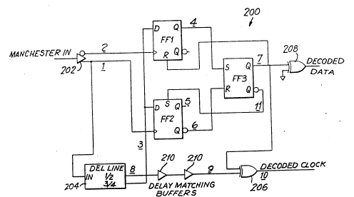
3 An embodiment 200 of the Hanchester decoder
4 clrcuit of the present invention ls shown in FIG. 2. For
S purposes of illustration, a timing diagram of the circuit
200 of FIG. 2 is s~own in FIG. 3, with corresponding signal
7 points indicated in each figure. Referring to FIGS. 2 and
~ 3, a Manchester encoded signal 300 is coupled through buffer
9 circuit 202 to the clocking input of flip-flop FF2 and to
the input of delay element circuit 204. Buffer circuit 202
Il also inverts the encoded signal 300 and provides inverted
1~ signal 302 to the clocking input of flip-flop FF1.
13 Delay element circuit 204 generates delayed ;
14 encoded signals 304 and 306. Signal 304 is delayed by 1/2
of a clock period of the original clock encoded in signal
1~ 300, and signal 306 is delayed by 3/4 of a clock period.
17 The length of the delay depends on the speed at which data
l8 is transferred to circuit 200. For example, at a data
19 transfer rate of 100 Megabits per second, delay element
circuit 204 would be implemented to delay signal 304 by 5.0
21 nanoseconds(ns), and signal 306 by 7.5 ns. Delay element
22 circuit 204 may be implemented using a fixed or programmable
23 delay line circuit. Alternately, if it is desired that
24 circuit 200 be implemented in a fully integrated circuit,
2S delay element circuit ?04 may be implemented as a high-speed
2~ clock circu~t and a multiple-output shift register circuit
27
28
PC~/~S91~/0~6~9
`; 20~240
I to generate the delayed signals 304 and 306.
2 Delayed encoded signal 306 is provided to the data
3 input D o each flip-flop PFl, FF2. Flip-flops FF1 and FF2
are rising edge triggered fl~p-flop circuits. FF1 samples
delayed encoded signal 306 when the inverted encoded signal
302 at its clocking input transitions from a low level to a
7 high level (i.e., on a rising edge of inverted signal 302).
8 Thus in effect FF1 is clocked once for each falling edge of
9 encoded signal 300. FF2 samples delayed encoded signal 306
when the original encoded signal 300 at its clocking input
Il transitions from a low level to a high level (i.e., on a
12 rising edge of encoded signal 300). As described above, it
13 is a property of a Manchester encoded signal that a
14 transition occurs in the midpoint of every data cell due to
the encoded clock signal. The encoded data is represented
1~ by the direction of that transistion. Thus, depending on
17 the data represented in each data cell of the encoded
18 signal, either FFl or FF2 will be clocked by an edge or
19 transition at the midpoint of each data cell. Although
edges are also present at the boundaries of the da.a cells,
21 these transitions do not cause the latched data output of
22 either flip-flop FFl or FF2 to change because the data at
23 the inpu~ of the flip-flop will be the same as the data
2~ previously latched. - :
2S The data signal at the D input of FFl (delayed
2~ signal 306) represents the original encoded signal 300
27
28
~; ,
~09l/0159 l~cr/~ssn/o36~()
206~2~0
1 delayed by 3/~ of a data cell, which is equivalent to 1-1/2
2 code bit cells. If, when a rising edge transition in
3 ~nv~rted signal 302 causes FFl to sample the data at its D
4 input, the sampled data i8 a 1, then it is known that
S original encoded signal 300 has been a 1 for two consecutive
code bit cells and that the decoded data should change from
7 a logical "0" to a logical l'ln Flip-flop FFl accordingly
8 outputs a 1 on its Q output which is coupled to the set
9 control input of an SR flip-flop FF3. This transition,
shown for example by point 308 on signal 310, causes the Q
1~ output of FF3 to be set to a "1". The signal 312 at the Q
12 output of flip-flop FF3 is coupled back to the reset control
13 input of FFl to cause signal 310 at the ~ output of FFl to
14 return to 0 after FF3 has been successfully set. This
lS prevents flip-flop FFl from trying to set flip-flop FF3 at
1~ the same time flip-flop FF2, the operation of which is
17 described below, may try to reset flip-flop FF3.
18 If, on the other hand, the data at the D input of
19 flip-flop FFl is a 0 when sampled, it is known that original
encoded signal 300 has not been a 1 for two consecutive code
21 bit cell^s', indicating that the encoded data has not changed
22 fro~ a logical "0" to a logical "1". Therefore flip-flop
23 FF1 remains in the 0 state (i.e., the signal at ~ o~tput of
24 FFl remains 0) and FF3 is not set. This is the result, for
2S - example, whenever flip-flop FF1 is clocked by an edge at the
2~ boundary of a data cell. -
27
28
~O 91tO1~9~ r(~ 9~)/U3624
, 2~642~0
~ Flip-flop FF2 operates in a simila. manner to
2 reset FF3 whenever the data at its D lnput (delayed signal
3 306) is a 0 when flip-flop FF2 i~ clocked by a rising edge
in signal 300. As in the case of FF1, the data signal at
S the D input of FF2 (delayed signal 306) represents the
original encoded signal 300 delayed by 3/4 of a data cell,
7 which is equivalent to 1-1/2 code bit cells. If, when a
8 rising edge transition in non-inverted signal 300 causes FF2
9 to sample the data at its D input, the sampled data is a 0,
then it is known that original encoded signal 300 has been a
Il 0 for two consecutive code bit cells and that the decoded
12 data should change from a logical "1" to a logical "0".
13 Flip-flop FF2 accordingly outputs a 1 on its inverted Q
14 output which is coupled to the reset control input of SR
IS flip-flop FF3. This transition, shown for example by point
1~ 314 on signal 316, causes the Q output of FF3 to be set to a
17 "0". The signal at the inverted Q output of flip-flop FF3
18 is coupled back to the set control input of FF2 to cause
19 signal 316 at the inverted Q output of FF2 to return to 0
after FF3 has been successfully reset. This coupling back
21 prevents flip-flop FF2 from trying to reset flip-flop FF3 at
22 the same time flip-flop FFl may be trying to set flip-flop
23 FF3.
24 If, on the other hand, the data at the D input of
2S flip-flop FF2 is a 1 when sampled, it is Xnown that original
2~ encoded signal 300 has-not been a 0 for two consecutive code
27
28
~'C) 91/0159~ Pcr/~s9n/036~9
2~6~24~
I bit cells, indicating that the encoded data has not changed
2 from a logical "1" to a logical "0". Therefore flip-flop
3 FF2 remalns in the 1 state (i.e., the slgnal at inverted Q
~ output of FF2 remains 0) and FF3 ~s not reset. This ls
always the result when flip-flop FF2 is clocked by an edge
at a boundary of a data cell.
7 The Q output of flip-flop FF3 is coupled to an
8 input of each of exclusive-OR logic gates 206 and 208. A
9 second input of logic gate 206 is coupled to to the 1/2
I0 clock period delay line of delay element circuit 20Ç by a
I~ plurality of delay matching buffer circuits 210. The
I2 Manchester encoded data signal delayed by 1/2 clock period
I3 (signal 304) is co~bined with the decoded data at the Q
14 output of FF3 (signal 312) to recover the clock Crom the
IS encoded signal.
I~ There is a delay in the decoded data of signal 312
I7 relative to the original data encoded in signal 300. This
I8 delay includes a 1/2 data cell delay which, in recovering
19 the cloc~ signal, is compensated for by the delay of 1/2
clock period in signal 304. There is additional delay in
21 the decoded data-due to signal propagation delays through
22 flip-flops FF1/FF2 and FF3. Delay matching buffer circuits
23 210 compensate for this delay (see signal 317). Preferably,
2~- flip-flops FFl, FF2 and FF3, and delay matching buffers 210
are implemented in a single integrated circuit to minimize
2~ variations in the signal propagation delays of the different
27
28
~V 91/U159~ rCr/~90/036'9
~;: 2~6~2~
I component circuits that might be caused by variationS in the
2 semiconductor pr~cesses used to manufacture the circuits.
3 ECL devices are preferred becau~le of their speed, althoUgh
~ other technologies also may be used. Delay matching buffers
210 can be implemented as desired to emulate the signal
propagation Belays of the flip-flops during operation. If
7 the circuit is implemented using discrete components, delay
8 matching buffers can be implemented using conventional fixed
9 or programmable delay elements.
The clock signal at the output of exclusive-OR
11 gate 206 (signal 318) is inverted with respect to original
l2 cloc~ signal 320. This arrangement is useful for subsequent
l3 circuitry because the rising edge of the inverted clock
14 occurs in the center of each data cell of the decoded data
IS (signal 312), thus giving equal set up and hold times for
1~ clocking the decoded data into additional circuits. Because
17 the decoded data signal 312 is coupled through exclusive-OR
l8 gate 206 to generate the recovered clock 318, the recovered
l9 clock will be delayed from the center of the data cells of
the decoded data by the propagation delay of exclusive-OR
21 gate 206. If it is desired that the propagation delay of
22 exclusive-OR gate 206 be cancelled, the decoded data signal
23 312 can be coupled through an optional delay element, such
2~ as exclusive-OR gate 208 shown in FIG. 2, preferably in the
2S same integrated circuit, to provide a data signal output
2~ having a matching delay.
27
2~
~091/0l'9- r'CI/~S9~)/036~9
-20~240
I Thus a novel circuit for decoding a Manchester
2 encoded digital co~munication ~ignal has been described.
3 One ~killed in the art will nppreciate that the present
4 invention can be practiced by other than the descrlbed
embodiments. For example, flip-flops FFl and FF2 can be
replaced by falling edge triggered flip-flops if the
7 - clocking inputs provided to the two flip-flops are reversed.
8 Further, each flip-flop can be replaced by other latch
9 circuits having cross-coupled logic gates, and alternate
circuitry may ~e used to condition the control signals
Il provided to set and reset flip-flop FF3 to avoid conflict.
12 The described embodiments are presented for purposes of
13 illustration and not of limitation, and the present
1~ invention is limited only by the claims which follow.
17
18
19
21 -
22
23
2-
27
28