Note: Descriptions are shown in the official language in which they were submitted.
20~23
DIF~ERENTIAL FREE SPACE OPTICAL SIGNAL TR~NSMISSION
Technical Field
This invention relates to di~ferential-signal transmission
arrangements and more speci~1cally to optical signal transmission
s arrangements.
Background o~ the In~ention
One conventional equipment design approach in the electronic
arts employs circuit boards on which electronic components are placed, with
the circuit boards being plugged into connectors that are attached to a
0 "backplane". The interconnection of the connectors on the backplane is
called "backplane interconnections" or "backplane wiring".
Although in many respects the point to point connections on a
circuit board are the same as the point to point connections on a backplane,
at the very high pulse rates that current electronic circuits try to sustain
s there is a substantial difference between them. The difference lies in the
longer interconnections on the backplane (on the order o~ magnitude), the
larger physical size of the interconnection paths, and the use of the
connectors. In consequence of these factors~ backplane paths are
characterized by substantially larger capacitances and inductances, and
20 those introduce delay, reduce the path's bandwidth, and require more
powerful drive circuitry. Impedance matching is another problem for
electronic backplanes. Unless the termination impedance of the line and
the input impedances of the taps that receive the signal on the line are
properly matches, substantial distortion and loss can result (e.g., rrom
25 reflections and standing waves).
To overcome those problems, many artisans have turned to
optics, and almost all use fibers. That is, the circuit board is constructed
with a light emitting device (or devices) and means are provided for
coupling the light to a fiber, or a collection of fibers, that carries the light to
30 another circuit board. A receiving (distant) circuit board receives the light from the fiber and detects it.
Operating with optical signals, however, presents its own
problems. Signal level variations, nodal and chromatic dispersion in the
fiber, and other sources of loss and distortion make it necessary to encode
3s the optical signals, if reliable recovery of the original waveform is to be
realized. One common approach, for example, is to encode the data so that
20~4423
- 2 -
the number of l's in the data stream nearly eqllals the number of zeros.
One common level control mechanism is automatic gain control at the
receiver. Still, in some applications this is not suf~lcient tor nol possible),
and edge detection approaches have been used. The overall sensitivity of
5 edge detection, however, is about 3 db less than comparable AC-coupled
designs. Also, significant pulse width distortion is seen in data recovered
with edge detectors. This distortion, and the use of positive feedback in
edge detection receivers, limits the maximum usable bit rate of such
systems.
0 These problems in the detection of optical signals have lead a
few artisans to use differential signal transmission. For example, U.S.
Patent No. 4,316,141 proposes the use of two side-by-side optical Iibers to
transmit an optical signal and its complement. This requires, of course, two
~lbers for each path. In ~J.S. patent application 07/~91,920 filed Oct 2,
15 1990, this requirement is abated by sending the signal and its complement
over the same ~lber, but at two different frequencies.
In the "free-space" environment, a similar approach was taken
by Frank et al. in U.S. Patent No. 4,764,984 issued Aug 16, 1988. That
patent deals with infrared (IR) communication within a room. Therein, IR
20 emitters are placed at the transmitter modules and IR detectors (e.g.,
photodiodes) which are exposed to the radiation are connected to the
receiving modules through fibers. The IR radiation of the transmitting
units is diffused through reflections from walls, floor and ceiling of the room
before being received by the detectors. In other words, the communication
25 of Frank et al. is not directional. To increase sensitivity, Frank et al.
propose to commllnicate bipolar optical signals in the form of two
preselected wavelength IR signals. That requires, of course, twice as many
IR detectors. Differential light detectors are obtained in Frank et al. by
including two detectors for each signal, with each tuned to a different one
30 of the preselected IR wavelengths.
No alignment problems exist in the Franks et al. system because
the IR radiation is diffused. The lack of directionality, however, severely
limits the "channel capacity" of the room because the only way to address a
specific receiver is to either use a receiver-speci~lc pair of wavelengths, or to
35 encode the signal itself with destination information. For that reason,
directed rather than diffused radiation is mGre advantageous.
20~423
- 3 -
A number of directed, free-space, optical interconnection
arrangements are known. For example, U,S. Patent No. 4,720,634 issue(l
January 19, 1988 describes an arrangement where a plurality of circuit
boards are "connected" to a backplane through optical couplings. The
5 backplane is basically a transparent substrate that includes refractive and
reflective areas that are precisely positioned. More speci~lcally, light
emitting devices are placed on the boards and in association therewith the
backplane includes one or more refractive areas that are precisely situated
on the backplane. Light from the device refract off those areas, is
0 collimated through the optical interaction by the grating in that area and is
directed to a precisely positioned reflective area (i.e., a mirror). The
collimated light reflects off the mirror, is directed to other mirrors, as
necessary, and finally is caused to fall on still another precisely positioned
refractive area that focuses the collimated light onto a detector of another
lS circuit board.
Needless to say, this arrangement requires extremely careful and
precise positioning of the various mirrors and refractive areas on the
substrate. It also requires an extremely fine positioning of the circuit boards
relative to the substrate.
In the relatively simple arrangement where the number of optical
connections between the circuit boards is fairly small, the positioning and
alignment problem may be overcome. ~Iowever, in denser utilizations of the
optical backplane, or in an optical computer environment that llses free-
space to pass thousands of closely positioned signal paths (e.g., lûOx 100
2s signals in a 1 cm2 area), a directed communication arrangemen~ such as the
one described in '634 patent is unworkable unless there is extrerne physical
rigidity in the arrangement. Such rigidity can be achieved by substituting
the free-space with glass, for example, but that may not be always possible
or desirable for other reasons. In any event, ~here is an urgent need to
30 alleviate the stringent requirements in free-space optical backplane
applications.
Summary of the Invention
In accordance with the principles of this invenlion, alignment
problems are mitigated in free-space optical signal ~ransmission by the use
35 of differential optical transmission. When the source signals are electronic,a complementary signal is developed electronically, and the signal and i~s
2 ~ 2 3
complement are each applied to a light emitting device. The light of each of
the light emitting devices is collimated with a lens and transmitted to a
receiving lens. The two receiving lenses focus their respective collimated
input onto photodetectors which convert the light to electronic signals, and
s the electronic signals of the two photodetectors are applied to a differentialampli~ler. The two lenses that transmit the signal and its complement form
a transmitting pair, and the two lenses that receive the signal and its
complement form a receiving pair.
The advantage of the above-described arrangement is that the
lo alignment of the receiving lens with respect to the transmitting pair is not
as stringent as before because of the complementary nature of the signal
transmission.
B~ief Description of the Drawin~
FIG. 1 depicts the electrical and optical setup of single path that
15 employs differential transmission;
FIG. 2 illustrates the alignment advantages of this invention;
FIG. 3 depicts a "front view" of an arrangement conforming to
the principles of this invention that is suitable ~or massive, parallel, opticalcommunication such as in a free-space optical computer environment;
FIG. 4 presents an exploded view of the FIG. 3 arrangement; and
FIG. 5 depicts an arrangement conforming to the prin~iples of
this invention that is suitable for more conventional backplane applications.
Detailed Description
FIG. 1 depicts the basic electrical and optical interconnection of
25 a single "dual rail", or differential, signal path. Line 10 receives the input
logic signal and applies it to light emitting device 11 and to inverter 12.
Inverter 12 inverts the logic signal and applies the developed inverse signal
to light emitting device 13. Light emitting devices 11 and 13 may be any
suitable light emitting sources, such as LEDs or lasers. The light emitted by
30 device 11 is collimated in lens 14, and the light emitted by device 13 is
collimated in lens 15.
In accordance with the principles of this invention, lenses 14 and
15 are fixedly attached to a carrier or a platform 22 and the spacing
between the lenses is known to the designer. Similarly, devices 11 and 13
35 are fixedly attached to a carrier 21, with a given spacing between them.
Additionally, carriers 21 and 22 are atLached to each other, such as with
-S- 2064ll23
braces 23, to form a single optical arrangement. Within limits, the spacing
between devices 11 and 13 does not have to be the same as the spacing
between lenses 14 and 15, the light emitting devices do not have ~o be in
the same place or even in parallel planes, and each of the lenses does not
s have to be in a plane that is parallel to its respective lens, or coaxially
aligned therewith. However, meeting these conditions generally simplifies
construction. In fact, platforms 21 and 22 can be a single transparent
substrate with the lenses 14 and 15 being constructed on one surface thereof
in accordance with known planar optics techniques, and the light emitting
0 devices can be attached, or deposited, or grown onto the opposite surface of
the substrate (e.g., surface emitting lasers can be grown, as taught by
Huang et al. in U.S. Patent No. 4,999,842 issued March 12, 1991. Such
construction can be performed with extremely tight precision, and when
that is done, the collimated beans that emanate from lenses 14 and 15 are
15 parallel to each other.
The collimated light beams of lenses 14 and 15 are transmitted
to the receiver, where lens 16 is aligned with the received collimated light of
lens 14, and lens 17 is aligned with the received collimated light of lens 15.
Lens 16 focuses its received collimated light onto a first waist area, and lens
20 17 focuses its received collimated light onto a second waist area. A
photodetector 18 is positioned at the first waist area, and a photodetector
19 is positioned at the second waist area. Neither the waists formed by the
focused beams of lenses 16 and 17, nor the active regions of photodetectors
18 and 19 are e~;plicitly shown in FIG. 1, because the isometric drawing
2s hidden those features.
As with the transmitter, lenses 1~ and 17 are fixedly positioned
onto a carrier 24 and photodetectors 18 and 19 are fixedly positioned onto a
carrier 25. Carriers 24 and 25 are attached to each other. The spacing and
orientation between lenses 16 and 17 on carrier 24is set to correspond to
30 the transmitter design. If the transmitter desi~gn is such that the collimated
beams of lenses 14 and 15 are parallel, then lenses 16 and 17 are positioned
on carrier 24 with a spacing that corresponds to the spacing between the
collimated beams. That is, the spacing of photodetectors 18 and 19 on
carrier 25 and the positioning of carrier 25 vis-a-vis carrier 24is set to align35 the photodetectors with the focus waist areas of lenses 16 and 17, as
indicated above. Again, the arrangement of carriers 24 and 25 and the
2~6~3
-6-
lenses and photodetectors can be constructed on a single substrate using
conventional techniques, as ou~lined above, creating an optical arrangement
that is extremely accurate.
The output of photodetector 18 is applied to one input of a
s differential amplifier 20 (e.g., to the non-inverting input) and the output ofphotodetector 1~ is applied to the other input of the di~ferential amplifier
(e.g., to the inverting input). The output of amplifier 20 forms the output
of the signal connection.
Diagrammatically the arrangement of FIG. 1 is quite simple. In
10 practice, however, the alignment of lenses 16 and 17 with the collimated
beams of lenses 14 and 15 is a major problem. An additional problem is
that in the free-space environment, ambient optical energy (optical noise)
can inject itself between carrier 22 and earrier 24 and be captured by lenses
16 and 17. It turns out that use of the dual rail approaeh, in accordance
15 with the principles of this invention, diminishes the need to precisely align earriers 22 and 24, and also diminishes the effects of optical noise.
FIG. 2, view A, shows a situation where the alignment between
carriers 22 and 24 is perfeet. Cireles 31 and 32 represent the aetive regions
of the photodetectors, and circles 33 and 34 represent the waist areas of the
20 perfeetly aligned beams from carrier 22. Circle 35 represents some ambient
optical signal.
When a logic signal is applied to amplifier 12, there is a
substantial difference between the light intensity of the collimated beams.
In fact, one of the beams may have no light at all. When amplifier 20 is an
2S operational amplifier having an extremely large gain, the output of amplifier20 is basically the sign of the difference in the signals at the amplifier
inputs. That corresponds to the sign of
(Iambient at 31+ I33_ 31) -- (Iambient at 32+ I34_ 3~)
where Iambjent at 31 is the contribution of the ambient light of circle 35 at
30 the detector of circle 31, Iambient at 32 is the contribution of the ambient
light of circle 35 at the detector of circle 32, I33_ 31 is the contribution of
circle 33 at the detector of circle 31 (the intersection of the two circles~, and
I34_ 32 is the contribution of circle 34 at the detectGr of circle 32 (the
intersection of the two circles). Recasting the above equation to
(IambieDt at 31-- Iambient at 32) + (I33_ 31-- I34_ 32)
it becomes clear Ihat as long as the difference in ambient optical energy
7 2n6~23
received by the two photodetectors is smaller than the difference between
the optical energies of the beams as they impinge the photodetector circles
31 and 32, the latter will control the sign and hence the output of amplifier
20.
s In FIG. 2, view B, circles 33 and 34 are misaligned with respect
to circles 31 and 32. That reduces the difference signal to
o~(I33_ 31- I34_ 32). where a equals to 1 when there is complete coincidence
between circle.s 33 and 31. Clearly, as long as oc(I33_ 31 - I34_ 32) iS larger
in magnitude than the difference in the ambient optical energies as
10 addressed above, amplifier 20 still faithfully represents the transmitted logic
signal.
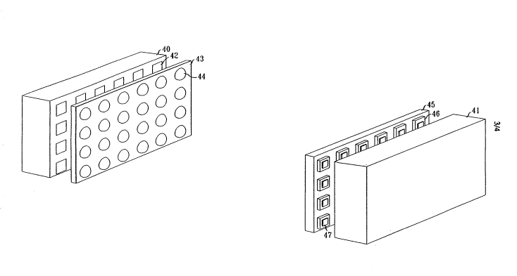
FIG. 3 presents a front view of an optical arrangement in
conformance with the principles of this invention which is useful in an
optical computer environment. FIG. 4 presents an exploded view of the
same arrangement. Block 40 contains whatever electrical and optical
elements transmitting portion of the system requires. The objective is to
transmit selective signals from block 40 to block 41, which contains other
electrical and optical elements. In an embodiment where the signals to be
transmitted exist in electronic form, pads 42 of block 40 are conditioned to
20 output those electronic signals in dual rail mode. That is, the array of pads42 of block 40 is really an array of pad pairs. Block 43 is mated with the
pads of block 40. Block 43 contains an array of light emitting devices, such
as surface emitting lasers, that are grown on the surface facing pads 42.
Block 43 is transparent, with lenses 44 created on the surface parallel to the
2s surface on which the light emitting devices are manufactured. Lenses 44 are
aligned with the light enlitting devices as described above.
An array of collimated beams emanates from block 43 and a
transparent substrate 45 is aligned with the array of collimated beams.
More particularly, transparent substrate 4~ contains an array of lenses,
30 much like the lenses on block 43, and the array of collimated beams is
aligned with those lenses as described in connection with FIGs. 1 and 2. On
a surface parallel to the surface containing the lenses, an array of
photodetectors 46 is applied and positioned as described in connection with
FIG. 1. The outputs of de$ectors 4~ appear on pads 47 which are mated
35 with similarly positioned pads on block 41. Block 41 contains the
operational ampli~lers described in connection with FIG. 1 and all
,
-8- 20~423
subsequent electronic and optical elements.
FIG. 5 depicts an arrangement that is particularly well sllited for
optical backplane applications. Therein, circuit board 50 contains receiving
module 51 and two transmitting modules 52. Each transmitting module
S comprises the transmitting elements shown in FI(3. 1 and, likewise, the
receiving module comprises the receiving elements in FIG. 1. Specifically,
transmitting modules 52 each include an inverter, two light emitting devices
and two collimating lenses. Receiving module 51 comprises two focusing
lenses, two photodetectors and an operational amplifier. In the backplane
10 portion of the FIG. 5 arrangement, the only thing that is needed is means
for directing the collimated beams developed by modules 52 to another card,
such as card 60. That may simply comprise a glass substrate 70 that
includes lenses which are specifically designed to send each transmitted
collimated bean to its destination, much like described by D'Auria in the
15 aforementioned '643 patent. Glass substrate 70 is akin to free-space in some
regards, and is akin to fibers in another regard. It is like a fiber in that
light beams are confined to the interior of the glass substrate until they
reach their specified exit areas. It is like free-space in that a plurality of
different beams, with different entry and exit areas on the glass substrate
20 commingle within the glass substrate. In the context of this invention, I
characterize free-space and the glass substrate as "multiple path-
supporting" media.