Note: Descriptions are shown in the official language in which they were submitted.
VfO 91 /0314.
PCT/US90/04801
-1
HULTI-LAYER CIRCUIT BOARD THAT BUPPREBBEB RADIO
FREQUENCY INTERFERENCE FROM HIGH FREQUENCY BIGNALB
Backaround of the Invention
Field of the Invention
The present invention relates to digital electronic
systems, and, in particular, to circuitry used in digital
computers and the like. More particularly, the invention
relates to the suppression of radiated electrical noise
generated by high frequency signals of such systems.
Description of the Related Art
The circuitry of digital electronic systems is typically
mounted on printed circuit boards. For example, in small
business or personal computers, such circuit boards include a
main system board (often referred to as a mother board) and a
number of smaller circuit boards that are inserted into
connectors on the mother board. Typically, such circuit boards
are multi-layer circuit boards. That is, the connections to
and the interconnections between integrated circuits and other
components on the surface of a circuit board are provided by
metallic traces on the surface layers of the circuit board as
well as on additional traces on inner layers of the circuit
board. In addition, exemplary mufti-layer printed circuit
.boards include layers that are dedicated to a particular
voltage reference. For example, the ground reference (i.e.,
zero volts) may be distributed on an inner layer of the
circuit board. In addition, the primary supply voltage (e. g.,
+5 volts) may also be distributed on a separate dedicated
layer of the circuit board. Interconnections between the
layers of the circuit board are provided by feedthrough
connections (often referred to as vias). In particular,
connections between integrated circuits on one surface layer
and circuit paths on the opposite surface layer are provided
by vias. Similarly', the power and ground connections to the
integrated circuits are provided by vias that are electrically
connected to the respective voltage reference layers.
WO 91/0314.1 ~ ~ ~ n ~ ~ ~ I PCT/fS90/04801
_Z_
Digital electronic circuits generally operate in
synchronism with one or more clock signals that are
distributed to the integrated circuits on the printed circuit
boards. For example, small business/personal computers, such
as computers that utilize the Irate r 80x86 family of
microprocessors utilize a clock signal that is a multiple of
the rated operating frequency of the microprocessor. As a
specific example, a computer based upon an Intele 80386
microprocessor operating at 25 trlfiz utilizes a system clock
signal having a frequency of 50 lgiz. Such an operating
frequency is close to the lower end of the television
broadcast band which begins at 54 l~iz. If the clock signal is
permitted to radiate significant energy, it may interfere with
the operation of television receivers and other radio
frequency communications equipment. Such radio frequency
interference (RFI) is not permitted by regulations promulgated
by the Federal Communications Commission (FCC). Thus, it is
necessary to suppress the radiation of electromagnetic noise
from the clock signal and other signals operating at high
frequencies in order to comply with FCC regulations.
One method of suppressing the radiation of
electromagnetic energy from a digital computer is to shield
the entire computer within a metallic enclosure. Such
metallic enclosures serve the dual purpose of providing
electromagnetic shielding as well as providing structural
support for circuit boards, disk drives and other components
within the computer. However, this method only suppresses
direct radiation to the external environment of the eomputer
and does not prevent radiation of such noise to other signal
lines within the computer. Since it is generally necessary to'
provide signal lines to interconnect a computer to an external
device, such as a printer or the like, the noise generated by
a high frequency signal may be picked up on a signal line and
thus radiated externally to the computer.
In systems where the high , frequency clock signals are
localized on particular cards or on particular portions of a ,
single card, the high frequency clock circuitry on the cards
.. . ._ ::.. .:"x __ ,~.. ,, ;. .:: ,:..,::.,, ..,~: ~.,:: ..... .:. - -.~h~ .
....., ,,.:....
N'O 91/03144 ~ ~ ,~ ~ ~ ~ ~ PCT/L S90/04801
-3-
or card portions can be shielded from other circuits using
conventional shielding techniques such as surrounding the
cards or the card portions with a metallic enclosure. Again,
this is effective only if signal lines carrying the high
frequency clock signals can be isolated from other signals
that pass beyond the boundaries of the shielding enclosure.
Furthermore, the mechanical shielding structures are generally
bulky and add to the overall size of the computer system_ in
which they are used.
l0 Another method that has been utilized is to provide the '
shielding as part of the printed circuit board. For example,
the high frequency clock lines can be positioned on an inner
layer of a circuit board proximate to one or two voltage
reference layers. The voltage reference layer or layers
operate to shield the clock lines to suppress the radiation of
electromagnetic energy. This technique provides significant
improvement over the previously described techniques since the
shielding is applied directly to the printed circuit boards
having the high frequency clock lines. Although this
technique provides substantial improvement in the suppression
of emitted RFI from the clock lines, one skilled in the art
will appreciate that an additional layer of the printed
.circuit board increases the cost of the circuit both in terms .
of material as well as engineering and manufacturing costs.
In addition, the additional layer increases the thickness of
the circuit board. The additional thickness may not be
acceptable, particularly When the printed circuit board has an
' edge connector formed on it. Such an edge connector may be
too large to insert into a conventional card edge connector
used in typical computers. Thus, ~a need exists for a RFI
suppression technique compatible with the existing standards
for printed circuit boards.
Summar~r of the Invention
The present invention is a multi-layer printed circuit
board that is connectable to first and second voltage
reference sources. The printed circuit board suppresses radio
W0 91 /03144 PCT/US90/04801 -
-4-
frequency interference generated by high frequency signals
present in electronic circuitry on the printed circuit board.
The printed circuit board comprises an interconnection layer
which comprises electrically conductive material formed into
a plurality of electrically conductive paths to interconnect
the electronic circuitry on the circuit board.
The circuit board further comprises a first voltage
reference layer connectable to the first voltage reference
source. The first voltage reference layer is positioned in
parallel with the layer of electrically conductive material.
A second voltage reference layer is connectable to the second
voltage reference source. The second voltage reference layer
is positioned in parallel with the first voltage reference
layer.
The printed circuit board of the present invention
further includes means for selectively connecting the first
voltage reference layer to the electronic circuitry and means
for selectively connecting the second voltage reference layer
to the electronic circuitry.
At least~one signal line is formed on the first voltage
reference layer and electrically isolated from the first
voltage reference source. The signal line is shielded by the
first voltage reference layer and the second voltage reference
layer to suppress radio frequency interference between a
signal on the signal line and signals on the interconnection
paths on the interconnection layer.
Preferably, one of the first and second voltage
references to which the corresponding voltage reference layer
is connected is n supply voltage source and the other of the
lirst and second voltage references is a ground reference.
Also preferably, the means for interconnecting the first
voltage reference layer to the interconnection layer and the
means for interconnecting the second voltage reference layer
to the interconnection layer comprise feedthroughs that
penetrate the first and second voltage reference layers and
the interconnection layer.
VfO 91/03144 2 ~ J ~< ~ ~ ~ pL'T/L'S90/04801
-5-
Preferred embodiments of the printed circuit board of the
present invention include ~ second interconnection layer
parallel to the first interconnection layer. The first and
second voltage reference layers are positioned between the
first and second interconnection layers.
In particularly preferred embodiments of the invention,
the circuit board ~ further includes a plurality of
interconnection lines formed in the second voltage reference
layer and electrically isolated from the second voltage
reference source. The interconnection lines in the second
voltage reference layer span the signal line formed in the
first voltage reference layer. The interconnection lines in
the second voltage reference layer are electrically connected
to the first voltage reference source. Preferably, the
interconnection lines in the second voltage z~eference layer
are electrically connected to the first voltage reference
layer via feedthroughs that penetrate the first and second
voltage reference layers.
The circuit board preferably includes a plurality of
capacitors mounted on the circuit board. Each of the
capacitors has first and second leads, with the first lead
electrically connected to the first voltage reference source
via the first voltage reference layer, and with the second
lead connected to the second voltage reference source via the
second voltage reference layer. In exemplary circuit boards
according to this aspect of the invention, a first plurality
of feedthroughs connect the first leads of the capacitors to
the first voltage reference layer and a second plurality of
feedthroughs connect the second leads of the capacitors to the
second voltage reference layer. The first and second
plurality of feedthroughs are positioned proximate to and
electrically isolated from the signal line on the first
voltage reference layer. The first and second plur$lity of
feedthroughs provide additional radio frequency interference
shielding of the signal line on the first voltage reference
layer.
VfO 91/03144 ~ ~ ~ (~~ ~ j ~ ~ PCT/L'S90/0480'
-6-
The present invention is ideally suited for high speed
digital electronic circuits wherein the signal line on the
first voltage reference layer is connectable to a high
frequency signal source, and wherein the first and second
voltage reference layers block the radiation of high frequency
electrical energy from the signal line to interconnection
paths on the first interconnection layer.
Brief Description of the Drawings
Figure 1 is a perspective view of an exemplary multi
layer printed circuit board such as may be used in a computer
system.
Figure 2 is an exploded view of the mufti-layer printed
circuit board of Figure 1 showing two interconnecting layers,
a 5round reference layer and a supply voltage layer.
' Figure 3 is a cross-sectional view of the mufti-layer
printed circuit board of Figures 1 and 2 taken along the lines
3-3 on Figure 2 showing details of the construction of
feedthroughs or vias.
Figure 4 is an enlarged plan view of a feedthrough of
Figure 3 taken along the lines 4-4 in Figure 3.
Figure 5 illustrates an exploded view of the ground
reference layer and supply voltage layer of Figure 3 with a
clock line formed in the supply voltage layer in accordance
with one aspect of the present invention.
Figure 6 is n cross-sectional view of the clock line, the
. supply voltage layer .and the ground reference layer taken
along the lines 6-6.
Figure 7 illustrates an exploded perspective view of the
supply voltage layer and the ground reference layer of Figure
5, further showing the supply voltage.bridge formed in the
ground reference layer to electrically interconnect the supply
voltage across the dock lines.
Figure 8 is a completed mufti-layer printed circuit board
in which the first layer and the ground reference portion of '
1fO 91/0314.; ~ ~ ~ PCT/US90/OJ801
the copper have been partially removed to show the spatial
relationship between the bridges and the cloc:_ lines.
Figure 9 is an enlarged illustration of the area 9 of
Figure 8 which more clearly shows the spatial relationship
between the bridges and the clock lines.
Figure l0 is a cross-sectional view of an exemplary
bridge taken along the lines 10-10 in Figure 9 and also
showing the first, second, third and fourth layers for
clarity.
Figure 11 illustrates the shielding effect provided by
the present invention .wherein the electromagnetic fields
generated by the high frequency clock signal on the clock line
are constrained by the surrounding copper of the supply
voltage and ground reference layer.
Figure 12 illustrates the addition of capacitors which
are connected to a power layer and ground layer.
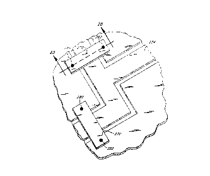
Figure 13 is a pictorial illustration of the waveguide
formed around the clock line in accordance with the present
invention.
detailed Description of the Preferred Embodiment
Brief Review of Structure of Multi-layer Printed Circuit
o s
Figure 1 illustrates an exemplary mufti-layer printed
circuit board 100 which may be used in a computer 104
(represented in part by a phantom outline). Additional
printed circuit boards 106 and 108 are also shown. As
illustrated, the circuit board 100 includes a component
surface 110 onto which are mounted a plurality of electronic
components, such as integrated circuits, transistors,
resistors, capacitors, and the like. The components on the
circuit board are shown pictorially and are designated in
globo by the number 120. The components 120 are
interconnected by a plurality of circuit paths 124 that are
typically formed by etching a copper coating from the surface
WO91/0314.1 r:.~ut~ t(~~~
PCT/L'S90/04801
_g_
110 during the manufacturing process. The copper remaining
after the etching process provides the interconnection paths.
Although only a few circuit paths 124 are shown in Figure 1,
it should be understood that the printed circuit board 100
includes hundreds of interconnection paths 124. It should be
further understood that mufti-layer printed circuit boards,
such as the circuit board 100, further include interconnection
paths on a second surface opposite the component surface 110.
The second surface is not shown in Figure 1. In many printed
l0 circuit boards, additior.:_ components may also be mounted on
the second surface. In ac.-':ition, interconnection paths may be
provided on layers sandwiched between the two surface layers.
When the printed circuit board 100 is to be plugged into
a mother board of the computer 104, or the like, it includes
a connector. Although many different interconnection systems
are available, one of the most common techniques is the use of
card edge connectors which are mounted on the mother board
(not shown). An exemplary conventional card edge connector
130 is illustrated in phantom in Figure 1. The card edge
connector 130 includes a plurality of contacts (not shown)
which provide interconnections for voltages and signals
provided to and generated by the printed circuit boa.-3
components 120. As illustrated, the printed circuit board :.=0
includes an edge portion 140 which has a plurality of
~ regularly spaced metallic fingers 142 that are formed
perpendicular to the edge of the board 100. The fingers 142
engage the contacts of the card edge connector 130 when the
circuit board 100 is inserted into the computer 104. The
fingers 142 are formed by the etching process that forms the
interconnection paths 124, discussed above. The fingers 142
are connected to the components 120 via the interconnection
paths 124.
Figure 2 is an exploded view of the printed circuit board
100 showing four layers 150, 152, 154 and 156. As is known in
the art, each of the layers comprises an insulating substrate,
such as phenolic, onto which is bonded a metallic layer, such
as copper. As discussed above, portions of the copper layer
WO 91/03144 ~ ~ ~ (~ ~ ~ i~ PC1'/US90/04~01
-9-
are etched away from each of the layers to selectively expose
the phenolic substrate. The copper remaining after the
etching process forms the interconnection paths for the
respective layers. It should be understood that each of the
layers is etched separately and then bonded together to form
the composite mufti-layer board illustrated in Figure 1.
As illustrated in Figure 2, the first layer 150 supports
the component surface 110 which includes the interconnection
paths 124. The component surface 110 also includes a
plurality of mounting pads 160 onto which the components 120
(Figure 1) are mounted by soldering or other conventional
methods. Similarly, the fourth layer 156 is formed in a
similar manner to provide interconnection paths. The
interconnection paths are typically on the lower surface of
the fourth layer 156 and are not shown in Figure 2.
The second layer 152 and the third layer 154 in Figure 2
are voltage reference layers. For example, the second layer
152 is advantageously a ground (zero volts) reference and the
third layer 154 is advantageously a power supply voltage layer
(e. g., +5 volts). In typical known printed circuit boards,
the ground layer 152 and the supply voltage layer 154 have
substantial areas of copper remaining after the etching
process to~ provide fairly uniform distribution of the
respective power and ground voltages within the printed
circuit board 100. Basically, the power layer 154 and the
ground layer 152 have copper removed only in areas where
feedthrough connections are formed through the printed circuit
board 100 and the feedthrough connections are to be
electrically isolated from the respective voltage reference.
The foregoing is illustrated in Figure 3 by an exemplary
cross-sectional view of the completed printed circuit board
100 which shows additional details of the construction of each
of the layers. As illustrated, the first layer 150 comprises
a layer 160 of phenolic, or the like, and a thin layer 162 of
copper. The copper layer 162 is etched to form a first
interconnection pad 164 and a~second interconnection pad 166'
to which respective leads of an integrated circuit 120 are
PCT/L S90/04801
WO 91/03144 ~ ~' ~
~.~n4cj~~~
-10-
soldered. The second (i.e., ground reference) layer 152
comprises a layer 170 of phenolic and a thin layer 172 of
copper. A portion of the copper layer 172 is removed to
expose an area 174 of the phenolic layer 170. (The phenolic-
only area 174 is advantageously round and is shown more
clearly in Figure 4.) The phenolic-only area 174 is
' positioned in alignment with the first interconnection pad 164
as shown. Similarly, the third (i.e., supply voltage) layer
154 comprises a layer 180 of phenolic and a thin layer 18~ of
copper. A portion of the copper layer 182 is remove:: to
expose a circular area 184 of the phenolic layer 180. The
phenolic-only area 184 is also positioned in alignment with
the first interconnection pad 164 as shown. Finally, the
fourth layer 156 comprises a layer 190 of phenolic and a thin
layer 192 of copper. A third interconnection pad 194 is
formed from the copper remaining after etching the fourth
layer 156. As illustrated, the third interconnection pad 194
is aligned with the first interconnection pad 164 and with the
phenolic-only areas 174 and 184. The third interconneetion
pad 194 is advantageously the terminus of an interconnection
path 196, as illustrated. The interconnection path 196 may,
for example, electrically interconnect the pad 194 with
another pad (not shown) which is connected via a feedthrough
(not shown) to another integrated circuit (not shown).
.. 25 The first interconnection pad 164 and the third
interconnection pad 194 are electrically interconnected by a
feedthrough (or via) 200 which is formed in a conventional
manner by drilling a hole 202 through the composite circuit
board 100 through the first interconnection pad 164, the
phenolic-only area 174, the phenolic-only area 184 and the
third interconnection pad 194. Thereafter, the hole 202 is
plated with copper, tin lead, or another suitable conductive
material, to provide a continuous conductive path between the
first interconnection pad 164 and the third interconnection
pad 194.
The second interconnection pad 166 is connected to the
ground layer 152 in a manner similar to the previously
W'O 91/03144 ~ ~ ~ ~ i~ y ~ PCT/L'S90/04801
-11-
described connection. However, no phenolic-only area is
formed in the copper layer 172. Rather, the portion of the
copper layer 172 aligned with the second interconnection pad
166 remains intact at a location 210. A phenolic-only area
220 is formed in the copper layer 182 of the supply voltage
layer 154, as described above. Similarly, a pad 224 is formed
in the copper layer 192 of the fourth layer 156. Again, a
feedthrough or via 230 is formed by drilling a hole_232 .
through the second interconnection pad 166, the location 210,
the phenolic-only area 220 and the pad 224. The hole 232 is
plated to provide an electrical path between the second
interconnection pad 166 and the pad 224. It can be seen that
the feedthrough 230 thus formed is electrically connected to
the ground reference layer 152, as desired.
»escrimtion of the Improvement of the Present Invention
As discussed above in the background of the invention,
additional circuit board layers can be provided. For example,
an additional interconnection layer (not shown) can be
provided between the ground layer 152 and the power layer 154.
If the high frequency clock lines are formed on . this
additional layer, they can be effectively isolated from the
other interconnection layers by the shielding effect of the
power and ground layers 154, 152. However, as set forth
above, the additional layer adds to the size (e.g., thickness)
and cost of the printed circuit board. The present invention
provides substantial suppression of the generated radio
frequency noise without requiring an additional layer.
Figure 5 illustrates the ground layer 152 and the supply
voltage layer 154 in accordance with the present invention.
As illustrated, the ground layer 152 and the supply voltage
layer 154 have a substantial amount of the respective copper
layers 172, 182 remaining as in .the prior art. (For
simplicity, the phenolic-only clearance holes for feedthroughs
are not shown in Figure 5.). However, unlike the prior art
printed circuit boards, the copper layer 182 of the supply
voltage layer 154 includes etched portions 250 that defines a
H'O 91/03144 ~ ~ ~ (~~ ~ PCT/US90/0480 r
-12-
plurality of clock lines 254. The clock lines 254 are all
interconnected in Figure 5: however, it should be understood
that additional clock lines can be provided as needed. The
etched portions 250 electrically isolate the clock lines 254
from the remaining portions of the copper layer 182 of the
power layer 154 so that a high frequency clock signal can be
applied to the clack lines 254 without shorting to the supply
voltage reference applied to the supply voltage layer 154.
Figure 6 is a cross-sectional view of the clock line 254,
l0 the supply voltage layer 154 and the ground reference layer
152. The portions of the copper layer 182 of the power layer
154 that are connected to the voltage reference (e.g., +5
volts) are designated by the designator 260. It can be seen
that the clock line 254 is surrounded on both sides by the
voltage reference portions 260 and is positioned beneath the
copper layer 182 of the ground layer 152. Thus, any radio
frequency noise radiated from the clock line 254 is contained
by either the adjacent voltage reference layer portions 260 or
the ground reference layer 172. Thus, the advantages of
shielding the clock lines on a separate layer are provided
without the disadvantages of a separate layer for the clock
lines.
In Figures 5 and 6, the shielding is provided by two
layers having different voltage. potentials. It is preferable
that the shielding be at a single voltage potential. Figure
7 illustrates a further improvement in the embodiment of
Figures 5 and 6 in which the effect of a shield at a single
. voltage potential is provided. As illustrated in Figure 7, a
plurality of conductive bridges 270 are formed in the copper
layer 172 of the ground reference layer 152 by removing
portions of the copper layer 172 to isolate the bridges 270
from the remaining portions of the copper layer 172. The
remaining portions of the copper layer 172 are connected to
the ground reference (e.g. 0 volts) as before and are
designated by the designator~274. Each end of each of the
bridges 270 is connected to the copper layer 182 of the supply
voltage layer 154 via a pair of feedthroughs (not shown in
WO 91/03144 2 O ~ g ~ ~ PCT/US90/04801
-13-
Figure 7 ) so that the bridges 270 are at the voltage potEntial
(e. g., +5 volts) of the supply voltage layer 150.
When the ground reference layer 152 and the supply
voltage layer 154 are positioned proximate to each other in
the completed circuit board 100, as shown in Figure 8, each of
the bridges 270 spans the clock lines 254. In Figure 8, the
first layer 150 and the ground reference portions 274 of the
copper layer 172 have been partially removed to show the
spatial relationship between the bridges 270 and the clock
lines 254. An enlarged portion of Figure 8 is illustrated in
Figure 9 to more clearly show the spatial relationship of the
bridges 270 to the clock lines 254.
Figure 10 is a cross-sectional view taken through one of
the bridges 270 in Figure 9. The view in Figure 10 includes
the portions of the first, second, third and fourth layers
150, 152, 154, 156 for clarity. It can be seen in Figure 10
that a first feedthrough 280 connects one end of the bridge
270 to the copper layer 182 of the power layer 154 and a
second feedthrough 282 connects the other end of the bridge
270 to the copper layer 182. Thus, as further illustrated in
Figure 10, at each bridge 270, the clock line 254 has the same
voltage potential (e. g., +5 volts) above it as it has on both
sides. The feedthroughs 280, 282 provide additional shielding
to the side of the clock line 254. The shielding effect is
illustrated pictorially in Figure 11 wherein , the
electromagnetic field generated by the high frequency clock
signal on the clock line 254 (represented by a plurality of
arrows 288) are shown constrained by the voltage potential on
the ad j scent portions of the supply voltage layer 154 , the
feedthroughs 280, 282, and the bridge 270, thus effectively
suppressing the radiation of the electromagnetic energy.
Since the bridges 270 are spaced apart from each other by .
a short distance (e.g., approximately one-half inch to one
inch in the preferred embodiments), the bridges would apgear
to not provide a continuous shield at~the voltage reference
potential. However, one skilled. in the art will appreciate
that at the frequencies involved (i.e., 50 to 100 l~iz), the
WO 91/03144 ~ ~ ~ j c~ ,_~
7 PCf/fS90/04801
'L ~ J
-14-
bridges :.ave substantially the same effect as a continuous
strip line waveguide. Thus, it is not necessary to provide a
continuous voltage reference portion in the ground reference
layer 152.
Although it is conceivable that the bridges 270 may be
positioned in a manner. so that no gaps exist between adjacent
bridges 270 along the clock lines 254, this is not always
practical. The bridges have the effect of breaking up the
ground reference Layer 152. In addition, each bridge 270
requires a pair of feedthroughs 280, 282 to interconnect them
with the voltage reference layer 154. If rows of feedthroughs
280, 282 are provided along the full lengths of the clock line
254, significant areas of space on the printed circuit board
100 would be unavailable for other use. This problem would
not only be experienced on the ground reference layer 152 and
the supply voltage layer 154, but also by the first and fourth
layers 150, 156 since the feedthroughs 280, 282 also penetrate
those layers.
Although the present invention describes bridges formed
in the ground reference layer 152 to shield the clock lines
254 lying on the supply voltage layer 154, one skilled in the
art will appreciate that this invention could be applied as
well to a bridges formed in the supply voltage layer 154 to
shield clock lines 254 lying on the ground reference layer
. 152. As a further alternative, a portion of the clock lines
254 can be formed in the supply voltage layer 154 and a second
portion .of the clock lines can be formed in the ground
reference layer 152 with the shielding provided by the other
reference layer in each case.
A further improvement in the operation of the present
invention is illustrated in Figure 12. As discussed above the
portions of the ground reference layer 152 between the bridges
270 provide additional shielding: however, these portions are
not at the same voltage potential as the bridges 270. In
order to connect the spaced apart bridges 270 (Figure 8) to
provide the effect of a continuous waveguide over the clock
lines 254, a plurality of 0.01 microfarad capacitors 290 are
WO 91/03144 ~ ~ 6 ~l Q j (~ PCT/L'S90/04801
-15-
mounted on the top surface 110 of the printed circuit board
100. As illustrated in Figure 12, the leads 292 and 294 of
each capacitor 290 are connected to the ground reference layer
152 and the supply voltage layer 154 via a pair of
feedthroughs 296 and 298. Preferably, the capacitors 290 are
located so that the feedthroughs 296 and 298 penetrate the
supply voltage layer 154 and the ground reference layer 152
proximate to the clock line 254. The feedthrough 296 and the
corresponding capacitor lead 292, are electrically isolated
from the ground layer 152 and are electrically connected to
the supply voltage layer 154. Conversely, the feedthrough 298
and the corresponding capacitor lead 294 are electrically
connected to the ground reference layer 152 and are
electrically isolated from the supply voltage layer 154. The
feedthroughs 296 and 298 along the clock line 254 provide
additional vertical shielding between the feedthroughs
connecting the bridges 270. As one skilled in the art will
understand, the effect of the capacitors 290 in the frequency
range of 10-100 I~giz is to provide a low impedance path between
the supply voltage layer 154 and the ground reference layer
152, thus forming an effectively continuous shield over the
clock lines 254.
The overall effect of the present invention is
pictorially illustrated in Figure 13 which represents a
waveguide 300 farmed around the clack line 254. As
illustrated the waveguide 300 comprises the adjacent portions
of the copper layer 182 of the supply voltage layer 154: the
bridges 270: the feedthroughs 280, 282 connecting the bridges
270 to the copper layer 182: the portions of the copper layer
172 of the ground layer 152 between the bridges 270; and the
feedthroughs 296 and 298 that connect the capacitors 290 (not
shown) to the ground reference layer 152 and, the supply
voltage layer 154, respectively.