Note: Descriptions are shown in the official language in which they were submitted.
CA 0206~247 1998-03-03
QUANTUM WELL STRUCTURES
This invention relates to quantum well structures, and in particular but not
exclusively to such structures configured for use as optical modulators.
In the broad field of optical signal processing there are many applications for
high performance optical signal encoding and processing elements. For example, in high
speed optical fibre communications systems, direct modulation of laser sources leads to
undesirable wavelength shifts, "chirp", in the optical output of the laser. One way in
which chirp may be avoided is to cease modulating the laser directly, optical modulation
being achieved through use of a modulator in the optical path of the laser's output. In
the generally less well developed area of optical signal processing, components such as
logic gates, latches, and signal encoders are required. The bandwidth which optical
signals processing and optical communications potentially offer means that there is a
desire for components which operate at high speed, typically switchable at GHz rates,
and preferably switchable at tens of GHz.
The present invention is concerned with such signal processing components,
and in particular with modulators, which comprise quantum well structures. A quantum
well is, in its simplest form, a double heterostructure, with a layer of low band-gap
material sandwiched between two layers of higher band-gap material. Typically the
layers all comprise semiconductors, for example the double heterostructure may consist
of GaAs sandwiched between identical layers of AlGaAs. If the layer of low band-gap
material is suffficiently thin, of the order of 100 A or less, the energy levels in the valence
and conduction bands becomes quantised, and the structure is referred to as a "quantum
well".
While single quantum wells do exhibit measurable quantum effects, the
intensity or strength of the effects can be increased by increasing the number of
quantum wells. Several, typically tens or many tens or hundreds of quantum wells are
formed in a multilayer structure, which structures are referred to as "multiple quantum
wells", or "multiple quantum well" ("mqw") structures.
The basis behind the use of quantum well structures as modulators is that
they can exhibit large changes in their optical absorption coeffficient on the application
of an electric field.
In devices such as QW modulators, utilising excitonic effects, the exciton of
most significance is that involving the n=1 heavy hole. In this specification, unless the
context clearly requires otherwise, we refer to the n=1 heavy hole exciton.
CA 0206~247 1998-03-03
;
Our own interpretation of the accepted explanation of this phenomenon will
now be given with reference to Figure 1 which shows, schematically, the behaviour of
a conventional quantum well structure. The structure will be assumed to consist of a pair
of GaAlAs layers 2, 2' with a GaAs layer 1 therebetween. Thin solid lines 3 and 4
5 indicate respectively the valence band maximum in bulk GaAlAs and GaAs. Thin solid
lines 5 and 6 similarly indicate the conduction band minimum in bulk GaAlAs and GaAs
respectively. However because the GaAs layer is thin enough to provide quantum
confinement of the electrons and holes there is an increase in minimum energy for them
both. The new minima, the quantum well minima, for the electrons and holes are shown
10 as broken lines 7 and 8 respectively. Note that in Figure 1 electron energy increases
towards the top of the Figure and hence hole energy increases as one moves down the
Figure. With no applied field the resultant energy gap 9 is greater than that of the
equivalent bulk GaAs. Typical probability density distributions of electrons and holes in
the well are indicated by 10 and 11. The probability density distributions are pseudo-
15 Gaussian and centred on the mid-point of the well.
Figure 1 b shows, schematically, the effect of applying an electric field acrossthe layers of the well of Figure 1a. With the field applied, the shape of the potential
energy well seen by the electrons and holes changes dramatically. As a result of the
changed band edge variation the probability density distribution of electrons follows the
20 drop in minimum conduction band energy and hence moves to the right (the positive
potential side) in Figure 1b. Similarly, the hole distribution follows the fall in valence
band minimum (hole) energy and hence moves to the left (the negative potential side)
in Figure 1b. The result is that the band gap shrinks. This is the so-called quantum-
confined Stark effect. The change in band gap of course causes a shift in the absorption
25 band edge, increasing absorption at lower photon energies (a red shift). Thus a
quantum well device can be used as a modulator for wavelengths in the region of the
band edge.
Unfortunately, in addition to the desired band edge shift there is a significantreduction in the absorption coeffficient when a field is applied. In US 4,826,295 the
30 absorption coefficient for photon energies greater than the no-field band gap is estimated
in one example to fall from about 2000 cm~1 in the no-field case to about 300 cm~1 in
the with-field case. For photon energies just below the no-field band gap, but above the
relevant with-field band gap, the absorption coefficient is estimated in US 4,826,295 to
CA 0206~247 1998-03-03
rise from less than 10 cm~~ with no field to about 300 cm~1 with an applied field. While
not preventing the use of quantum well structures in practical modulators, the fact that
an absorption coefficient drop is associated with the desired field-induced band edge
shift is nevertheless a disadvantage of known quantum well optical devices.
The present invention seeks to provide quantum well structures in which field-
induced band edge shifts can be achieved without a significant accompanying change
in absorption coefficient.
The present invention seeks to provide quantum well devices, and in
particular quantum well modulators, which have a reduced sensitivity to small variations
in well width and/or reduced sensitivity to electric field nonuniformities within the devices
during their operation.
The present invention also seeks to provide quantum well devices of the type
described, which devices have operating voltage requirements lower than those ofcomparable prior art devices.
In European patent application 0324505 there is described a second-
harmonic generator or frequency doubler which comprises a quantum well structure.
According to 0324505, the conversion of radiation of angular frequency ~ to radiation
having an angular frequency 2w, in a non-linear material, has an efficiency proportional
to the square of that material's non-linear receptivity ~ (2) In EP 0324505, a dipole
moment is induced in a quantum well structure, ~ ~2) of that structure being proportional
to the size of the dipole moment. In the first embodiment in '505, the well comprises
120A of GaAs sandwiched between AlAs barrier layers. Several such wells, together
with thicker, charge separating layers of AlAs, form the intrinsic region of a p-i-n
structure. By applying an electric field across the layers, the centres of gravity of the
wave functions of the electrons and holes in the well shift, creating a dipole moment.
With an applied field of unspecified strength, yl (2) of the aforementioned structure is said
to be 400 times as large as that of LiNbO3, and 5000 times as large as that of KDP.
The angular frequency, w, of the radiation to be up-converted is chosen to
satisfy the relation 2hw~ Eg, where Eg is the bandgap of the well material (here GaAs,
whose bandgap is 1.42 Ev at 300K).
In place of the AlAs in the barrier layers, AIxGa1 xAs can be used, and this
permits the construction of a waveguiding quantum well structure, further increasing the
efficiency of conversion.
CA 0206~247 1998-03-03
As an alternative to the formation of a dipole as the result of an applied field,
an embodiment is proposed in which a dipole is formed by varying the composition of
the well from (InAs)1 x(GaAs)x to (GaSb)~ y(GaAs)y across the well width, AlAs barrier
layers being used. This structure is suggested to give second harmonic generation with
5 an effficiency as high as that in the first embodiment described above. Also it is stated
that this graded structure allows one to dispense with the electrodes and power source
used in the first embodiment, since the application of an electric field is no longer
necessary.
Further embodiments in '505 include a modulator for modulating the bias
10 electric field, thereby modulating (2) and hence modulating the harmonic wave.
In a further embodiment a filter is provided at the optical output of the qw
structure, the filter passing the second harmonic wave and blocking the low frequency
input signal. This embodiment is also proposed for use in combination with the
modulator or the graded-composition well.
Nowhere in '505 is there any suggestion that any advantage is to be obtained
for applications other than second-harmonic generation by having a quantum well
structure having a compositionally-induced dipole.
Nowhere in '505 is there any suggestion that there is any merit in providing
a quantum well structure having a compositionally-induced dipole with electrodes. In this
20 connection it should be noted that in '505 it is suggested that with a graded structure the
dipole is fixed and hence 5~ (2) is fixed, while modulating the bias voltage on a non-
graded well structure - where ~ (2) iS dependent on the size of the applied field, results
in a desired modulation of the second harmonic signal through modulation of yl (2)
In their paper in Joumal of Applied Physics, Vol. 62, No. 8, pp3360-3365,
25 Hiroshima and Nishi describe a graded-gap quantum well (GGQW) structure in which
there is an effective 'internal' electric field which concentrates the carriers on the same
side of the well in both the conduction and valence bands. The authors note that such
a structure can be realized by varying the alloy composition in the well layer so that the
band gap varies linearly within the well. The paper deals with a theoretical analysis of
30 the so-called quantum-confined Stark effect with particular attention being paid to
excitonic effects. The structure on which their theoretical analysis is built is a GGQW
comprising an AIxGa1 xAs well layer,1 ooA thick, in which the aluminium content x varies
from 0 to 0.15 along the growth direction, and Al06GaO4As barrier layers. The authors
note that the electron and light-hole envelope functions for various applied field
CA 0206~247 1998-03-03
conditions are nearly symmetric and are less effected than the heavy-hole envelope
function by an external applied field.
It is interesting to note that Hiroshima and Nishi are concemed only with their
linearly-graded gap quantum well structure, which in their words "has an effective
"internal" electric field which concentrates the carrier on the same side of theheterointerface in both the conduction and valence bands". Nowhere do they suggest
that pushing the electrons and holes to the same side of the well with a built-in field is
a bad idea or that there is anything to be gained by building a structure in which the
electrons and holes are pushed to opposite sides of the well by a built-in field. The
authors are not concemed with establishing a structure which inherently produceselectron-hole pairs as dipoles, and do not teach towards such a concept. From our own
study of the paper, it appears that the structure which they describe does produce a
small inherent dipole, probably with a dipole moment of no more than 5A.
Preferred embodiments of the present invention will now be described, by
way of example only, with reference to the accompanying drawings in which:
Figure 1(a) is a schematic energy band diagram for a single quantum well
with zero applied electric field;
Figure 1(b) is a schematic energy band diagram for the quantum well of
Figure 1 (a) with an applied electric field;
Figure 2 is a schematic energy level diagram for a single quantum well
according to the present invention;
Figure 3 is a schematic energy level diagram for a single quantum well
according to the present invention, the well consisting of a layer of essentially gallium
antimonide, and a layer of essentially indium arsenide, the barrier layers comprising
aluminium antimonide;
Figure 4 is a schematic cross-section through a tuneable Bragg reflector
according to the invention; and
Figure 5 is a schematic energy level diagram for a single, non-optimum,
quantum well according to the present invention.
The invention in its broadest sense is perhaps best explained by reference
to the behaviour of a conventional quantum well structure such as that represented in
Figures 1 (a) and 1 (b). The following explanation or description of the behaviour of such
a conventional quantum well structure is unusual, but is believed to make explanation
of the present invention much easier. The non-expert reader will no doubt be thankful
for the general absence of calculus!
CA 0206~247 1998-03-03
.
Consider an electron-hole pair in its ground state in a conventional symmetric
square QW. In the absence of an applied or built in field the charge density (10 and 11 )
of both the electron and hole will have its 'centre of gravity' coincident with the centre of
the well. The energy needed to create this ground state, ie the photon energy needed
5 to promote the electron from the top of the valence band to the bottom of the conduction
band, is just the bandgap, 9, of the QW. (We neglect the electrostatic attraction between
the electron and the hole that gives rise to the formation of excitons since this plays only
a minor role in the so called quantum confined Stark effect). When an electric field is
applied to the quantum well the energy needed to create the above mentioned electron
10 hole pair, the band gap energy, will change; and subsequently there will be
electroabsorption. So all we need to do to understand how the QW band gap changes
with applied electric field is to understand how the minimum energy needed to create an
electron hole pair changes in the same circumstances.
To find how the energy of an electron hole pair changes when an electric
15 field is applied we can picture the pair as a polarisable atom. When the field is applied,
the positively charged hole will move to the down field side of the well while the
negatively charged electron will move in the opposite direction towards the up field side
of the well. The 'centres of gravity' of the two charge distributions will no longer be in
the same place and consequently an electric dipole moment will have been induced.
20 Elementary eleul,ustalics tells us that the energy of an electrically neutral system with
a dipole moment, p, in a field, F, is just -pF. Hence when the dipole moment is in the
same direction as the field, as in our case, then the system has a lower energy in the
presence of the field than in its absence. Hence the minimum energy needed to create
an electron-hole pair, ie the band gap, decreases with increasing applied field. There
25 is an associated red shift and decrease in height of the absorption edge. The decrease
in height comes about because the electron and hole are separated by the field and it
is more diffficult for the light to create spatially separated electron hole pairs then electron
hole pairs in which the carriers have the same charge distributions.
While the above arguments give a qualitative understanding of the quantum
30 confined Stark effect, it is not quantitative. To make the arguments quantitative, which
is important for an appreciation of some of the advantages of the invention, we must
include the work done on the electron hole pair during its formation. Again elementary
electrostatics tells us that the work done in creating dipole is +(apF2)/2, where ap is the
CA 0206~247 1998-03-03
polarisability of the electron hole pair. This raises the energy of the dipole by the same
amount. So the change, ~E, in the energy of the electron hole pair due to the presence
of the field is
I~E =-pF + (apF2)/2 (1)
5 But, by the definition of the dipole moment and the polarisability,
p=apF (2)
so that
I~E =-(apF2)/2. (3)
Note that the shift in the absorption edge (which is to the red) is the same regardless of
10 the direction in which the field is applied.
We have seen that the shift in the absorption edge varies as the square of
the total field experienced by the electron hole pair. This field will in general be a
combination of built-in and applied fields. Ideally, one would want this total field to be
the same for all the quantum wells in a device such as a modulator so that the
15 absorption edges of the wells move in unison, and an optimum extinction ratio results.
However, there will inevitably be field nonuniformities and hence corresponding
variations in the shifts in the absorption band edge. These shifts in the absorption band
edge throughout the device will be magnified by the quadratic dependence on the field,
the result being that the fractional variation of ~E from well to well will be double the
20 fractional variation in F from well to well.
Inhomogenities in the electric field are by no means the only problem.
Variations in well width, L, can also produce problems. When one evaluates the
polarisability of a conventional quantum well one finds that it varies as L4. Hence any
fractional variation in the width of the quantum wells in a surface modulator (that is one
25 in which light propagates in a direction normal to the planes of the quantum well layers)
will give rise to a fractional variation in the bandgap 4 times that in the well width. This
results in a smearing of the absorption edge when an electric field is applied additional
to the smearing already present due to inhomogenities in the applied field.
It is clear that these properties make the design and fabrication of modulators
30 and in particular surface modulators using conventional quantum wells particularly
demanding.
The preceding analysis of the operation and deficiencies of conventional
quantum well structures is the result of our appreciation of the potential benefits offered
CA 0206~247 1998-03-03
by the present invention. As far as we are aware, no - one has previously considered
or described the operation of quantum well structures in terms of electrostatics. We
have realised that the problems arise in the conventional quantum well devices such as
modulators because the electroabsorption is essentially the result of two conflicting
5 processes. On the one hand, the tuming on of the field raises the energy of the system
by performing work on it during the creation of the dipole. On the other hand, the
presence of the field lowers the potential energy of the system by virtue of the presence
of the dipole. Looked at in this way it is not surprising, therefore, that the end result, the
shift in the absorption edge, is sensitive to parameters such as F and L. There is also
10 another unsatisfactory aspect. In order to shift the absorption edge one must create a
dipole. In so doing one makes absorption more difficult and so one is in fact degrading
the very property one is trying to exploit, namely the high band edge absorption!
Having first realised, with the help of our electrostatic approach, that the
applied field is changing the band gap as the result of first forming a dipole and then
15 acting on the dipole to lower its energy, we further realised that we could overcome
many of these problems by producing asymmetric QW structures which automaticallyproduce electron-hole pairs as dipoles.
If a suitable asymmetric QW is used, then an electron-hole pair will already
have an intrinsic dipole moment, pj, and there is no need to create one; the 'centres of
20 gravity' of the electron and hole charge distributions will naturally be in separate places.
Additionally, if one uses a narrow well then, if the well is narrow and deep enough to
bind the carriers strongly, the polarisability will be small. To a good approximation, the
change, ~E, in the band gap in the presence of a field, F, is given by
AE =-pjF (4)
25 ie equation (1 ) with ap = 0.Equation (4) immediately shows us the benefits of QWs which
produce electron-hole pairs as dipoles. Because pj is independent of electric field then
~E depends only linearly on the field. Since pj is essentially a displacement between
the 'centres of gravity' of two charge distributions one expects it to vary more nearly
linearly with well width, L. We now see that the shift in the absorption edge is much less
30 sensitive to variations in electric field and well widths than the conventional QW. A much
'cleaner' electroabsorption characteristic is therefore expected of suitably designed QW
and MQW structures.
CA 0206~247 1998-03-03
There is also another advantage in using wells which inherently produce
electron-hole pairs as dipoles which is revealed on closer examination of equations (d)
and (4). Rewrite (3) in terms of the dipole moment, Pc1 induced in the conventional QW
/~E =-(pCF)/2 (5).
We see that for a given l~E, the dipole Pc induced in the conventional QW is
twice as large as pj, the intrinsic dipole needed in the asymmetric QW. This means that
when the field is applied, the intrinsic dipole QW has a superior absorbance per well,
because the electron and hole charge distributions have more overlap. The absorbance
per micron of material is further increased if one uses narrow wells because one can fit
more narrow wells per micron than those of conventional thickness. Additionally, for
fixed ~E, and P(=Pc=Pi) the field (and thus the voltage) required with a fixed dipole
structure is half that needed for a conventional structure.
The arguments presented above show that the desirable features of the
electroabsorption characteristics of modulators and in particular surface modulators
containing conventional symmetric quantum wells are inherently vulnerable to
nonuniformities in well widths and applied fields. As such the engineering of modulators
using such quantum wells is diffficult. Simple arguments suggest that asymmetricquantum wells which produce electron-hole pairs as dipoles provide (1) a way of
reducing modulator susceptibility to these nonuniformities and (2) an enhanced extinction
ratio, or alternatively the same extinction ratio as in the conventional device but with
lower voltages.
For optimum results where one is not constrained to use very low (i.e. 1 to
5 volts) operating voltages we believe that the well width, that is the width of the region
which will hold both electrons and holes, should be no more than about 50 A. This
region will of course be made up of at least two materials, since at least two offset
bandgaps are needed to ensure the spatial separation of the carriers needed for the
creation of the intrinsic dipole moment. The different materials for the well region will,
in many cases, be ternaries or quaternaries, or one or more of each, formed fromessentially the same elements.
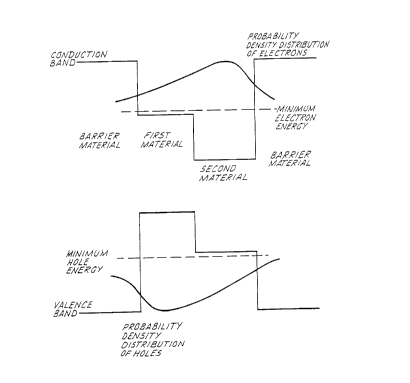
Figure 2 illustrates schematically the insensitivity of carrier probability density
distribution with respect to minimum energy level. The presence of the deep wells in the
conduction and valence bands skews the carrier distributions even though the minimum
energy levels are "above" the energy ranges of the deep wells.
CA 0206~247 1998-03-03
- 10-
As mentioned above, to ensure low polarisability, deep wells are necessary
for the electrons and holes.
Where the QW structure is to be driven with low applied voltages, for
example less than about 5 volts, optimum performance will generally be achieved with
somewhat wider wells, for example up to about 100A.
Materials
As will by now be clear, the quantum well structures according to the
invention have conduction band profiles which tend to push the electrons in the well to
one side of the well and valence band profiles which tend to push the holes in the well
10 towards the opposite side of the well. One suitable materials system uses aluminium
antimonide (AlSb) barriers with quantum wells formed of gallium antimonide (GaSb), for
hole confinement, and indium arsenide (InAs), for electron confinement. A schematic
energy level diagram of such a quantum well structure is shown in Figure 3. The solid
lines in Figure 3 represent the conduction and valence band levels for the bulk
semiconductors and illustrate the overlap between the conduction band in InAs and the
valence band in GaSb. However, as explained previously, quantisation of the energy
levels when there is 'quantum confinement' leads to an increase in the minimum
allowable energies for electrons and holes in the well, and hence the overlap disappears.
In particular electrons in InAs are very light and hence are easily quantised. Typical
energy levels for the quantum well are indicated by the broken lines.
Of course the constituent compounds, and elements, of this system can
readily be alloyed, and hence device characteristics can be tailored, for example by
selecting alloy compositions for the quantum well layers which give the desired bandgap.
In particular there are advantages in forming the hole confining region from an InAs rich
alloy of InAs and GaSb.
Of course, as those skilled in the art will appreciate, while quantum well
structures according to the present invention are preferably based on the above
described materials system, there are other materials systems which could be used.
One such system which is capable of providing quantum well structures according to the
invention is that comprising indium antimonide (InSb), cadmium telluride (CdTe) and
mercury telluride (HgTe). It is known to use HgTe and CdTe alone in quantum wellstructures, for example see the paper by Guldner et al, in Physics Review Letters, Vol.
51,p907,1983, but not in combination with InSb. Fortunately InSb is lattice matched
to CdTe, so its incorporation into the known two component system is possible. CdTe
would provide the barrier layers. Bulk InSb has only a small band gap, 0.2eV, and bulk
CA 0206~247 1998-03-03
.
HgTe has no band gap. Quantum confinement gives rise to a band gap in HgTe, and
causes the band gap of InSb to increase.
Preferably, with the proposed GaSb/lnAs/AlSb quantum well structures a
GaSb substrate is used. The reason for this choice is that both InAs and AlSb are
5 slightly imperfectly lattice matched to GaSb, but in opposite senses. If appropriately
dimensioned InAs and AlSb layers are grown alternately on GaSb, the strains tend to
cancel each other out, with the result that greater overall thicknesses can be grown.
Also, it should be noted that Figure 3 illustrates what is in effect the simplest
realisation of the invention: there are just two regions in the quantum well, one for
10 confinement of holes, the other for confinement of electrons. While of course it is
generally preferable, from the point of view of crystal growth, to keep the number of
components and the number of different layer types to a minimum, it may still be found
worthwhile to incorporate more components and/or more different layer types to enable
the use of different alloy systems or to permit the production of more complex structures
15 which have good electron and hole confinement and separation. Barrier widths of 50-
100 A are typical.
Normally the barrier layers will comprise a simple semiconductor, but there
may be applications where it is advantageous to use alloyed semiconductors or even
near insulators for the barrier layers. The advantage of using simple semiconductors is
20 that they are easier to grow well.
While barrier widths will normally be in the range 50 to 100A, the optimum
width for any particular application should be determined by routing experimentation.
The barrier width should be sufficient to at least substantially prevent tunnelling between
wells when the working potential is applied, the object being for adjacent wells to be
25 unaffected by each other. Because the probability of tunnelling is determined by the
effective barrier height, thinner wells will in general need thicker barrier layers, all other
things being equal. Likewise in materials systems where the effective barrier heights are
necessarily low, it will generally be necessary to use barrier layers thicker than those
required in the GaSb/lnAs/AlSb system. It is undesirable to use barrier layers which are
30 thicker than necessary, since excess barrier thickness will reduce the field intensity
'seen' by the quantum wells for any particular applied voltage. An additional and
significant disadvantage of excess barrier thickness is that it is wasteful of epitaxial
growing time and ability - generally it would be more useful to grow a multiple quantum
well structure comprising a greater number of wells.
CA 0206~247 1998-03-03
. ~
The following examples based on the InP/GalnAsP/lnGaAs system are
included to show how it is possible to create significant and useful dipole moments even
with materials which do not provide very deep wells. In terms of the invention, this
materials system is very much non-optimum, but nevertheless applying the invention to
5 this 'everyday' materials system does give appreciable advantages. Well widths of 60A
are assumed in these examples, but this is not critical.
Examples
For two-part quantum wells of GalnAsP and InGaAs between InP barriers,
10 calculations of dipole moments for electrons and holes for different phosphorus contents
in GalnAsP. An InP substrate was used, the InGaAs being lattice matched to InP.
1. For InGaAs sub-well of width 25A, with a GalnAsPy sub-well of width 25A.
Molar Concentration Hole Electron Difference
of P Dipole Dipole Dipole
Moment A Moment A Moment A
0.05 2.59 0.54 2.05
0.10 4.85 1.10 3.75
0.15 6.63 1.68 4.95
0.20 7.95 2.28 5.67
0.25 8.91 2.90 6.01
0.30 9.62 3.52 6.10
0.35 10.17 4.17 6.00
0.40 10.59 4.82 5.77
0.45 10.92 5.49 5.43
0.50 11.20 6.15 5.05
0.55 11.42 6.82 4.60
0.60 11.61 7.49 4.12
0.70 11.92 8.82 3.10
0.80 12.15 10.10 2.05
0.90 12.34 11.34 1.00
CA 0206C7247 1998-03-03
.
- 13-
2. For 50A sub-well widths: 50A InGaAs, 50A GalnAsPy.
Concentration Dipole Moment
of phosphorus Difference A
0.02 5.499
0.04 9.614
0.06 12.140
0.08 13.521
0.10 14.187
0.12 14.417
0.14 14.374
0.16 14.156
0.18 13.821
0.20 13.409
0.22 12.943
0.24 12.442
0.26 11.920
0.28 11.386
0.30 10.846
3. For sub-wells of 17.58A (6 mono-layers) GalnAs, and 41.02A (14 mono-
layers) GalnAsP.
Molar Dipole
Concentration Moment
phosphorus Difference
A
0.2 10.352
0.25 11.602
0.30 12.139
0.35 12.189
0.40 11.909
0.45 11.397
CA 0206~247 1998-03-03
- 14-
Figure 5 shows the band-gap and notional probability density distributions for
electrons and holes for this structure with a molar concentration of phosphorus of 0.40.
The notional displacements of the 'centres of gravity' of the hole and electron
distributions are shown as stars.
As with other QW modulators, modulators according to the present invention
will routinely be in the form of a PIN structure with the quantum wells in the intrinsic
region. Also conventional is the use of charge separating layers of intrinsic material to
each side of the QWs, to ensure uniformity of field. The charge separating layers are
conveniently formed of the material used in the barrier layers of the QWs, and anyway
are chosen to have a bandgap greater than that of the low gap material in the QWs. On
either side of the intrinsic region there are respectively provided a p and an n region to
which the device's electrodes are connected. Typically, metal electrodes forming ohmic
contacts with the p and n regions are used.
In a further embodiment the invention provides a tuneable Bragg reflector
comprising multiple multiple-quantum-well stacks, each mqw stack comprising quantum
well structures according to the invention and grown in one sense, alternate mqw stacks
having the growth sense reversed. By growing each mqw stack of quantum wells grown
in one sense, that is with their intrinsic electron-hole dipoles disposed in the same sense
(poled), and then growing the next mqw stack with the intrinsic electron-hole dipoles
poled in the opposite sense, and so on, a structure is created in which, on application
of a suitable potential thereacross, the refractive indices of alternate layers can be varied
in opposite directions.
An example of such a structure is shown schematically in Figure 4. Such
structures are useable as tuneable Bragg reflectors in either waveguide or surface
configuration, the latter configuration being illustrated in Figure 4. In the structure
illustrated, which is designed for normal light incidence, the mqw stacks are each of a
thickness approximately equal to one quarter of the device's operating wavelength - that
is, each layer has a thickness of ,I/4n, where n is the refractive index of the layer at the
wavelength ,1. The operating wavelength can be near the band-gap -equivalent
wavelength, in which case there can be strong refraction but with the possibility of
absorption, or longer wavelengths can be used with correspondingly reduced refraction.
An electric field is applied, normal to the planes of the layers, by means of electrodes
on the end faces 50, 51 of the structure. A material such as indium tin oxide ITO, which
CA 0206C.247 1998-03-03
.
- 15-
is electrically conductive and which transmits light, may be applied to the end faces of
the structure for use as electrodes. More generally, metallic contacts will be applied to
the end faces. The number of layers in each stack and the number of stacks in the
structure are not critical and the optimum numbers for any particular application may be
5 determined by routine experimentation. The upper limit on both numbers will in general
be set by the maximum thicknesses which can be grown while maintaining good epitaxial
growth, by the operating wavelength range, and by the requirements for the driving field
and for optical performance.
As those skilled in the art will be aware, in order to ensure electric field
10 uniformity, it is desirable to provide charge separating layers of intrinsic material between
the electrodes and the mqw stacks. Conveniently this intrinsic material may have the
same composition as the barrier layers in the MQWs. Schottkey contacts can be
provided to the structure using appropriate contacts. Alternatively, a PIN structure may
be used, the mqw and charge separating layers constituting the intrinsic region thereof.
Typically each mqw stack would comprise between 10 and 100 quantum
wells, more typically 25 to 50, for example 40. Typically there will be between 3 and 50
stacks in total, more typically between 10 and 40, for example 30.
Tuneable Bragg reflectors in waveguide configurations can readily be
constructed, although of course the layer thicknesses and numbers and number of
20 stacks will in general differ from those used in the above described surface configuration.
Tuneable Bragg reflectors according to the invention may conveniently be
produced using the InP, InGaAs, GalnAsP material system. By selecting GalnAsP
compositions with phosphorus contents which give the largest dipole moments for the
well widths chosen, good optical performance can be obtained. Examples 1, 2 and 3
25 above give an indication of suitable well-widths, compositions and phosphorus contents.
Bragg reflectors comprising QWs formed from the other materials systems
set out above can be expected to provide performance significantly improved over that
obtained with the InP, InGaAs, GalnAsP system.