Note: Descriptions are shown in the official language in which they were submitted.
2~ s7
OUTPUI' AMPLIFIER
BACKGROUND OF THE l~l V ~:N~ oN
The present invention relates to amplifiers
used at the end of a signal path for providing an
amplified signal to an output device and, more
particularly, to such amplifiers which are to operate
with a low quiescent current and also be capable of
operating with a low supply voltage.
There are many situations in which electronic
lo circuits must operate with only a low supply voltage
being available thereto. In battery operated equipment,
particularly, not only is the supply voltage often low,
but also ;ni ;zing power dissipation is very important
to lengthen the life of the battery or batteries used.
Yet some of these situations require an o~ L amplifier
circuit which can deliver a considerable amount of power
to the load device, perhaps aided by some capacitive
storage provided across the power supply.
In these circumstances, the out~u~ amplifier
type is often chosen to be such that the output
transistors therein carry little or no current in the
absence of an input signal to the output amplifier
stage. This minimizes power dissipation during such
conditions to thereby reduce the drain on the power
supply and so leads to improved amplifier e~ficiency in
converting power from such a supply to signal power.
One type of equipment where this has become
increasingly important is in hearing aids, these having
begun as a chest-worn package of electronics with a lead
to an output device worn in the ear. The next major
change was to a behind-the-ear electronics package, and
then to an in-the-ear package and, finally, to an
in-the-canal package. The reduction in size of the
~ 57
electronics package, including the battery power supply,
to make such a transition in the locations on their
person at which users of such hearing aids carry that
equipment is quite remarkable. Microphones, speakers or
receivers, batteries and electronic circuitry have all
undergone varied but quite significant size reductions
to make this possible.
However, further reductions in the physical
size of these various portions of a hearing aid -are
desirable to increase benefits to the users thereof. A
major difficulty in reducing the geometrical volume of
the associated electronic circuitry has been the nl h~r
of external capacitors nee~e~ in connection with output
amplifier, the r~ -;ning circuitry of which is provided
in a monolithic integrated circuit chip. Although such
capacitors have also been reduced in size, they together
still present major difficulties in miniaturizing
hearing aid packages sufficiently to be insertable into
smaller ear c~n~lR. Thus, there is desired an ouL~uL
amplifier circuit requiring little quiescent current
which is capable of being operated at a low supply
voltage, and which, as formed in a monolithic integrated
circuit chip, reduces the number of external capacitors
required to be used therewith.
SUMMARY OF THE INVENTION
The present invention provides an amplifier
having a pair of controlled current generatihg means
each with an output impe~nce means that is electrically
connected to the other, a pair of ouL~L controllers
each of which is across a corresponding one of the
output ; ~ nce means, and a pair of feedback means
each connected from a corresponding one of the output
controllers to a corresponding one of the controlled
2~4 ~7
current generating means. The output impedance means of
each of the controlled current generating means has a
portion in each electrically in common with the other,
and these output impedance means can have both
substantially constant and variable currents flowing
therethrough. The current controlled current generating
means comprise an amplifying means and a feedback means.
Each feedback impedance can be split and a further
impedance coupled between the resulting junctions of the
split feedback means. A differential amplifier is
provided ahead of the current generating means with the
amplifier input capacitively connected to the input of
such differential amplifier. An offset adjustment means
is provided between the output impe~ce means and
having its output electrically connected to the
capacitively coupled input of the differential
amplifier. A current feedback means is provided between
the output impedance means having its ouL~uLs connected
to the current controlled current generating means to be
capable of altering current generated thereby.
BRIEF DES~RIPTION OF THE DRAWINGS
Figures lA, lB and lC together show a circuit
schematic diagram embodying the present invention.
DETAILED DESCRIPTION OF THE PREFERRED EMBODIMENTS
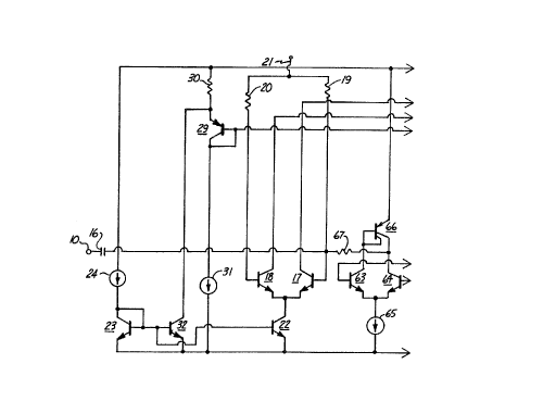
Figure 1, including Figures lA, lB and lC,
shows a circuit schematic diagram of the o~uL
amplifier embodying the present invention. A signal
input, 10, for this ouLp~L amplifier is shown to the
left in Figure lA. The ou~uL amplifier is shown in the
upper part of Figure lB as having two oùL~u~ terminals,
11 and 12, with the ouL~uL load being a center tapped
coil of a miniature loudspeaker, or receiver, 13.
2~ s 7
-4-
Loudspeaker 13 is shown having a permeable
core magnetically coupling the two halves of the center
tapped coil of that speaker to one another. The center
tap of that coil is connected to terminal, 14, intended
for connection to a source of positive voltage typically
supplied from a battery, not shown, when the amplifier
is used as part of the hearing aid. Such a battery will
typically supply an output voltage over its life in a
range of from 1.05 to 1.55 V. The other side of such a
voltage source is intended for connection to a yLv~lld
reference terminal, 15. The left-hand coil half of the
center tapped coil in loudspeaker 13 is connected
between positive voltage supply terminal 14 and
amplifier output 11, and the right-hand half is
connected between tel inAl 14 and amplifier output 12.
Signals to be amplified to operate loudspeaker
13 are provided to input 10 of the amplifier of Figure
1, and from there are coupled through a capacitor, 16,
which decouples the voltage levels about which such a
signal is supplied by the source thereof from the
voltage levels about which the input circuitry of the
ampli~ier of Figure 1 operates. Capacitor 16 is the
only capacitor which must be supplied externally for the
entirety of the amplifier shown in Figure 1 due to the
need of a capacitance value in e~cess of that which can
be conveniently supplied as part of the monolithic
integrated circuit chip in which the remaining parts of
the output amplifier circuitry of Figure 1 are typically
provided. This need for only a single capacitor in the
output amplifier circuit of Figure 1 is distinguished
from the more typical use of at least two additional
capacitors to decouple normal ~oltage operating levels
at the output of the amplifier from those at the input
2C?~
--5--
of the amplifier. This is done because of the usual
need for feedback connections between the amplifier
output and input to control system gain and to control
the output impedance characteristics which arise from
the use of an output loudspeaker such as loudspeaker 13.
Such loudspeakers have electrical
characteristics which depend not only on the electrical
materials present, but also on the ?ch~nical
construction of the load device and the acoustical
surroundings in which such a device is placed. That is,
the electrical impedance characteristic of the
loudspeaker 13 will reflect therein ?~h~nical
structural resonances modified by, and perhaps added to
by, resonances arising as a result of the acoustical
impedance faced by loudspeaker 13. The occurrence of
such resonances leads to uneven perfo~ ~nce across the
frequency range in which the system is to operate.
Improvements in these r~son~nce characteristics to
reduce performance differences between different parts
of the operating frequency spectrum of the system are
usually obtained through the use of negative feedback
from the amplifier ou~ to some point earlier along
the amplifier signal path.
The signals supplied at input 10 of the
amplifier in Figure lA, coupled through capacitor 16,
are applied to the base of an input differential
amplifier having a pair of matched npn bipolar
transistors, 17 and 18. Capacitor 16 has the side
thereof opposite the one connected to input 10 connected
to the base of transistor 17. Also connected to the
base of transistor 17 is a bias resistor, 19. A bias
resistor, 20, of similar value is correspondingly
connected to the base of transistor 18. The other sides
--6--
of bias resistors 19 and 20 are each connected to a
terminal means, 21, adapted for connection to a well
regulated supply of positive voltage. The value of this
regulated positive voltage is typically chosen to be
0.925 V for the battery voltage values given above, and
the source of that voltage is the positive voltage
supply source connected to terminal 14 which is also
connected to a voltage regulator circuit, not shown.
The output of that voltage regulator circuit is then
supplied to teL ; n~l 21.
The emitters of the input differential bipolar
transistors 17 and 18 in Figure lA are connected to the
collector of a further npn bipolar transistor, 22,
having its emitter connected to ground reference
terminal 15. The current drawn at the collector of
transistor 22 is held at a care~ully fixed, though
selectable, value so that the input differential
amplifier based on matched bipolar transistors 17 and 18
converts "single-ended" signals from input 10, those
being signals typically provided there with respect to
ground reference terminal 15, to differential signals at
the collectors of those transistors.
The value of the current drawn through the
collector of transistor 22 is set by a biasing
arrangement therefor including a further npn bipolar
transistor, 23, which is well matched to bipolar
transistor 22 with the exception of having the collector
area thereof being just twice that o~ transistor 23.
Since the emitter of transistor 23 is also connected to
ground reference terminal 15, and since the bases of
transistors 22 and 23 are directly connected to one
another-so that the same voltage occurs across the base-
to-emitter junction of each, this arrangement assures
;2r~ 7
that the current drawn at the collector of transistor 22
will be just twice that drawn at the collector of
transistor 23. The values of those currents are set by
à current source, 24, having the current draw terminal
thereof connected to terminal 14 and the current supply
terminal thereof connected to the collector of
transistor 23 and the bases of transistors 22 and 23.
The collector of transistor 23 will draw all the current
supplied by current source 24 beyond that required for
the base thereof and the bases of the other transistors
connected thereto which will be negligible if such
transistors have high current gains. As a result, the
collector of transistor 22 will essentially draw twice
the current value supplied by current source 24. If
transistors 17 and 18 are well matched, they will each
draw approximately the same collector current in the
absence of a signal at input 10 of the amplifier, and so
the collectors of transistors 17 and 18 will each draw
a current in this circumstance essentially equal to that
supplied by current source 24.
The collectors of transistors 17 and 18 are
each connected to the inputs of a corresponding one of
a pair of current controlled current generatin~ means,
or controllers, shown in Figure lB and used to operate
the output devices connected to the output amplifier
ou~ s 11 and 12. Transistor 17 has its collector
connected to the emitter of a pnp bipolar transistor,
25, and the collector of transistor 18 is connected to
the emitter of another pnp bipolar transistor, 26. Also
connected between positive voltage te, in~l 14 and t~e
emitter of transistor 25 is a current level setting
resistor, 27, and similarly, a current level setting
2~ 7
--8
resistor, 28, is connected between terminal 14 and the
emitter of transistor 26.
Pnp bipolar transistor 25 and current level
setting resistor 27 together form one of the output
portions of a simple current mirror arrangement which is
used to provide a current of a selected value at the
collector of transistor 25 in the absence of an input
signal at input terminal 10. This current mirror
arrangement is, however, modified to alter such a
current so supplied from that value which would occur as
a result of it being set by the current mirror
arrangement alone to values instead reflecting other
input signals which are provided to this current mirror
arrangement output portion. Similarly, pnp bipolar
transistor 26 and current level setting resistor 28 are
also another output portion of this current mirror
arrangement for providing a selected current at the
collector of transistor 26 in the absence of an input
signal at input 10, but again this current mirror o~uL
portion is modified so that the current output therefrom
will also reflect other input signals provided thereto.
The control portion of this current mirror
arrangement which primarily sets the output portions'
currents in the absence of an input signal at input 10
comprises a further pnp bipolar transistor, 29, and its
: current level setting resistor, 30, shown in the upper
portion of Figure lA. Resistor 30 is connected between
positive voltage te~ i n~ 1 14 and the emitter of
transistor 29. The base of pnp bipolar transistor 29 is
connected to its collector and to the bases of pnp
bipolar transistors 25 and 26. A current source, 31,
has its current draw te- ;n~l connected to the base and
_9_
collector of transistor 29 and its current supply
terminal connected to ground reference terminal 15.
Current source 31 draws a selected current
from the collector and base of transistor 29 with the
proportion drawn from each depending on its current
gain. Transistor 29 and transistors 25 and 26 are well
matched to one another and formed as lateral pnp bipolar
transistors in the monolithic integrated circuit
containing the circuitry for the ou~ amplifier.
Since the values of resistors 27 and 28 are equal to one
another and to the value of resistor 30, the current
drawn by current source 31 from transistor 29 will
essentially match the total of the current supplied
through the collectors and bases of each of transistors
25 and 26. However, because transistors 25, 26 and 29
are all lateral bipolar pnp transistors, the gains
thereof often will be relatively low, and so the base
currents drawn through each of these transistors will
often not be negligible. Thus, the current supplied at
the collectors of transistors 25 and 26 will often be
significantly less than the current drawn by current
source 31. On the other hand, since transistors in this
current mirror arrangement are well matched, as are the
current level setting resistors, the collector currents
of transistors 25, 26 and 29 will be substantially equal
insofar as they are set by the current mirror col,~,ol
portion circuitry involving transistor 29, resistor 30
and current source 31.
Of course, one of the other sources of signals
operating the current mirror arrangement output portions
in addition to the primary control portion of the
current mirror arrangement circuit are the collector
currents from transistors 17 and 18. Since these
2~?6~ y q7
--10--
currents are substantially drawn through corresponding
current level setting resistors 27 and 28, increases
therein increase the voltage drops across those
resistors and will lead to decreases in the collector
currents of transistors 25 and 26 because of the
relatively constant setting of the base voltages of
those transistors by current level setting resistor 30
and the emitter-to-base voltage of transistor 29.
Conditions in the current mirror output portions due-to
the drawing of such collector currents therein by the
collectors of transistors 17 and 18 in the absence of an
input signal at input 10 are kept similar to conditions
in the primary control portion of this current mirror
arrangement by drawing a similar current at the emitter
of transistor 29 through a further npn bipolar
transistor, 32. Npn bipolar transistor 32 is well
matched with npn bipolar transistor 23, and has both its
emitter and its base directly connected to those of
transistor 23. As a result, the current drawn in the
collector of transistor 32 is essentially equal to that
supplied by current source 24. This current is drawn
through resistor 30 as are similar currents from the
collectors of transistors 17 and 18 drawn through
resistors 27 and 28 in the absence of an amplifier input
signal. Hence, in the absence of an input signal at
input 10, voltage and current conditions at the emitters
of transistors 25 and 26 are essentially the same as
those at the emitter of transistor 29.
The provision of an input signal at input 10
of the output amplifier, however, causes differentials
in the currents drawn at the collectors of transistors
17 and 18 which are superimposed upon the currents drawn
there in the a~sence of an input signal at input 10.
~r~ 7
Thus, a positive signal at input 10 coupled through
capacitor 16 to the base of transistor 17 will lead to
an increased current drawn at the collector of
transistor 17 substantially through resistor 27, and a
decreased current drawn at the collector of transistor
18 drawn substantially through resistor 28. An opposite
polarity signal at input 10 coupled through capacitor 16
to the base of transistor 17 will have the opposite
result in the currents drawn through resistors 27 and
28.
Because the current controlled current
generators are part of negative feedback loops, such
differential signals occurring at the inputs thereof,
the emitters of transistors 25 and 26, will be very
nearly cancelled out by feedback signals supplied from
outputs 11 and 12 of the ~uL~u~ amplifier, respectively.
Output signals at amplifier ou~u~ 11 are applied to one
end of a first feedback resistance, 33, shown in Figure
lB, and output signals developed at ouL~u~ 12 of the
output ampli~ier are applied to one end of the opposite
side first feedback resistance, 34. The signals at
output 11 applied to one end of resistor 33 are
conducted therethrough and through a second feedback
resistance, 35, which is connected in series with
resistance 33 between it and the emitter of transistor
25 to which resistance 35 is also connected. Similarly,
the ou~u~ signals applied at output 12 to an end of
resistor 34 are conducted through a second feedback
resistance, 36, which is connected in series with
resistance 34 by being provided between it and to the
emitter of transistor 26 to which resistance 36 is also
connected.
Y7
The difference between the change in the
current drawn at the collector of transistor 17 because
of a signal change at input 10 and the corresponding
change in current fed back through resistors 33 and 35
will be drawn through the input of the current
controlled generator on the left side of Figure lB, i.e.
through the emitter of transistor 25, and will pass out
the collector of that transistor. In the same ~nn~r,
the difference between the acc~ -nying current change
drawn by the collector of transistor 18 and that
corresponding current change supplied through resistors
34 and 36 will be drawn at the input of the current
controlled generator on the right-hand side of the
amplifier in Figure lB, that is, through the emitter of
corresponding transistor 26, and out the collector
thereof. Outputs 11 and 12 will ~e forced to voltage
values sufficient to make these differences very small
because of the substantial transimpedance values between
these outputs and the current controlled current
generator inputs. Thus, the gain characteristics of the
ouL~u~ amplifier past the o~ Ls of the input
differential amplifier, at least at lower frequencies,
are set primarily by resistors 33, 34, 35 and 36,
although resistors 27 and 28 have some effect, and a
further resistor has a significant effect as will be
described below (as does a current feedback circuit also
to be described below).
The differential increments and decrements in
current at the collectors of pnp bipolar transistors 25
and 26 in response to a signal at input 10 of the ou~u~
amplifier are applied to the remaining portions of the
current controlled current generators. Current changes
at the collector of transistor 25 are applied to the
~r~ 7
-13-
base of an npn ~ipolar transistor, 37, and corresponding
changes in the current at the collector of transistor 26
are applied to the base of another npn bipolar
transistor, 38, both shown in Figure lB. The emitters
of transistors 37 and 38 are connected to ground
reference te- ;n~l 15. The collector of transistor 37
is connected to the base of a pnp bipolar transistor,
39, and also to one of its two collectors. Similarly,
the collector of transistor 38 is connected to the base
of another pnp bipolar transistor, 40, and to one of its
two collectors.
Transistors 39 and 40 are formed as lateral
pnp transistors in the monolithic integrated circuit
chip for the output amplifier. Each of these pnp
transistors has a relatively large total collector area.
The first collector of each of these transistors that is
connected to its base has an area on the order of the
collector area of the npn bipolar transistor also
connected thereto, but the cecon~ and s -i n ing
collector of each has an area seven times that of the
first collector thereof.
Since transistor 39 has its emitter connected
to positive reference voltage te~ in~l 14, it is in
series with transistor 37 between positive voltage
te- in~l 14 and ground reference teL in~l 15, as is the
similar series combination of pnp transistor 40, also
having its emitter connected to terminal 14, and npn
transistor 38. The choice of a pnp transistor for each
of transistors 39 and 40 in these arrangements rather
than npn transistors allows the circuit to operate at
lower voltages between terminals 14 and 15. This is
important as a battery connPcted between those terminals
begins to come toward the end of its life with its
output voltage falling.
The result of these series arrangements is
that, rather than two base-to-emitter voltage drops
being required between terminals 14 and 15 which would
be the situation if the collectors of transistors 37 and
38 were each connected to the base of another
corresponding npn transistor, there is only one such
base-to-emitter voltage drop between these teL in~l~ for
each of npn transistors 37 and 38 plus the collector-
emitter saturation voltage of the corresponding pnp
transistor which is several tenths of a volt less than
a base-to-emitter voltage drop. The relatively large
collector areas taken by pnp bipolar transistors 39 and
aid in making the saturation voltage thereof
relatively small. Similar series relationships between
terminals 14 and 15, providing a ;n; o~ a saturation
voltage in series with a base-to-emitter voltage, occurs
between transistors 25 and 37, and between transistors
26 and 38.
The second collector of transistor 39 is
connected to the base of an ou~uL npn bipolar
transistor, 41, and the second collector of transistor
40 is also connected to the base of another output npn
bipolar transistor, 42. Since transistors 41 and 42 are
output devices, they are also relatively large collector
area transistors each having a collector area sixteen
times that of the collector areas of transistors 37 and
38. As transistors 41 and 42 must be capable of
conducting currents therethrough of up to 40 mA, the
large collector areas of pnp bipolar transistors 39 and
are also advantageous in the event that the
monolithic integrated circuit fabrication process
-15- ~r~ 7
happens to yield relatively low current gains for
transistors 41 and 42~ In that situation, substantial
currents must be supplied to the second collectors of
transistors 39 and 40 to force transistors 41 and 42 to
conduct such a large collector current in each.
Through having the first collector of each of
transistors 39 and 40 connected to its base, the ~i
current gain of these transistors is fixed at seven.
This arrangement is used to aid in the providing of a
stable amplifier. Too high a gain in the left-hand
current controlled current generator cascade of
transistors 37, 39 and 41 and in the right-hand
generator cascade of transistors 38, 40 and 42 leads to
feedba~k loop stability problems. Limiting the gain of
the pnp transistors is an e~sier way to stabilize the
loop as compared to providing a complicated compensation
network for that loop. Further, too large a gain in the
pnp transistors in these cascades, if coupled with large
gains in the output npn transistors therein, leads to
very small currents in the initial npn transistors in
these cascades, transistors 37 and 38. Such very small
currents therethrough make transistors 37 and 38
relatively slow which can also lead to feedback loop
stability problems.
The current gains of these cascades will, of
course, at sufficiently high currents be limited by
saturation effects or by the ~i ;nish;ng of the current
gain o~ the transistors at higher currents. At currents
below the onset of such effects, these transistor
cascades each exhibit very high current gains on the
order of the current gains of each of the two npn
transistors therein multiplied together and that result
~r~ 4~7
-16-
then multiplied by the current gain of the cascade pnp
transistor, or seven.
The second collectors of each of pnp
transistors 39 and 40 are also connected to one another
through a string of series resistors as shown in Figure
lB. Thus, there is a first resistor, 43, on the left
side of Figure lB in this string connected directly to
the second collector of transistor 39. A similar
resistor, 44, is the first resistor in this string. on
the other side of that figure and is connected to the
second collector of transistor 40. A second resistor,
45, in the resistor string on the left side of the
figure is connected to a second resistor, 46, in the
string on the right side of the figure, and these last
two resistors are connected directly between resistors
43 and 44. ~ typical value for each of these resistors
is 48 kn.
The junction of resistors 45 and 46 also has
the bases of two further transistors connected thereto,
each closing an inner feedback loop in the corresponding
current controlled current generator on either side of
Figure lB. Thus, a further npn bipolar transistor, 47,
has its base connected to the junction of resistors 45
and 46, and its emitter connected to ground reference
te, ;n~l 15. The collector of transistor 47 is
connected to the base of transistor 37 to thereby close
the inner feedback loop in the current controlled
current generator on the left of that figure.
Similarly, a further npn bipolar transistor, 48, has its
base connected to the junction of resistors 45 and 46,
and its emitter connected to ground reference terminal
15. Again, the inner feedback loop in the current
controlled generator on the opposite side of the figure
-17-
is closed by having the collector of transistor 48
connected to the base of transistor 38.
The closing of these two inner feedback loops
thereby forms the two current controlled current
generators, one on either side of t~e ouL~u~ amplifier
portion shown in Figure lB. Thus, for the left side
inner feedback loop, current supplied by the collector
of transistor 25 is applied to the base of transistor
37, and a corresponding current is drawn through -the
base of transistor 39 by the collector of transistor 37.
That current through the base of transistor 39 causes a
current to flow through its second collector, which also
flows through resistors 43 and 45, and partly into the
base of transistor 47. This last current flow will be
just enough to cause the collector of transistor 47 to
draw almost all of the current supplied by the collector
of transistor 25 as the high gain of this inner loop
means only a slight current needs to be supplied to the
base of transistor 37.
Some of the current supplied by the second
collector of transistor 39 in this left side inner loop,
in passing through resistors 43 and 45, also passes
through a further npn bipolar transistor, 49.
Transistor 49 has its base and collector connected to
the junction of transistors 45 and 46, and its emitter
connected to ground reference te- in~l 15 to thus be
diode-connected therebetween. The current drawn at the
collector of transistor 47 must be essentially that
drawn at the collector of transistor 25 because of the
high current gain in the loop formed by transistors 37,
41 and 47. Thus, an increment in current at the
collector of transistor 25 will lead to a similar
in~L~ ?nt of current passing through the second
-18-
collector of transistor 39, and through resistors 43 and
45 to ground through transistor 49.
Similarly, a change in current at the
collector of transistor 26 is applied to the base of
transistor 38 so that its collector draws a
corresponding current from the base of pnp transistor
40. That current will be sufficient so that the current
from its second collector, flowing through resistors 44
and 46 and then through transistor 49 and the base-of
transistor 48, will yield very nearly the same current
being drawn at the collector of transistor 48 as was
supplied from the collector of transistor 26 because of
the high current gain around the loop formed by
transistors 38, 40 and 48. Thus, this change in current
at the collector of transistor 26 will be reflected in
the change in current provided at the second collector
of transistor 40. The pressnce of transistor 49
requires that half of the n~ inAl current flowing in the
collectors of transistors 25 and 26 will flow in series
resistor combination 43 and 45 and in series resistor
combination 44 and 46, respectively.
As can be seen, each of these current
controlled current generators has an output impe~nce
which drives the corresponding one of the npn ouL~uL
transistors 41 and 40, the emitters of which are
connected to ground reference terminal 15. The one of
these output impedances associated with the current
controlled current generator on the left side of Figure
lB includes resistors 43 and 45, and diode-connected
transistor 49. On the right-hand side of that figure,
the current controlled current generator there has an
out~uL impedance involving resistors 44 and 46 and
diode-connected transistor 49. Hence, the output
2~ 7
impedances of these two current controlled generators
share a common circuit component, diode-connected
transistor 49.
The change in current in the second collector
of transistor 39, applied through the output impedance
of the left side current controlled current generator,
controls the current drawn at the collector of ou~pu~
npn transistor 41 since the base and emitter thereof are
connected across the output impedance of that generator.
Similarly, the base and emitter of npn ou~ transistor
42 are connected across the ou~uL impe~nce of the
right side current controlled current generator, and so
current changes at the second collector of transistor 40
control the current drawn at the collector of transistor
42. The collector of transistor 41 is connected to
output terminal 11 of the amplifier, and the collector
of ou~pu~ transistor 42 is conne~ted to o~u~ terminal
12 of the amplifier.
Feedback resistor 35 and feedback resistor 36,
will each provide signal currents therethrough to the
inputs of the corresponding current controlled current
generator which very nearly cancel the signal currents
drawn because of input signals on amplifier input 10 at
the corresponding ou~ s of the input differential
amplifier, the collectors of transistors 17 and 18, due
to the negative feedback involved. Thus, the (a)
remaining relatively steady currents flowing at the
emitters of transistors 25 and 26, and so at the
collectors thereof, as set by resistors 27 and 28 and by
the steady currents drawn at the collectors of
transistors 17 and 18 in the absence of signals at input
10, and the (b) steady currents drawn at the bases of
transistors 25 and 26 due to current source 31, will
-20-
together set the quiescent current flows in the
collectors of output transistors 41 and 42. As
described above, such current flows at the collectors of
transistors 25 and 26 also flow in the second collectors
of transistors 39 and 40. Since transistor 41 is well
matched to transistors 47 and 49, with the exception of
collector areas, the base current flowing through
transistor 41 will be the base currents flowing in those
two transistors plus an additional in~l~ ?nt due to the
higher base voltage on the base thereof because of the
voltage drops across resistors 43 and 45. If the
voltage drops that occur across these resistors are not
large, the current drawn through transistor 41 in the
absence of a signal at input 10 of the ouL~uL amplifier
would be approximately sixteen times that flowing in the
collectors of transistors 47 and 49 because of the
collector area of transistor 41 being sixteen times that
of those transistors. A similar relation~hip occurs
between transistor 42 and transistors 48 and 49 to set
the quiescent current through transistor 42 for a
similar assumption concerning the voltage drops across
resistors 44 and 46.
The presence of transistor 49 incxeases the
current drawn through resistors 43 and 45 on the left
side of the amplifier portion shown in Figure lB and
through resistors 44 and -46 on the right side of that
amplifier portion, which increases the quiescent
collector current through o~ L transistors 41 and 42
as compared to the values that would flow therethrough
3~ otherwise which, as stated above, would be around
sixteen times that flowing in the collectors of
transistors 47 and 48, respectively. Thus, changing the
values of the currents at the collectors of transistors
~r ~ 7
-21-
25 and 26 to change the quiescent currents in ou~u~
transistors 41 and 42 will do so, though not only
because of a corresponding change in current at the
second collector of transistors 39 and 40. Rather, in
addition, the voltage drop across the corresponding
current controlled current generator output impedance
resistors in parallel with these ou~ transistor base-
to-emitter junctions will be added to the base-to-
emitter voltage drop of transistor 49 across these
output transistor junction~ leading to an increased
voltage drop thereacross applied against the exponential
characteristic of such junctions to result in a
significantly greater base current in each ou~u~
transistor base.
Thus, a change in the collector current of
transistor 47 because of a change in the collector
current of transistor 25 comes about because of a very
small voltage change across the base-to-emitter junction
of transistor 47. A much larger voltage change across
the base-to-emitter junction of transistor 41 will
accompany that change across that junction of transistor
47 leading to a much larger change in quiescent current
through transistor 41. Thus, a change in current at the
collector of transistor 25 will yield a much larger
change in the quiescent current through the collector of
transistor 41.
This relationship means that a relatively
small change is required in the voltage drop across
resistor 27 in the emitter circuit of transistor 25 to
cause a significant change in the quiescent current
flowing through transistor 41. This result is
important, since resistor 27 has to be fairly sizable if
signals at input 10 of the operational amplifier
. .
~r ~ 7
affecting the collector currents of transistors 17 and
18 are to provide significant signals at the emitter of
transistor 25 serving as the right current controlled
current generator input based on these input signals.
Yet, the voltage drop across resistor 27, to set the
quiescent collector current flow through transistor 41,
cannot be permitted to be very largs if this ouL~L
amplifier is to be usable with a relatively low value of
supply voltage provided between voltage supply terminal
14 and ground reference terminal 15 as is nec~ss~ry, for
instance, in using a hearing aid battery for this
purpose. Thus, resistor 27 has to be fairly large to
permit good signal amplification, and yet must be in a
circuit arrangement which allows a large adjustment of
quiescent current value for different kinds of
loudspeakers 13 without the oc~uL~ence of a large
voltage drop thereacross. Hence, the exponential-like
relationship between the quiescent collector current
flow of output transistor 41 and the voltage drop across
resistor 27 is a significant characteristic of this
output amplifier. A similar relationship occurs between
the voltage drop across resistor 28 and the quiescent
current flow through the collector of output transistor
42.
Since ouL~L transistors 41 and 42 operate
between the coil halves of loudspeaker 13, each
connected to positive voltage terminal 14 on one side
thereof and ground reference 15 on the other side, a
signal current increase on one side of the ou~
amplifier psrtion shown in Figure lB at either of
amplifier ouL~uLs 11 or 12 cannot be balanced in the
sense of supplying a similar current in the opposite
direction through the other output. That is, each of
;~(?$~ 7
output transistors 41 and 42 can either draw a current
through its corresponding half of the loudspeaker 13
load in the "on" condition or go into the "off"
condition - no significant current can be supplied by
the opposite output transistor through the opposite side
of the load if the first output transistor is on. The
collectors of transistors 41 and 42 can operate between
a positive voltage value and the ground voltage value as
sinks of current through loudspeaker 13 coil halves, but
they cannot become sources of current therethrough.
Hence, nearly always, either transistor 41 or 42 is in
the "off" condition while the other is in the "on"
condition.
Yet, even in these circumstances, the bases of
these output transistors must change both above and
below a voltage value balance point if there is to be
any output signal applied across any part of the ~u~u-
load formed by the coil of loudspeaker 13. That is,
when one of the ou~uL transistors is in the "off"
condition, the base voltage thereof must be the negative
of the base voltage of the "on" condition transistor
with respect to this voltage value balance point. In
the absence of such a balanced change at the bases of
one of transistors 41 and 42 by having the voltage at
the base of one going above such a voltage value point
while that of the other correspondingly goes below, the
signals supplied to such bases would appear as a common
mode signal which would be eliminated by the feedback in
the current controlled current generators leaving no
signal across the ouL~u~ load coil.
Thus, an increase in the current at the
collector of transistor 25 ~ust be accompanied by a
decrease in the current at the collector of transistor
2~'~5~ ~7
26, i.e. operate differentially, if there is to be a
resultant signal across load coil of loudspeaker 13.
Otherwise, an increase in collector current for
transistor 25, leading to an increase in current at the
second collector of transistor 39, would not only tend
to increase the current at the base of transistor 41,
but would also tend to increase the current at the base
of transistor 42 through resistors 43, 45, 46 and 44.
The resulting increase in voltage at the junction of
resistors 45 and 46 would be sensed by the bases of
transistors 47 and 48 and, as a result, be cancelled out
jointly by each of them to thus eliminate any
significant change in the collector currents of output
transistors 41 and 42. This would result in no
substantial signal across any part of the ouL~uL load
coil of loudspeaker 13.
If, however, the voltage at the junction of
resistors 45 and 46 stays constant through any change in
voltage across resistors 43 and 45 being balanced by a
corresponding opposite change in voltage across
resistors 44 and 46, there will be no change in voltage
at the junction of resistors 45 and 46 to be sensed by
either of transistors 47 or 48. As a result, one of
output transistors 41 and 42 would have the collector
current therethrou~h increased and the r ~ ~ i n; n~ one of
these output transistors would be forced towards the
"off" condition.
Such a differential signal result at the bases
of ou~uL transistors 41 and 42 is supplied, of course,
by the differential ouL~L signals o~ the input
differential amplifier based on transistors 17 and 18 in
response to input signals at amplifier input 10. This
is the only source of this result for load halves
2~?5~ 7
-25-
between positive voltage terminal 14 and amplifier
outputs 11 and 12 which do not directly interact with
one another, such as for resistive loads being provided
between positive voltage terminal 14 and amplifier
outputs 11 and 12. For load halves which are directly
interactive, such as the coil halves in loudspeaker 13
formed on a common permeable material core, the
interactive coupling will also enter into the
differential action for the coil winding directions
shown in Figure lB, and will result in the output
voltage at times rising above that supplied at te, ;n~l
14. A further aid in this regard is the current
feedback circuitry provided in this ou~L amplifier
which is shown primarily in Figure lC and will be
described below.
This need for having voltage on the base of
one of output transistors 41 and 42 change in value in
the opposite direction from that of the other about the
voltage value at the junction of resistors 45 and 46
requires choosing in effect a sufficient quiescent
collector current through output transistors 41 and 42.
That is, a sufficient current flow through the current
controlled current generator ~uL~uL ; ~ nce resistors
43 and 45 on the left side of the amplifier portion in
Figure lB and the current controlled current generator
output impedance resistors 44 and 46 on the opposite
side is needed so that such changes about the voltage at
the junction of resistors 45 and 46 can be accommodated.
The lower the load i e~nce, the higher the
output transistor quiescent currents must be since the
currents flowing through resistors 43 and 45 and through
resistors 44 and 46, which s~t these output transistor
quiescent currents, must also be greater to provide a
'7
sufficient range of voltage values for such changes in
the voltages at the bases of the output transistors 41
and 42 without clipping occurring. The lower the
impedance occurring in the load, the greater the ~uLLen~
changes therethrough must be to provide sufficient
signals to operate that load, and so greater changes are
required in the voltages at the bases of output
transistors 41 and 42.
The capability to reduce the voltage on a base
of one of the output transistors 41 and 42 below that
occurring at the junction of resistors 45 and 46 comes
about because of the selectable value currents drawn at
these bases by the current feedback circuitry of Figure
lC which is described below. The larger the curxents
drawn at the output transistor bases by the current
feedback circuitry, the greater the currents which must
be supplied through the second collectors of transistors
39 and 40 to raise the voltages sufficiently across the
series resistors 43 and 45 and across the series
resistors 44 and 46 to be able to supply the current
feedback circuitry demand. The larger voltage drop
across these series resistor combinations acc ~'~tes
the need for allowing the o~uL transistor voltages to
drop below the voltage value ~A 1 ~nce point at the
junction of resistors 45 and 46, as a reduction in the
current at either of the second collectors of
transistors 39 or 40 will not support the current demand
of the feedback circuitry resulting in a reduction of
the voltage across the corresponding series resistor
combination to being below that voltage point. This
larger voltage drop across these series resistor
combinations also increases the quiescent currents in
the output transistors.
2C~ ', 7
-27-
In the ~eedback circuitry, the current value
setting therein which increases the current drawn
thereby at the bases of the output transistors to
accommodate symmetrical voltage changes about the
voltage at the junction of resistors 45 and 46 to
thereby permit larger output current changes for smaller
impedance loads also sets the amount of current
feedback. This is possible since a reduced amount of
current feedback giving less amplifier gain attenuation
is needed in these same circumstances.
At relatively low values of amplifier gain
(which is set by the combination of choices for the
value of the current in current source 24, the value of
a current setting in the current feedback to be
described, and the values of the various feedback
resistors) and something greater than i n;
loudspeaker ; c~nces, very small quiescent currents
are all that are required. In those circumstances, the
amplifier distortion will be dominated by that occurring
in the input differential amplifier. This distortion
will be just that characteristic of two-transistor
differential amplifiers, and will be a maximum as the
input differential amplifier just goes into saturation.
For higher gains, the distortion will ~i ;n;sh as this
gain will be supplied by the r~ ~;n~er of the amplifier
past the input differential amplifier, and so this input
differential amplifier will be operated with lower
signal values therein reducing its distortion.
A further resistor, 50, is provided connected
between the junction of feedback resistors 33 and 35,
and the junction of feedback resistors 34 and 36.
Resistor 50 reduces the current required to be shifted
by the input differential amplifier based on transistors
2~ 7
-28-
17 and 18 in response to a changed input signal at
amplifier input 10 to thereby achieve a corresponding
voltage value shift at outputs 11 and 12 of the output
amplifier of a given magnitude, i.e. resistor 50
increases the gain of the amplifier. Since smaller
current shifts are required in the input differential
amplifier based on transistors 17 and 18 because of the
presence of resistor 50, a smaller quiescent current can
be used therein, as set by transistors 22 and 23 with
current source 24, and so a smaller standby current
drain for the output amplifier as a whole can be
achieved.
Thus, if the signal applied at input 10 of the
output amplifier causes an increase in the current drawn
by the collector of transistor 17, there will be a
corresponding decrease in the current drawn at the
collector of transistor 1~. As a result, there will be
a tendency toward an increase in the voltage drop across
resistor 27 and a tendency toward a decrease in the
voltage drop across resistor 28. Because of the
negative feedback connection, there will be a
corresponding increase in the voltage at output 11 of
the amplifier and a correspon~ing decrease in the
voltage at ou~uL 12 thereof t~n~ing to nullify these
changes in currents drawn at the collectors of
transistors 17 and 18.
However, the voltage at node 11 will have to
rise further, and the voltage at node 12 will have to
fall further, than it would in the absence of resistor
50 since current will be removed from the junction of
resistors 33 and 35 by resistor 50 and supplied to the
junction of resistors 34 and 36. The increase in
voltage at ou~L 11 will be re~uired to supply not only
S,11"7
-29-
the current needed to nullify the added current drawn at
the collector of transistor 17, but to also supply the
current being drawn through resistor 50 due to the
lowered voltage at output 12. Thus, a greater voltage
differential will occur between outputs 11 and 12 by the
presence of resistor 50 than would otherwise occur for
a change in differential currents at the collectors of
transistors 17 and 18 in the input differential
amplifier. HPnce, that presence provides a clear
increase in the gain of the output amplifier because of
resistor 50.
Thus, the output voltage differential between
outputs 11 and 12 in response to a differential change
in currents drawn at the collectors of transistors 17
and 18 of the input amplifier dep~n~ not only on the
values of the feedback resistors 33 through 36, and the
resistance values of the bias resistors 27 and 28, but
also on the resistance value of resistor 50. This gain,
or transimpe~ance, of the o~ L amplifier portion shown
in Figure lB can be expressed as follows as~ g
symmetrically positioned resistors have equal values:
v12-vll R~RB
In this equation, RA ~ R35 = R36, RB = R33 = R34, RC = R27
= R28~ and RD = Rso- Typical values of these
resistances are RA = RB = RD = 48 kn and RC = 8 kn (as
does resistor 30 earlier noted to have a value equal to
that of resistors 27 and 28). As can be clearly seen
from this equation, decreasing the value of resistor 50,
or RD, clearly increases the transimped~nce of the
amplifier portion shown in Figure lB. The feedback
resistor resistance values are relatively large so the
-3~-
current conducted by them in the absence of an input
signal at input 10 will be small and unimportant insofar
as the setting of the quiescent current in output
transistors 41 and 42 is concerned.
The limit on the changes in currents which can
be drawn at the collectors of transistors 17 and 18 in
the input differential amplifier determines the maximum
output possible of the output amplifier at its outputs
11 and 12 if these outputs have not reached the
saturation limits set by the voltage on te- ;nAl 14
(ignoring inductive transients). The current set by
transistors 22 and 23 in conjunction with current source
24 for this input differential amplifier determines the
~ range of current change possible at the
collectors of transistors 17 and 18. This range is
equal to a -~; value of the current drawn by
transistor 22 if one of transistors 17 and 18 draws all
of that current at its collector, and to a value of zero
if the other of those transistors draws all that current
at its collector. Thus, the maximum differential in the
current being drawn at the collectors of transistors 17
and 18 is equal ~o the current set to be drawn by
transistor 22. This current substituted in the above
eguation gives as a result the maximum voltage
differential which can be provided between ouL~Ls 11
and 12 in the absence of current feedback and in the
absence of these outputs reaching the saturation limit
provided by the voltage on teL inAl 14. This maximum
voltage differential in these circu~stances dete~ ines
the ~ m voltage which can occur across the coils of
loudspeaker 13. No greater voltage can occur since
there is no further increase possible in the current
Z~ 7
differential between the currents drawn at the
collectors of transistors 17 and 18.
As a result, the output voltage change of the
output amplifier is effectively limited to a -Y;
value set by the input differential amplifier if the
~i ]m current change of that amplifier is kept
sufficiently small to avoid having the limit be set by
output saturation effects because of the voltage
provided on terminal 14. This is accomplished without
the need to include any added component solely for the
purpose of providing such a limit for the ~i Im
excursion of that voltage. The absence of any such
excursion limiting components avoids current drains
therethrough in those situations in which the o~u~
amplifier is driven into saturation, which is likely to
happen in a hearing aid arrangement for example, as
external acoustical energy ranges will on occasion be
greater than the range of permissible inputs to keep the
amplifier within its operating range at its ou~u~.
Since there are no ol~u~ range excursion limiting
components, there is nothing added to the feedback loops
involved which could create any instability in the
operation thereof. Further, reaching the voltage change
limit is done rather gracefully compared to the use of
o~u~ excursion limiting devices and, as a result,
there is likely to be much less harsh output signal
components generated in reaching the output limits of
the o~L~uL amplifier by this method.
As noted above, there can be rather
significant changes in the ou~ impedance presented by
loudspeaker 13 over the desired operating frequency
range due to electromech~n;cal and acoustical reson~ncPs
associated with that speaker. The lower loudspeaker
-32-
impedance values which occur over some parts of the
output operating frequency range will lead to a much
greater output current being drawn at those frequencies
unless such low impedance values are counteracted in
some manner. The manner used here is to provide current
feedback in the output amplifier as the means of
compensating such low impedance values in the i~pedance
characteristic provided by loudspeaker 13 to outputs 11
and 12 of the output amplifier. Such current feedback
is provided by the circuitry shown primarily in Figure
lC.
Of course, the parts of the load i~pe~nce
characteristic over frequency exhibited by loudspeaker
13 having high impedance values would cause much greater
output voltages at outputs 11 and 12 if not
counteracted. However, this is counteracted by the use
of voltage feedback, and this voltage feedback is
supplied by the feedback resistors described above.
As previously described, the currents from the
second collectors of pnp bipolar transistors 39 and 40
supply the control currents for output npn bipolar
transistors 41 and 42 in Figure lB. Some of this
current at the second collector of transistor 39 is
carried through resistors 43 and 45, and the base and
collector of transistor 49, across which together is
provided the base-to-emitter junction of ou~u~
transistor 41. Similarly, such current from the second
collector of transistor 40 is carried through resistors
44 and 46, and through the base and collector of
transistor 49, across which together is the base-to-
emitter junction of output transistor 42. As a result,
the voltage drops at the bases of these ou~u~
transistors are a clear indicator as to the collector
' 7
-33-
currents drawn by them, and so these voltage drops are
sensed by the current feedback circuitry of Figure lC by
pairs of collector coupled npn bipolar transistors as
the basis for deter ; ni ng the magnitude of the feedback
signals to be supplied in view of the collector currents
magnitudes so sensed.
This method of sensing the output transistor
collector currents avoids placing any components in
series with the output transistors, such as resistors,
as the basis for sensing the currents therethrough as
often done and which would limit the possible ouL~u~
voltage range. Avoiding such a limitation is important
if a low output voltage value voltage source such as a
hearing aid battery is provided between positive voltage
te~ ;n~l 14 and ground reference terminal 15.
The voltage sensed at the base of out~
transistor 41 is applied to the base of an npn bipolar
transistor, 51, in the first of these sensing transistor
pairs, and the voltage at the base of output transistor
42 is applied to the base of a further npn bipolar
transistor, 52, also in the first of these sensing
pairs. Similarly, the voltage at the base of ou~uL
transistor 41 is also applied to the base of an npn
bipolar transistor, 53, in the second of these sensing
transistor pairs, and the voltage at the base of ou~u~
transistor 42 is again applied to a second npn bipolar
transistor, 54, in the second sensing transistor pair.
The voltage at the base of ou~u~ transistor 41 so
applied to the bases of transistors 51 and 53 is applied
through a resistor, 55. Similarly, the voltage at the
base of o~tput transistor 42 applied as described to the
bases of transistors 52 and 54 is applied through
another resistor, 56.
2r~ 7
The emitters of each of transistors 51 through
54 are directly connected to ground reference terminal
15. The first sensing pair of transistors has the
collectors of transistors 51 and 52 therein connected to
a two-collector pnp bipolar transistor, 57. The base of
transistor 57 is connected to the first collector
thereof and to the collector of transistor 52. The
second collector of transistor 57 is connected to the
collector of transistor 51, and to the collector of
transistor 25 to serve as the output of this first
sensing pair arrangement in the current feedback
circuit. This first sensing pair output provides or
draws a feedback current in the left side current
controlled current generator of the ouL~uL amplifier
lS portion shown in Figure lB at the collector of
transistor 25. The two collectors in each of
transistors 57 and 58 each have substantially equal
areas in the monolithic integrated circuit construction
thereof. The emitter of transistor 57 is connected to
positive reference voltage terminal 14.
The second sensing pair in the current
feedbacX circuit involving transistors 53 and 54 has the
collertors of those transistors connected to another
two-collector pnp bipolar transistor, 58. The base of
transistor 58 is connected to its first collector and to
the collector of transistor 53. The second collector of
transistor 58, serving as the output of this secon~
sensing pair arrangement, is connected to the collector
of transistor 54 and to the collector of transistor 26.
This second sensing pair ou~L provides or draws a
feedback current in the right side current controll~d
current generator of the vuLpu~ amplifier portion shown
in Figure lB at the collector of transistor 26. The
2~?~5~ ~7
-35-
emitter of transistor 58 is connected to positive
reference voltage terminal 14.
If base currents for transistors 51 through 54
are all that are drawn through resistors 55 and 56, the
currents in the collectors of those transistors, since
they are well matched to output transistors 41 and 42
except for collector areas, will match the currents
flowing in the collectors of transistors 41 and 42
though reduced by a factor of sixteen. This factor of
sixteen is due to the differing collector areas in
transistors 41 and 42 compared to those of transistors
51 through 54. If the current at the collector of
transistor 25 is increased and that at the collector of
transistor 26 is decreased due to a signal change at
input 10 of the amplifier, there will be an increase in
the current flowing in the collector of transistor 41
and an increase in the currents flowing in the
collectors of transistors 51 and 53. There will be a
corresponding decrease in the current in the collector
of transistor 42 to very little current, and a similar
decrease in the currents in the collectors of
transistors 52 and 54 to again very little current.
As a result, the very small or negligible
current in the collector of transistor 52 will mean
little current flows in the base of transistor 57 and so
very little current will flow in the collectors thereof.
On the other hand, the current increase drawn at the
collector of transistor 51 will be supplied from the
collector of transistor 25 tPn~ing to nullify the
increase in current at that collector which started the
just described process. On the other hand, the
significant increase in current at the collector of
transistor 53 will lead to substantial currents flowing
2~ 7
in the collectors of transistor 58. Since little or a
negligible amount of current will be drawn in the
collector of transistor 54, the current in the second
collector of transistor 58 will be supplied to the base
of transistor 38 to compensate for the earlier drop in
current at the collector of transistor 26 to thereby
counteract such a drop. Current changes at the
collectors of transistors 25 and 26 in the opposite
direction will lead to the opposite results.
Hence, the current feedback circuit of Figure
lC tends to counteract current changes at the collectors
of transistors 25 and 26, and will nearly nullify them
in a situation where no significant current is drawn
through resistors 55 and 56. This will be too much
feedback in many situations resulting in too great an
attenuation of the amplifier gain or transimpe~nce, and
so the circuit in Figure lC has provisions for reducing
this level of feedback. The collector of a further npn
bipolar transistor, 59, is connected to the bases of
transistors 51 and 53 and to resistor 55. Similarly,
another npn bipolar transistor, 60, has its collector
connected to the bases of transistors 52 and 54 and to
resistor 56. The emitters of both of transistors 59 and
60 are conne~ted to ~o~nd reference terminal 15. The
~5 bases of transistors 59 and 60 are each connected to a
diode-connected bipolar transistor, 61, having its
emitter connected to ground reference terminal 15 and
its collector connected to its base. A current source,
62, is connected between positive reference voltage
terminal 14 and the collector of transistor 61 to set
the current carried therethrough.
Transistors 59 and 60 are well ~atched with
transistor 61, and so the base currents flowing in
ZC~ 7
transistors 59 and 60 will be essentially that flowing
in the base of transistor 61. In these circumstances,
the collector currents at transistors 59 and 60 will be
essentially that at transistor 61, which for transistors
with substantial current gain will be essentially the
current supplied by current source 62. Since currents
drawn at the collectors of transistors 59 and 60 must be
supplied through resistors 55 and 56, a significant
voltage drop can be caused to form thereacross so that
the voltage changes at the bases of transistors 41 and
42 will be applied to transistors 51 through 54 at lower
values on their base-to-emitter characteristics. This
will have the effect of reducing the response of the
collector currents of transistors 51 through 54 and so
reduce the level of feedback signals applied at the
collectors of transistors 25 and 26.
The current supplied by current source 62 can
thus be set to provide any level of feedback desired and
to significantly change the gain of that part of the
output amplifier shown in Figure lB. In these
circumstances, the equation given above for the
transconductance of that portion of the output amplifier
must be modified to take into account the action of the
current feedback circuit shown in Fi~ure lC to provide
an accurate characterization of the behavior of that
portion of the circuitry.
Note that the current feedback circuit of
Figure lC draws increased current ~rom the bases of
output transistors 41 and 42 as the current value of
current source 62 is increased. Thus, as indicated
above, the current setting choice in the current
feedback circuitry made by choosing the value of source
62 decreases the amplifier gain attenuation due to the
2~ 7
-38-
current feedback circuit concurrently with increasing
voltage drops across resistors 55 and 56 through drawing
greater currents from the second collectors of
transistors 39 and 40, respectively. This result, as
described above, assures that the base voltages of the
output transistors will be able to swing symmetrically
about the value of the voltage occurring at the
junctions of resistors 45 and 46 to avoid the
elimination of an output signal due to common mode
effects. The larger currents in the second collectors
of transistors 39 and 40 allow greater changes to be
made in these currents so larger voltage changes can be
made across resistors 55 and 56. Correspondingly larger
voltage charges can occur across the series combination
of resistors 43 and 45 and across series resistor
combination 44 and 46, respectively.
The two sides of the output amplifier portion
shown in Figure lB are part of a negative feedback
arrangement as explained above. In such situations,
seemingly, the voltage feedback present would assure
that the currents in the collectors of output
transistors 41 and 42 in the ~hsPnce of input signals at
output amplifier input 10 would stay substantially equal
in value. However, this feedback provision is not
always adequate to assure such current matching because
so~e kinds of ouL~u~ loads, including some kinds of
loudspeakers 13, can have very low impedances therein
with a resistive component that is on the order of only
a few ohms per side. As a result, even relatively large
current differentials between the collector currents of
04LyuL transistors 41 and 42 may lead to only negligible
voltage differences occurring at ouL~s 11 and 12 of
the output amplifier.
2~
To counter such current of fsets, an of fset
differential amplifier is provided which is shown in
Figure lA based on a pair of npn bipolar transistors, 63
and 64. The emitters of transistors 63 and 64 are
connected together and to a current source, 65, at the
current draw terminal thereof. The current supply
ter in~l of current source 65 is connected to ground
reference terminal 15. A two-collector pnp bipolar
transistor, 66, has its base and its first collector
connected together and to the collector of transistor
63, and has its second collector connected to the
collector of transistor 64. Each of the collectors of
transistor 66 has an area equal to that of the other.
The emitter of transistor of 66 is connected to positive
voltage terminal 14. A resistor, 67, connects the
collector of transistor 64 to the base of transistor 17
in the input differential amplifier as well as to side
of input capacitor 16 connected to that base.
The base of transistor 63 is connected to the
junction of the series combination of resistors 43 and
45, and the base of transistor 64 is connected to the
junction of the series combination of resistors 44 and
46 to sense the voltage difference between these two
series resistor combination junctions. The voltage
divider action of series combination resistors 43 and
45, and the voltage divider action of series combination
resistors 44 and 4Ç, provides voltage difference equal
to half the voltage difference occurring between the
bases of output transistors 41 and 42. This difference
in voltage between the bases of o~u~ transistors 41
and 42 is, as explained above, a measure of the
differential in the currents at the collectors of these
two transistors in the absence of an input signal at
~ t7
-40-
input 10 of the output amplifier. The use of the two
series resistor combinations as voltage dividers to
supply signals to the bases of transistors 63 and 64
reduces the sensitivity of the circuit by two to avoid
too much of a reaction to such imbalances by the offset
differential amplifier.
If the voltage differential between the bases
of transistors 63 and 64 leads to a voltage occurring on
the base of transistor 63 greater than that occurring on
the base of transistor 64, there will be a greater
current drawn through the collector of transistor 63 and
so through the base and first collector of transistor
66. There will be a similar increase in current
supplied at the second collector of transistor 66 part
of which will be added to the current flowing through
resistor 67 as the current drawn at the collector of
transistor 64 is correspondingly re~-lce~. A voltage
differential in the opposite direction on the bases of
transistors 63 and 64 will lead to a smaller current
being drawn from the base and first collector of
transistor 66, and so a smaller current will be supplied
at the second collector of transi~tor 66. Yet, a greater
will be current drawn at the collector of transistor 64
leading to a current being drawn through resistor 67.
The ~ magnitude of any current shifts permitted
through resistor 67 for a differential voltage occurring
between the junction of series combination resistors 43
and 45 and the junction of series combination resistors
44 and 46 will be set primarily by the value of the
current drawn by current source 65 from the emitters of
transistors 63 and 64.
Assuming that the opposite side of a source of
signals connected to input 10 of the output amplifier
has a ground reference connection, the current supplied
through resistor 67 will supply charge which will be
stored on capacitor 16 and the current drawn
therethrough will remove such charge. The resultinq
voltage changes across input capacitor 16 applied to the
base of transistor 64 will change the relationship of
the collector currents in transistors 63 and 64, and so
in transistors 17 and 18, to thereby correct i h~ ~ ~nces
in the collector currents drawn through o~ L
transistors 41 and 42.
The currents supplied to and drawn from
capacitor 16 through resistor 67 will often change
rapidly and abruptly as the two sides of the output
amplifier portion shown in Figure lB have the
corresponding output transistors thereof go from the
"off" condition to the "on" condition and bacl: again.
This rapidly and sharply changing signal can be provided
at the input of the input differential amplifier on top
of that supplied by the input signal source at input 10,
and yet not cause distortion of any significance, by
keeping the currents supplied and drawn through resistor
67 to no more than being only large enough to change the
voltage across resistor l9, or capacitor 16,
sufficiently to compensate to a satisfactory extent the
expected imbalances. Since no more than a 2 mV change
across that resistor is expected to be needed, the
~i current needed to be supplied through resistor
67 is on the order of 40 nA for the component values
chosen. This small current will be relatively
negligible in showing up in the signal to be amplified
in the output amplifier if the impe~nce of capacitor 16
and the source connected to input te~ ; n~ ~ 10 of the
output amplifier is much less than the value of the
2~
resistance of resistor 19. A typical resistance value
for resistors 19 and 20 is 48 kn for each, with
capacitor 16 having a typical capacitance value of
0.015 ~F. A typical value for resistor 67 is 100 kn,
and current source 65 typically has a value of 40 nA.
In addition, the gain of the output amplifier must not
be so high that excursions occurring in the voltages at
the bases of transistors 41 and 42 become so great that
they cause the signal supplied by the offset
differential amplifier based on transistors 63 and 64 to
be of a magnitude comparable to that of the signals
supplied at input 10 of the output amplifier. The
component values chosen for the offset circuitry are
such that current mismatches in the collectors of the
output transistors are not fully counteracted but are
corrected sufficiently that the differences in currents
drawn to the collectors of transistors 41 and 42 in the
absence of an input signal at output amplifier 10 are
kept from being too different from one another.
Because the quiescent currents flowing in
output transistors 41 and 42 are kept as small as
possible, there will as a result be large and rapid
voltage excursions which occur at the bases thereof as
the opposite sides of the amplifier portion shown in
Figure lB go from the "off" condition to the "on"
condition and back. This action, of course, is
n~c~ssAry for satisfactory, ~istortionless amplifier
operation. Stabilization measures for the ou~p~
amplifier must not inhi~it this action by having a
filtering effect on the operating signals supplied at
the bases of transistors 41 and 42 even though the use
of stabilization networks always involves the showing of
some signal activity in an amplifier. This need is met
-43-
here by using stabilization networks which establish the
dominant pole of the amplifier characteristic at its
output transistors so that the signals applied to the
bases thereof have not been undesirably changed before
being so applied. As a result of this location, the
pole in the amplifier characteristic will change with
the value of the load impedance.
In view of these considerations, a pair of
series resistance and capacitance circuit branches are
provided between the collector and base of each of
output transistors 41 and 42 to establish the dl ;nAnt
pole of the output amplifier frequency response. Thus,
a capacitance, 68, is connected to the second collector
of transistor 40, and a further capacitance, 69, is
connected to the second collector of transistor 39. A
resistance, 70, is connected between capacitance 68 and
the collector of transistor 42. Similarly, a
resistance, 71, is connected between capacitance 69 and
the collector of transistor 41. Placing these series
resistance and capacitance circuits in these locations
avoids affecting the signal paths from the inputs of the
current controlled current generators to the bases of
output transistors 41 and 42 so that the higher
frequency components in those signals reach the bases of
these transistors. Thus, the lower frequency portions
are fully supplied to the bases of transistors 41 and 42
to experience the full gain of the amplifier, and only
at frequencies above those a~ which the pole is located
is there significant attenuation of the signals applied
to the bases of transistors 41 and 42. This also
reduces "crossover" distortion. The primary pole is set
at a frequency of 3 kHz for the lowest impedance kind of
coil for loudspeaker 13 based on resistors 70 and 71
~t~ y~
having a resistance value of 15 kn, and capacitances 68
and 69 having values of 100 pF which can be easily
provided in the monolithic integrated circuit containing
most of the output amplifier circuitry.
A second pole is provided by another pair of
resistance and capacitance series circuit branches.
Thus, a capacitance, 72, is connected to the collector
of transistor 26, and a similar capacitance, 73, is
connected to the collector of transistor 25. A
resistance, 74, is connected between capacitance 72 and
the collector of output transistor 42. Another
resistance, 75, is connec~ed between capacitance 73 and
the collector of ou~pu~ transistor 41. Typical
resistance value for resistors 74 and 75 is 100 ~n, and
typical capacitance value for capacitors 72 and 73 is
33 pF, which can again be easily provided in the
monolithic integrated circuit in which most of the
output amplifier is formed.
The npn bipolar transistors used in the
circuit of Figure 1 in monolithic integrated circuit
form all have the same design construction and are
reasonably well matched to one another with the
exception of differences in collector areas thereof, as
has already been indicated. Similarly, the pnp bipolar
transistors in that circuit are all constructed in the
same manner in the monolithic integrated circuit with
the exception of the number of collectors, again as has
been indicated, and so are reasonably well matched to
one another. The resistors in the monolithic integrated
circuit are formed by ion implantation in the monolithic
integrated circuit chip, and have the junctions
therearound reverse biased. In addition, in fabricating
such a monolithic integrated circuit, a separate ground
2~5'1~7
-45-
return is desirable to use from the circuit components
which are to conduct relatively high current values to
eliminate noise problems in the ground reference
interconnections to which components conducting currents
of much lower values are connected.
Although the present invention has been
described with reference to preferred embodiments,
workers skilled in the art will recognize that changes
may be made in form and detail without departing from
the spirit and scope of the invention.