Note: Descriptions are shown in the official language in which they were submitted.
1
~k~TCAPBIdILu~'fED IaIC9~T ~dg°t°°f~~T~3
Dz~DE Ana ~soD
~~It ~r~c.~I'~ua~Axaor~
Dao~c~ou~d Of Tt~e Iaaqrentisa~n
1. F'ielc~ of the $alVextt3~n
The present invention relates to a new and
improved light emitting diode that is
encapsulated with optically absorbing material
to reduce stray light, and to a new and
improved method for encapsulating a light
emitting diode to reduce stray light.
2. Description of the Dack~und Art
In designing blood glucose monitoring
instruments, the direction of development has
been toward smaller instruments that are lower
in cost. To meet these goals, more than one
function is designed into a single component.
This approach lowers the part count, reduces the
size of the instrument and increases the
reliability.
One example of this trend is the use of a
light emitting diode (TaED) to replace the
combination of an incandescent lamp, and an
interference filter in the optical system of
blood glucose monitoring instruments. examples ,
of instruments that use an LSD as a light
MS 1660
2
source include the GLUCOMETER III manufactured
by Miles, Inc., the ACCUCHECK manufactured
by
Boehringer Mannheim Gmb~T and the GLUCOSCAN
manufactured by Lifescara, Inc. Examples of
devices using an LED in a readhead are to
be
found in United States F>atent Nos. 4,552,458:
and 4,676,653 and Europs:an Patent Application
No. 83304306.6, filed July 26, 1983. LED light
sources have also been used in other diagnostic
instruments such as the instrument disclosed
in
United States Patent No. 4,755,058. The
typical LED used as a light source in the
readhead of a blood glucose monitoring system
is the standard T-1 3/4 which can be purchased
from manufacturers such as the ES Series made
by Stanley Electric Co., Ltd. or the HLMP
Series from Hewlett-Packard.
One of the problems in using a standard
LED as a light source in a blood glucose
monitoring instrument is the stray light
emitted by the LED. In a diagnostic instrument
readhead it is preferable that the LED emission
be generally collimated toward a small sample
area. Rays emitted at wide angles are
undesirable stray light that preferably are
minimized or eliminated, since stray light
in
an optical system of a readhead instrument
manifests itself as a background signal.
At least three procedures have been used
3o in instruments to control the stray light
from
an LED. One method is to ignore the existence
of stray light. By ignoring the stray light,
MS 1660
~~~~ 3'~'~l
3
however, there can be a high level of
instrument to instrument imprecision. Due to
this imprecision, ignoring the stray light has
not been considered an ~:cceptable method.
Another method of e:ontrolling stray light
is to accept only a small solid angle of the
emission from an LED.
Such an approach is used in the instrument
described in United Stai:es Patent No.
4,676,653. This approach results in an
instrument that uses only a small portion of
the available light from the LED. This
approach also reduces the magnitude of the
available signal and can make the optical
system more susceptible to noise.
Another approach is to use a shield to
avoid the detection of the stray light. Such
an approach is illustrated in European Patent
Application No. 83304306.6. This approach does
not shield the stray light flaring in
directions other than in direct line with the
shield. Commuter simulations have been
performed that suggest 'that there is a
significant amount of this light that flares in
all directions after emission from an LED, and
for this reason, shielding is not preferred.
SUMP~A3~Y Df TAE ~ielil'EN'fI~N
Briefly, the present invention is directed
to a new and improved light emitting diode used
in an instrument readhead such as in a blood
glucose monitoring instrument. The LED may be
of the standard type such as a T-1 3/4 plastic
MS 1660
~~~J..~..
LED lamp that includes a base with anode and
cathode leads extending from the base to a
location above the base. An active light
emitting element is encapsulated within an
epoxy envelope that is ~~ecurad on the base.
The epoxy envelope includes a conical side
portion and a spherical dome portion or lens
that extends above the ~;ide portion and
encloses the envelope.
l0 To reduce the amount of stray light
emitted by the active light emitting element,
the side portion and part of the spherical
dome
portion are encapsulated by optically absorbing
material. This material is placed in direct
contact with 'the envelope leaving an exposed
portion of the spherical dome portion.
Preferably, this encapsulation of the envelope
is done such that the diameter of the exposed
portion is equal to 2r[sin(x + arcsin (r/s/n))]
wherein r is the radius of the spherical dome
portion, x < arcsin (1/n) is the maximum angle
between a surface normal and a ray emitted
from
the active light emitting element that strikes
the envelope at the edge of the exposed portion
of the spherical dame, s is the distance
between the active light emitting element
and
'the center of the spherical dome portion,
and n
is the index of refraction of the epoxy
material that defines the envelope.
MS 1660
5
BRIEF' DESCRIPTION OF THE DRh,NINC~S
Other objects and advantages of the
present invention will become apparent upon
reading the following detailed description and
upon reference to the drawings in which:
FIG. 1 is a schematic illustration of a
light emitting diode and the paths of different
classes of rays of light;
FIG. 2 as a schematic illustration of a
light emitting diode similar to FIG. 1
including optically absorbing material
encapsulating the light emitting diode and
illustrating the path of the different classes
of rays of light.
FIG. 3 is a schematic illustration similar
to FIG. 2 illustrating different dimensions of
the light emitting diode; and
FIG. 4 is a schematic illustration of the
dimensions of different portions of the epoxy
envelope of the light emitting diode of the
present invention and the path and angles of
light rays used to calculate the exposed ,
portion of the envelope uncovered by the
optically absorbing material.
DESCRIPTION 0F' THE PREFERRED EI~BODIIriENT
Referring initially to FIG.1, there is
illustrated a standard T-1 3/4 plastic LED lamp
generally designated by the reference numeral
10. Only the elements of the LED 10 that are
necessary for an understanding of the present
invention will be described.
1~S 1660
6
The LED 10 includes a reflector dish 12
coined orito a cathode past 14. The cathode
post 14 is part of a cathode lead 16 extending
downwardly from the LED 10. The LED 10 also
includes an anode post 18 that extends from the
LED 10 'to an anode lead 20.
The LED 10 includes an LED chip or active
light emitting element 22 electrically
connected t~ the reflector dish 12 and the
anode post 18. The active light emitting
element 22 is positioned above a base 24 of 'the
LED 10 and is encapsulated in or covered by an
epoxy resin envelope generally designated by
the reference numeral 26. The epoxy envelope
26 includes a tapered or conical side portion
28 and an upper spherical dome portion 30. The
base 24 encloses the lower end of the epoxy
envelope 26, and the spherical dome portion 30
encloses the upper end of the epoxy envelope
26. In addition, the upper spherical dome
portion 30 functians as a magnifying lens for
the rays of light emitted from the active light
emitting element 22. Although a T-1 3/4 LED
lamp is illustrated and disclosed, it is
intended to be recognized that other LEDs with
other shaped domes, for example, a parabolic
surface of revolution, are included in this
invention as long as the diameter d of the
shape limits the angle x to less than arcsin
(1/n) .
As best illustrated in FIG. 1, the light
rays emanate from the active light emitting
MS 1660
7
element 22, strike 'the various optical
surfaces, and are refracted by 'the epoxy resin
envelope 26. A computer simulation for an LED
without a reflecting cone was used to determine
that the rays emitted from the active light
emitting element 22 can be grouped into four
classes. Class 1 rays are refracted by the
spherical dome portion 30 of the epoxy resin
envelope 26. Class 1 rays make up about 29% of
the total rays, and are the most useful rays in
an instrument readhead application since they
remain generally collimated at some distance
from the LED 10. Class 2 rays are
refracted by the spherical dome portion 30 of
the epoxy resin envelope 26 after first being
internally reflected by the side portion 28 of
the epoxy resin envelope 26. Class 2 rays make
up about 19% of the total rays. Class 2 rays
are not useful in an instrument.readhead
application as they form a ring which diverges
widely upon leaving the LED 10.
Class 3 rays pass through and are
refracted by the side portion 28 of the epoxy
resin envelope 26. Class 3 rays make up about
28% of the total rays, and are not useful as
they also form a wide diverging background upon
leaving the LED 10.
Class 4 rays are internally reflected by
the epoxy resin envelope 26 and make up the
remaining 24% of the total number of rays. As
with class 2 and 3 rays, class 4 rays are not
MS 1660
~~~_-~~N~fl
~'~~~,~~~
8
useful in an instrument readhead application
since they exit the back of the LED 10.
In order to maximize the effectiveness of
an LED 10 in an instrument readhead, it is
desirable to prevent the class 2, class 3
and
class 4 rays from exiting the LED 10. In the
present invention, this is accomplished by
encapsulating the LED 1o with an encapsulating
material 32 (FIGS.2-4). The encapsulating
material 32 is preferably an optically
absorbing material of a low reflectivity such
as black plastic or black painted material
and
can be a sleeve that is slipped onto the LED
or it can be molded onto the LED 10. The
encapsulating material 32 completely surrounds
and is in direct contact with the side portion
28 of the epoxy resin envelope 26. In
addition, the encapsulating material surrounds
and is in direct contact with at least a
portion of the spherical dome portion 32
leaving an exposed portion 34 through which
class 1 rays may pass. In a preferred
embodiment, the encapsulating material 32
may
include snaps or notches 36 that facilitate
the
retention of the encapsulated LED 10 in an
optical readhead of an instrument.
The encapsulating material 32 prevents the
class 2, class 3 and class 4 rays from exiting
the LED 10. As an example, the encapsulating
material 32 absorbs the class 3 rays that
would
otherwise be refracted through the side portion
28 of the epoxy resin envelope 26 at the point
r~s 1660
s ~~ ~y ~~~ ~ s
t~ ~ :.~ -3
9
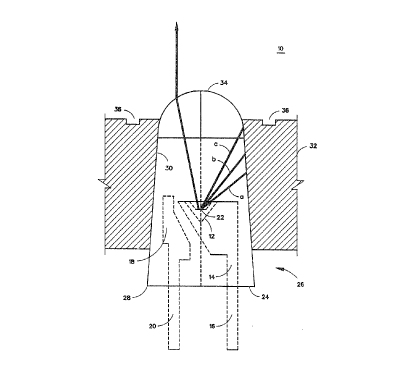
a in FIG: 2. Also, the encapsulating material
32 frustrates the total internal reflection of
class 2 and 4 rays at point b and point c,
respectively, in FIG. 2. This is accomplished
by lowering the internal reflectance from 100%
to the reflectance of the encapsulating
material 32>
The result of the use of the encapsulating
material is that only class 1 rays as
illustrated in FIG. 2 pass through the exposed
portion 34 of the epoxy resin envelope 26, and
these are the most useful and effective light
rays emitted by the LED 10. Thus, the
encapsulated LED 10 provides the best light
source for an instrument readhead by preventing
unwanted rays from exiting the LED 10.
Significantly less aperturing is required
in the illumination optics of an instrument
readhead in which the encapsulated LED 10 is
incorporated. This less apexturing allows more
of the class 1 rays to illuminate a sample.
For example, a computer simulation has shown
that a 2.5 to 3 fold increase in signal level
is possible by encapsulating a LED 10.
In order to insure that the class 2, class ,
3 and class 4 rays are prevented from exiting
the LED 10, the diameter d (FIGS. 3 and 4) of
the exposed portion 34 of the epoxy resin
envelope 26 must be calculated and maintained
during encapsulation. The diameter d of the
exposed portion 34 must be sized such that the
rays emitted from the active light emitting
MS 1660
y ~'7 ,7 rv L. r !°
element 22 that strike the surface of the epoxy
resin envelope 26 inside this diameter (for
example, ray 22-b in FIG. 3) are not internally
reflected, but are refr<zcted out of the epoxy
5 resin envelope 26 (for example, the ray b-c in
FIG. 3). In order to insure that a ray is not
internally reflected, the angle the ray makes
with a surface normal 38, such as the angle x
in FIGS. 3 and 4, must be less than a critical
10 angle given by the formula: sin(x) <1/n; where
n is the index of refraction of the epoxy
material of the envelope-26. If the worse case
ray 22-b-c shown in FTG. 4 is considered, from
the triangle b-o-a the formula can be written:
d/2 = r [sin (180-z)], but 180-z = x + y,
therefore, d = 2r[sin (x + y)]. From the law
of lines we know: rsin (x) = s [sin (y)], or:
y = arcsin [r (sin(x)/s)], and substitution
gives: d = 2r(sin (x + arcsin (r/s/n/))],
where x < arcsin (1/n). In a typical example
with r = .079 inch, s = .123 inch, and n = 1.5,
the equation results in x = 41.8 degrees and d
- 0.146 inch. Through this calculation, the
diameter d of the exposed portion 34 of the
preferred encapsulated LED 10 can be
determined, and encapsulated light emitting
diodes 10 can be manufactured in quantity with
consistency. The light emitting diodes 10 may
then be used in instrument readheads providing
the best available light source.
rIS 1660