Note: Descriptions are shown in the official language in which they were submitted.
2 0 6 ~ 5 9 3 CFO 8358 ~S-
-- 1 --
l Cantilever Unit and Atomic Force Microscope,
Magnetic Force Microscope, Reproducing
Apparatus and Information Processing
Apparatus Using the Cantilever Unit
BACKGROUND OF THE INVENTION
Field of the Invention
The present invention relates to a cantilever
unit in which a cantilever and a displacement amount
detecting means for it are integrated into one unit
to attain a reduction in size, and to an atomic force
microscope (hereinafter referred to simply as "AFM")
which uses such a cantilever unit to measure the three-
dimensional surface configuration of a specimen in
nanometer scale. Further, the present invention
relates to a reproducing apparatus and an information
processing apparatus utilizing such an AFM.
Related Background Art
An AFM detects an atomic force acting between
a specimen and a probe brought close to the surface
of the specimen, up to a position at a distance of
lnm or less therefrom, on the basis of the flexibility
amount (the displacement amount) of a cantilever ~an
elastic body) supporting the probe, and makes it
possible to observe the three-dimensional surface
configuration of the specimen at a resolution of lnm
or less by scanning the specimen surface while
206~9~
1 controlling the distance between the specimen and the
probe in such a manner as to maintain this atomic
force constant ~sinnig et al., "Phys. Rev. Lett."
_, 930 (1986)). Unlike a scanning tunneling
microscope (hereinafter referred to simply as "STM"),
the AFM does not require the specimen to be conductive,
so that it allows observation in atomic or molecular
order of the surface of insulating specimens, in
particular, the surface of semiconductor resists,
biopolymers or the like. Thus, the AFM is expected
to find a wide range of application.
Figs. 5 and 6 show conventional AFMs.
Basically, an AFM is composed of a probe 111 opposed
to the specimen surface, a cantilever 107 supporting
the probe, a means for detecting the amount of
displacement of the cantilever due to the atomic
force acting between the specimen and the probe, and
a means for three-dimensionally controlling the
relative position of the specimen with respect to the
probe.
In the conventional AFM shown in Fig. 5,
the detection of cantilever displacement amount is
effected by an optical lever method according to
which a light beam is applied from behind the
cantilever 107, obtaining the displacement amount
from the shift amount of the position of the reflected-
light spot. In the conventional AFM shown in Fig. 6,
2065~3
1 a tunnel-current method is adopted, according to
which a conductive probe 602 is arranged behind the
cantilever 107 at a position close to it, and position
control is performed on the conductive probe 602 in
such a manner that the tunnel current flowing between
the cantilever 107 and the conductive probe 602 is
maintained constant, obtaining the displacement amount
of the cantilever from the position control amount.
However, the optical lever method, described
above, requires an adjusting jig for causing the light
beam to be applied to the back surface of the
cantilever, an optical component such as a lens 502
or a mirror, and a position adjusting jig for a half-
split photodiode 504. The tunnel current method
requires a jig for adjusting the position of the
conductive probe 602 with respect to the back
surface of the cantilever. Thus, in both methods,
the mechanical structure of the cantilever displacement
amount detecting means has to be rather large and
complicated. As a result, the mechanical structure
of the displacement amount detecting means is subject
to positional deviation due to disturbances such as
floor vibration, acoustic vibration, or temperature
drift, or to generation of resonance due to
deterioration in rigidity, thus making it difficult
for the detection of the cantilever displacement
amount to be effected at a satisfactory level of
resolution.
206~93
1 SUMMARY OF THE INVENTION
It is an object of the present invention to
provide a cantilever unit in which the cantilever
displacement amount detecting means is integrated
with the cantilever and which is little subject to
the influence of disturbances.
Another object of the present invention is
provide an AFM which uses such a novel cantilever unit
and which requires no relative positioning and is
little subject to the influence of disturbances. Still
another object of the present invention is to provide
a reproducing apparatus utilizing this AF~ to
reproduce information recorded on a recording medium,
as well as an information processing apparatus in
which this AFM is combined with an STM.
In a first aspect of the present invention,
there is provided a cantilever unit comprising a
cantilever for supporting a probe and a displacement
amount detecting means, which displacement amount
detecting means is integrated with the cantilever.
In a second aspect of the present lnvention,
there is provided an information processing apparatus,
comprising a cantilever unit according to the first
aspect of the present invention.
In a third aspect of the present invention,
there is provided an information processing apparatus,
comprising a cantilever unit according to the first
2065~93
-- 5
1 aspect of the present invention and an information
recording medium stationed in close vicinity to said
unit, wherein an information in the medium is
reproduced at a signal on the basis of an displacement
S amount of the cantilever.
In a fourth aspect of the present invention,
there is provided an atomic force microscope comprising
a cantilever unit according to the first aspect of the
present invention.
In a fifth aspect of the present invention,
there is provided a magnetic force microscope
comprising a cantilever unit according to th~ first
aspect of the present invention.
In accordance with the present invention, the
optical-integrated-circuit technique is utilized to
optically integrate a light source, an optical
waveguide, a waveguide-type optical-path changing
device and a photodetector into one integral detection
unit, which is integrated with a cantilever, thereby
making it possible to reduce the size of the
displacement detecting means to 1/50 or less as
compared to that used in conventional AFMs.
Accordingly, the resonance frequency of the detecting
means can be increased to a value several tens times
larger than that in the conventional AFMs, thus
rendering the detecting means little subject to the
influence of disturbances.
20~93
1 More specifically, optical components, such as
a light source, an optical waveguide, a lens for
condensin~ the light in the optical waveguide, a beam
splitter for dividing or synthesizing a light beam, a
mirror for turning the direction of light, and optieal
parts such as a coupler for extracting light out of
the waveguide, a photodiode for detecting light
quantity, a photoelectric-eurrent amplifying cireuit,
a signal proeessing eircuit, ete. are integrated into
one unit, whieh is integrated with a eantilever.
BRIEF DESCRIPTION OF THE DRAWINGS
Fig. 1 is a diagram showing the eonstruetion
of an optically integrated cantilever unit according
to a first embodiment of the present invention.
Fig. 2 is a diagram showing the construetion
of an atomic foree mieroseope using the optieally
integrated eantilever unit according to the first
embodiment of the present invention;
Fig. 3 is a diagram showing the construction
of an optically integrated cantilever unit according
to a second embodiment of the present invention,
Fig. 4 is a diagram showing the construction
of a cantilever unit applied to an information
processing apparatus according to the other embodiment
of the present invention;
Fig~ 5 is a diagram showing a prior-art example
206~93
1 of a cantilever displacement amount detecting system
in an atomic force microscope; and
Fig. 6 is a diagram showing another prior-art
example of a cantilever displacement amount detecting
system in an atomic force microscope.
DETAILED DESCRIPTION OF THE PREFERRED EMBODIMENTS
The present invention will now be described
in more detail with reference to embodiments thereof.
First Embodiment
Fig. 1 shows the construction of a cantilever
unit according to an embodiment of the present
invention.
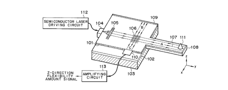
The cantilever unit shown includes a film
optical waveguide 101, an SiO2 layer 102, an Si
substrate 103, a semiconductor laser 104, a Fresnel
lens 105, a grating beam splitter 106, a cantilever
107, a reflecting mirror (a) indicated at 108, a
reflecting mirror (b) indicated at 109r a photodiode
110, a probe 111, a semiconductor laser driving
circuit 112, and an amplifying circuit 113.
In this embodiment, the semiconductor laser
104 is joined to one end surface of the SiO2/Si
substrate 103, on the surface of which is formed the
film optical waveguide 101, and serves to introduce a
laser beam into the optical waveguide 101. The
introduced laser beam is collimated by the Fresnel lens
2065~93
1 105, and is then separated into two rays in
different directions by the grating beam splitter 106.
One of the rays, indicated by the symbol A, passes
through the optical waveguide provided on the surface
of the cantilever 107 that is provided on the other
end surface of the Si substrate 103, and is reflected
by the reflecting mirror (a), 108, which is provided
on the free-end surface of the cantilever 107, to pass
backwards through the optical waveguide on the surface
of the cantilever 107 before it enters the grating
beam splitter 106 again.
The other ray of light, indicated by the
symbol B, whose course has been turned by 90~, is
reflected by the reflecting mirror (b), 109, and is
transmitted through the same course backwardly
before it enters the grating beam splitter 106 again.
The two rays are then synthesized by the grating beam
splitter 106 into a synthesized light C, which is
detected by the photodiode 110. When the probe 111
provided on the cantilever 107 detects an atomic
force to cause the tip end section of the cantilever
107 to be flexed in the Z-direction in the drawing,
a distortion corresponding to the displacement amount
~z is generated in the optical waveguide on the surface
of the cantilever 107, thereby changing the refractive
index of the optical waveguide. Assuming that this
change in refractive index is ~n, ~Z - cAn (wh~re c is
206~93
g
l a constant~, and a change of 2L~n (where L represents
the length of the cantilever) is generated in the
optical path difference between the ray of light A,
which passes through the surface layer of the
cantilever 107, and the ray of light B, which is
reflected by the reflecting mirror lO9, resulting
in a change in the luminous intensity of the synthesized
light C. Therefore, by detecting this change in
luminous intensity, it is possible to detect the
displacement amount in the Z-direction, ~Z, of the
tip end section of the cantilever 107. A signal
indicative of this change in luminous intensity is
amplified by the amplifying circuit 113 to become a
Z-direction displacement signal. Assuming that the
elastic constant in the Z-direction of the cantilever
107 is k, the magnitude f of the atomic force detected
by the probe 111 can be obtained by the equation:
f = k~Z.
A method of preparing such an optically
integrated cantilever unit will now be described.
A PiN photodiode is formed on an Si substrate
by the usual silicon processing. Then, a protective
Si3N4 film having a thickness of 0.1 ~m is formed
thereon by the LPCVD method. Next, after forming an
SiO2 film having a thickness of 0.5 ~m by thermal
oxidation on other opening sections, the Si3N4 ~ilm
is removed by piasma etching. Subsequently, an As2S3
2065~93
-- 10 -
1 film optical waveguide having a thickness of 1 ~m
is formed on the SiO2 film by vacuum evaporation,
and, bi utilizing the change in refractive index by
electron beam irradiation, a Fresnel lens and a
grating beam splitter are formed in the optical
waveguide. After patterning of configuration of a
cantilever, anisotropic etching is performed from
the back side of the substrate by using KOH solution,
thereby forming the cantilever. Then, a probe is
provided at the tip end of the cantilever by the
electron beam deposition method. After performing
cleavage on the chip thus obtained, a metal such as Al
is deposited on one end surface thereof and on a side
surface of the tip end portion of the cantilever to
form reflecting mirrors, and a semiconductor laser is
joined to the other end surface.
Next, the AFM of the present invention,
constructed by using the optical integrated cantilever
unit shown in Fig. 1, will be described with reference
to Fig. 2. A specimen 202 opposed to cantilever unit
201 of the type shown in Fig. 1 is brought near to
the probe 111 of the unit by means of an XYZ-drive
device 203, up to a position at a distance of lnm or
less therefrom. Due to the atomic force acting
between the probe 111 and the surface of the specimen
202, a deflection is generated in the cantilever. A
Z-direction feedback signal is supplied to the XYZ-drive
2065593
1 device 203 such that the amount of this deflection is
kept constant (i.e., the atomic force is kept
constant), thereby controlling the distance between
the probe 111 and the specimen 202. Further, a
scanning signal is supplied from a computer 205.
On the basis of this scanning signal, an X-direction
scanning signal and a Y-direction scanning signal are
supplied to the XYZ-drive device 203 by an X-direction
scanning signal circuit 206 and a Y-direction scanning
signal circuit 207, respectively, thereby scanning the
specimen 202 in the XYZ-dimensions relative to the
probe 111. In this process, it is possible to detect
the depth or height of the surface irregularities
from the Z-direction feedback signal for keeping the
deflection amount of the cantilever constant. In the
computer 205, two-dimensional distribution data on
the surface irregularities is obtained. The data is
displayed on a display 209. When a magnetic
substance, such as Fe, Co or Ni, is used here as
the material of the probe, a magnetic force microscope
is obtained, which makes it possible to observe the
magnetic domain structure of the surface of a magnetic
specimen.
Second Embodiment
Fig. 3 shows the construction of an optically
integrated cantilever unit according to a second
embodiment of the present invention. The cantilever
2065~93
-- 12 --
unit shown includes an SiO2/Si substrate (102'/103')
having on its surface a film optical waveguide 101,
into which a laser beam is introduced from a
semiconductor laser 112 joined to one end surface of
5 the substrate. The laser beam introduced is
collimated by a Fresnel lens 305, and is then
reflected by a reflecting mirror (c) indicated at 306
before it enters a grating coupler (a) indicated at
307. In the grating coupler (a), 307, part of the light
10 is extracted out of the optical waveguide, as indicated
by the symbol .A, and is reflected by the back surface
of the cantilever 107. After that, the part of the
light returns to the optical waveguide at a grating
coupler (b), indicated at 309, to be synthesized with
15 the ray of light B which has been propagated through
the optical waveguide, thus becoming a synthesized
light C, which is reflected by a reflected mirror (d),
indicated at 310, and then detected by the photodiode
110. When the probe 111 provided on the cantilever
20 107 detects an atomic force and causes the tip end
section of the cantilever 107 to be deflected in the
Z-direction in the drawing, there is generated, in
accordance with the displacement amount ~Z of the
cantilever, a change in the length of the optical
25 path through which the light portion A, extracted out
of the optical waveguide at the grating coupler (a),
307, returns to the optical waveguide at the grating
2065~93
- 13 -
1 coupler (b), 309. Assuming that this change is ~E,
there is generated, in the optical path difference
between the light A extracted out of the optical
waveguide and the light B which has been propagated
through the optical waveguide, a change AE = 2(1 -
n-sin~)~Z/cos~ (where ~ is the angle defined by the
normal of the optical waveguide surface and the
outgoing light A, and n is the refractive index of
the optical waveguide), thereby causing the luminous
intensity of the synthesized light C to change.
Therefore, by detecting this change in luminous
intensity, it i5 possible to detect the displacement
amount AZ in the Z-direction of the tip end section
of the cantilever 107. A signal indicative of this
change in luminous intensity is amplified by the
amplifying circuit 113 to become a Z-direction
dispalcement amount signal. Assuming that the
elastic constant in the Z-direction of the cantilever
107 is k, the magnitude f of the atomic force detected
by the probe 111 can be obtained from the equation:
f = k~Z.
Next, a method of producing the optical
integrated cantilever unit of this embodiment will be
described.
A PiN photodiode is formed on an Si substrate
by the usual silicon processing. Then, a protective
Si3N4 film having a thickness of 0.1 ~m is formed
2065~93
1 thereon by the LPCVD method. Next, after forming an
SiO2 film having a thickness of 2.5 ~m by thermal
oxidation on other opening sections, the SiO2 film is
removed ~y plasma etching. Subsequently, a glass-film
optical waveguide of 7059 Glass (manufactured by
Corning) having a thickness of 2 ~m is formed on the
SiO2 film by high-frequency sputtering, and, by
utilizing the change in refractive index by ion
exchange, ion implanation or the like, a Fresnel lens
and grating couplers are formed. Then, a chip having
a cantilever formed by patterning and anisotropic
etching on another Si substrate is joined to the glass-
film optical waveguide by anode bonding method. After
performing cleavage and polishing on the chip, a metal
such as Al is deposited on end surfaces thereof to
form reflecting mirrors, and a semiconductor laser is
joined to another end surface thereof.
Referring to Fig. 4j embodiment of information
processing (recording/reproducing) apparatus of the
present invention will be described in the following.
The same constitution of apparatus (not illustrated)
as in the above Fig. 2 is employed in the present
embodiment, too. In Fig. 4, probe 111 is formed of a
conductive material. Further, the cantilever unit is
arranged so that a tip of the probe is close to a
desired position on the surface of the information
recording medium (not illustrated), which corresponds
206~593
1 to the specimen 202 in Fig. 2.
Voltage for recording is applied between probe
111 and the above-mentioned medium by voltage applying
circuit for recording, to form a bit on the desired
position of the above-mentioned medium. Reference
numeral 317 indicates an Al wiring.
In the present invention, a material capable
of changing a form of own surface by current flowing
through the part was employed as medium as mentioned
above.
The operation reproducing the bits (information)
recorded on the above-mentioned medium in such a manner
is described below. The tip of the probe 111 is
stationed in close vicinity to the surface of the
lS above-mentioned medium, and the probe 111 is scanned
in a x-y direction in the figure. When the tip of the
probe 111 is made opposite to the above-mentioned bit,
the tip is stressed according to the shape of the bit,
whereby cantilever 107 is flexed. The amount of flex
is detected by the above-mentioned displacement
amount detecting means in the cantilever unit of the
present invention, to obtain the reproducing signal.
As mentioned above, the apparatus where the
recording of information is done by application of
2S the STM constitution and the reproducting of the
information is done by application of the AFM constituion
was explained.
2065593
1 As described above, in accordance with this
invention, the cantilever displacement amount
detecting system is formed as an integrated unit,
which is integrated with the cantilever, thereby
providing the following advantages:
(1) No relative positioning of the cantilever
and the displacement amount detecting system is needed,
thus attaining an improvement in maneuverability; and
(2) The apparatus as a whole can be reduced
in size and rendered less subject to the influence of
disturbances, thereby attaining an improvement in
detecting resolution and making it possible to measure
the three-dimensional surface configuration of a
specimen with an AFM of higher accuracy and higher
resolution.