Note: Descriptions are shown in the official language in which they were submitted.
20656~
Specification
Title of the Invention
Transistor Direct-Coupled Amplifier
Backqround o~ the Invention
The present invention relates to an amplifier
and, more particularly, to a transistor direct-coupled
amplifier for amplifying a DC balanced signal.
In general, although many types of monolithic
ICs called wide-range amplifie~s are used, when these
ICs are to be applied as wide-range amplifiers without
being matched with their characteristics, they may not
be used as the wide-range amplifiers due to no degree of
freedom of design. In contrast to this, in an amplifier
constituted by a combination of transistor circuits,
circuit design matched with an application purpose can
be obtained. Therefore, the amplifier is frequently
used in a video circuit and the like due to its high
degree of freedom of design.
2Q In a conventional direct-coupled amplifier, in
order to effectively use the dynamic range of an output
voltage to reach a power source voltage, when an
operating point is set to be about 1/2 the power source
voltage, variable resistors are used as some resistors
of a bias circuit and adjusted to absorb variations in
transistors and resistors.
2 0 ~ ~ ~ 3 ~
In the conventional direct-coupled amplifier,
when the operating point is set to be about 1/2 the
power source voltage, some of resistors of the bias
circuit must be changed into variable resistors VRll to
absorb variations in transistors and resistors, thereby
posing some problems in the manufacture of the
amplifier. In addition, after the variable resistors
are adjusted, the amplifier has no countermeasure
against a change in element value with time, a change in
power source voltage, and a change in temperature.
Especially, since a circuit having a high
voltage gain has a small input signal level, the circuit
is sensitive to a change in DC operating point caused by
these changes, a signal clamping distortion is
disadvantageously generated caused by a shift in the
operating point. In order to prevent this, an output
level must be set to be low, or a power source voltage
must be increased. These limitations are drawbacks in
use of the circuit.
Summary of the Invention
It is an object of the present invention to
provide a transistor direct-coupled amplifier capable of
optimally setting an output operating point to an
appropriate voltage at any time.
It is another object of the present invention
to provide a transistor direct-coupled amplifier
requiring no initial adjustment by a variable resistor.
-- 2 --
2 0 ~
It is still another object of the present
invention to provide a transistor direct-coupled
amplifier free from a change in element value with time,
a change in power source voltage, and a change in
temperature.
In order to achieve the above objects,
according to the present invention, there is provided a
transistor direct-coupled amplifier comprising a
positive-phase direct-coupled amplifier circuit using a
base of a first transistor as an input te in~l, a
second transistor having a collector connected to the
input t~rm; n~l of the positive-phase direct-coupled
amplifier circuit and an emitter connected to a
reference voltage source, the second transistor being
complementary with the first transistor, and a low-pass
filter for receiving an output from the positive-phase
direct-coupled amplifier circuit as an input, the
low-pass filter being connected to feed back an output
to a hase of the second transistor.
Brief DescriPtion of the Drawinqs
Fig. 1 is a circuit diagram showing an
amplifier according to an embodiment of the present
invention;
Fig. 2 is a circuit diagram showing a low-pass
filter shown in Fig. 1 according to the embodiment of
the present invention; and
2 ~ 3 ~
Fig. 3 is a circuit diagram showing a
conventional amplifier.
Description of the Preferred Embodiment
An embodiment of the present invention will be
described below with reference to the accompanying
drawings.
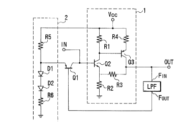
Fig. 1 is a circuit diagram showing an
amplifier according to the embodiment of the present
invention, and Fig. 2 is a circuit diagram showing a
low-pass filter LP~ having a resistor R0 and a capacitor
C0 in Fig. 1. A positive-phase direct-coupled amplifier
circuit 1 is constituted by an npn transistor Q2 and a
pnp transistor Q3. That is, a collector output from the
npn transistor Q2 is input to the base of the pnp
transistor Q3, and the collector of the pnp transistor
Q3 is connected to the emitter of the npn transistor Q2
through a resistor R3 and is negatively fed back.
Assuming that Rl = R3 = kR2 = kR4 (k is a constant >> 1,
Rl to R4: resistances of the resistors Rl to R4,
respectively), the gain of this circuit is about k
times.
A reference power source circuit 2 is
constituted by a series circuit. The series circuit is
obtained such that two resistors R5 and R6 each having
the same resistance and diodes Dl and D2 are arranged
between a positive power source termin~l Vcc (voltage:
Vcc) and ground. When the resistances of the resistors
2 ~ 3 ~
R5 and R6 are set to be low such that a change in
voltage caused by an emitter current of the transistor
Q1 can be neglected, a midpoint voltage of the diodes D1
and D2 goes to VCC/2~ and the emitter voltage of the pnp
transistor Ql goes to Vcc/2 + VD~ where VD represents an
ON voltage (about 0.6 V) of the diode Dl.
An operation of the circuit will be described
below. In the amplifier shown in Fig. 1, the pnp
transistor Q1 is normally set in an ON state for the
following reason. That is, if the pnp transistor Q1 is
set in an OFF state, the npn transistor Q2 has no base
current and is set in an OFF state, and the pnp
transistor Q3 has no base current and is set in an OFF
state. Therefore, currents from the two transistors Q2
and Q3 are not supplied to the resistors R2 and R3,
respectively, the voltage of an output terminal OUT goes
to 0 V, and an output voltage of 0 V appears at an
output te i n~ l FOUT of the low-pass filter LPF. At this
time, a current path is formed by the power source Vcc,
the resistor R5, the emitter-base path of the pnp
transistor Ql, the output terminal FOUT of the low-pass
filter I,PF, a resistor R0 (Fig. 2) in the low-pass
filter LPF, the input terminal FIN of the low-pass filter
LPF, the resistor R3, the resistor R2, and ground in
this order, and the pnp transistor Ql is turned on.
That is, the pnp transistor Q1 is not turned off but is
normally set in an ON state.
20~3a
An input signal to this amplifier is supplied
to an input terminal IN through an input capacitor (not
shown) not to influence an operating point of an input
stage. A DC balanced signal (DC component = 0) is used
as the input signal, a voltage equal to a DC voltage at
the operating point of the circuit output terminal is
generated at the output of the low-pass filter LPF
having a DC gain of 1 by removing a signal component.
This voltage becomes the base voltage of the pnp
transistor Ql, the value of the voltage is smaller than
that of the emitter voltage by a base-emitter voltage VBE
(about 0.6 V) of the pnp transistor Q1, and the value
(VCC/2 + VD - VBE) goes to about VCC/2 by canceling the ON
voltage VD of the diode Dl and the base-emitter voltage
15 VBE of the pnp transistor Ql. That is, the operating
point of the voltage at the output termi n~l OUT of th~
amplifier is Vcc/2. Therefore, the operating point is
proportion to the value Vcc in a change in power source
voltage, and the operating point is always set to be
Vcc/2
In case of a change in temperature, since the
ON voltage of the diode Dl and the base-emitter voltage
VBE of the pnp transistor Ql have the same temperature
coefficient, the changes in these voltages are canceled
each other. The operating point voltage of the circuit
output te ;n~1 OUT iS set to be Vcc/2.
20~3~
When a power source is charged, if the
operating point of the voltage at the circuit output
te in~l OUT is higher than VCC/2r the output voltage of
the low-pass filter LPF is higher than VCC/2~ thereby
turning off the pnp transistor Ql. At this time, as
described above, the voltage of the output terminal OUT
of this amplifier is decreased to be stabilized at a
point equal to VCC/2-
Since the input impedance of the low-pass
filter LPF is set to be higher than the output impedance
of the positive-phase direct-coupled amplifier circuit
not to influence a degree of voltage amplification, a
condition, i.e., ~the resistance of the resistor R0 >>
the resistance of the resistor R3", is selected.
Fig. 3 is a circuit diagram showing a
conventional direct-coupled amplifier. In Fig. 3, a pnp
transistor Q12 is used in the second stage of the
amplifier to increase utilization efficiency of the
power source voltage, and the amplifier has a circuit
arrangement suitable for requiring a large output
amplitude.
As described above, since optimal bias
conditions are different in accordance with transistors
used in the amplifier, a variable resistor VRll ~s
arranged in series with a resistor Rll to be adjusted.
As described above, according to the present
invention, an output from the positive-phase
-- 7 --
~06~fi~
direct-coupled amplifier circuit is fed back to an input
stage through a low-pass filter to perform DC feedback.
Therefore, an output operating point can be
automatically set to be an optimal voltage (in many
cases, about 1/2 the power source voltage) at any time.
Initial adjustment performed by a variable resistor is
not required, the output operating point can always be
kept at an optimal setting point which is designated in
advance in case of a change in power source voltage, a
change in temperature, and a change in element value
with time.