Note: Descriptions are shown in the official language in which they were submitted.
2 ~ 4 8
RD-20,183
CRO~S_RF1~E~E~CES TO ~ELA~En ~PPTIGATIONS
S This application is related to applications "SAMPLE
TIMING AND CARRIER FREQUENCY ESTIMATION CIRCUIT FOR SINE-COSINE
DETECTORS" by Sandeep Chennakeshu and G.J. Saulnier, Docket No.
RD-20,182 and "TANGENTAL TYPE DIFFERENTIAL DETECTOR FOR PULSE
SHAPED ~/4 SHIFTED DIFFERENTIALLY ENCODED QUADRATURE PHASE SHIFT
KEYING" by Sandeep Chennakeshu and G.J. Saulnier, Docket No. RD-
20,184 both filed simultaneously with this application, also
assigned to the present assignee. These applications are hereby
incorporated by reference.
_
F; eld o~ th~ In~ention
This invention relates to digital radio systems, and more
specifically, to demodulation of a transmitted signal and
synchronization between the transmitter and receiver of digital
radio systems.
Descr~p~iQn of Related Art
The U.S. digital cellular telephone system uses time
divis~on multiple access (TDMA) as the channel access method.
In this system, typically 3 to 6 users (data channels) share a
common 30 KHz channel. Each user transmits data in an assigned
~ime slot that is a part of a larger frame. Typically the gross
bit rate of the data to be transmitted over the mobile channel
is 48.6 kilobits per second (kbps). The modulation method is
~/4 shifted-Diff rentially Encoded Quadrature-Phase Shift Keying
2~5~8
RD-20,183
(DQPSK). A typical system uses a Square Root Raised Cosine
transmit pulse shape for a transmission signal with a roll-off
of 0.35, or an excess bandwidth of 35% to shape the transmitted
data. A filter having an impulse response match~d to the
transmit pulse shape is used in the receiver. Coherent
detection, differential detection, or discriminator detection
may be used to demodulate signals encoded by ~/4-shifted-DQPSK
techniques.
Disturbances due to multipath propagation affect the
digital cellular transmission and require the use of an
equalizer in the receiver. ~qualizers employ coherent
demodulation and are complex to implement. With present
technology, the complexity of an equalizer makes its use in
portable radio receivers impractical. For such applications a
digital discriminator or a differential detector is more
suitable. These receivers are relatively simple and can be
implemented on a commercial digital signal processor ~DSP),
which forms th~ core of a modern digital mobile radio receiver.
When transmission introduces echoes in the received signal,
due to multipath propagation, the bit error rate ~BER)
performance of these discriminators degrade very rapidly.
Multipath propagation manifests itself in dispersion of the
transmitted signal. This dispersion is characterized by a
quantity called delay spread. Delay spread can be defined as
the time interval between the first arriving signal and last
significant echo. However, in most regions of cellular
operation in the U.S., the root mean square ~RMS) delay spread
will not exceed 14 microseconds or approximately 34% of a symbol
duration at this transmission rate (see, T.S. Rappaport, S.Y.
Seidel and R. Singh, "900 MH7 Multipath Propagation Measurements
for U.S. Digital Cellular Radiotelephonen, IE~E Globecom
Conference Record, Vol. 1, pp. 3.2.1-3.2.6, Nov. 1989, Dallas,
Texas) and hence degradation can be expected to be within
acceptable limits.
2~6~8
~D-20,183
The conventional discriminator comprises the following sequence
of processing functions: limiting, differentiation, envelope
detection, and integration. Specifically, after the RF signal is
received, it is heterodyned down by conventional methods to an
intermediate rrequency (IF). The signal is then limited by
normalizing its amplitude to a constant value with a limiter. A
differentiator and an envelope detector convert frequency to a signal
voltage. This type of discriminator can also be used to demodulate
analog FM and digital ~/4-shifted-DQPSK signals (see, "Discussion of
~/4-Shifted-~QPSK", TR95.3.3/8~.3.14.5, submitted to TIA ~echnical
Subcommittee TR45.3, WG III, Modulation Task Group, March 14, 1989.
available from the Electronics Industries Assoc., Engineering Dept.,
2001 Eye Street, N.W., Washlngton, D.C. 20006).
A drawback to the above described conventional discriminator is
the presence of the limiter. The limiter makes the discriminator
sensitive to the pulse shaping roll-off fàctor of the transmitted
pulse signal. An increase in BER occurs by reducing the roll-off
factors or by reducing the excess bandwidth of the transmitted
signal. This puts a restriction on the data rate and the filtering
in the system.
A second deficiency in the conventional discriminator is the
inability to recover symbol timing and to correct carrier frequency
errors. Typically, thes~ conventional discriminators require
additional circuits having phase locked loops (PLLs) to perform these
2S functions.
It would be advantageous to create a simplified discriminator
that does not require a limiter, and is able to recover symbol timing
and to correct carrier frequency errors.
~UM~RY QF I~E~TIQN
A digital receiver employing a discriminator for
demodulating ~/4-shifted-DQPSK signals and pro~iding
synchronization in a TDMA system such as digital cellular
2~6~8
~D-20, 183
telephones also includes a heterodyne circuit for converting a
received radio frequency signal to an intermediate ~requenc~
(IF) signal. An analog-to-digital (A/D) converter circuit that
employs complex sampling of the IF signal is used to produce the
baseband (low pass) signal. This baseband signal comprises a
quadrature coefficient and an in-phase coefficient for each
sample of the IF signal. A predetermined number of samples
comprise a symbol. The number of samples per symbol is referred
to as N~. The samples are passed ~o a sorter circuit that
selects N~ samples per symbol to be used in the decoding.
A sample and phase adjustment (SPA) circuit receives a pair
of coefficients for each sample and N~ samples for each symbol
of the received signal. The SPA circuit selects samples for
decoding each symbol based upon sample timing. The SPA circuit
also receives as a feedbac~ signal, a carrier phase adjustment
and converts each sample it receives to a new quadrature
coefficient and in-phase coefficient based upon this adjustment.
A divider circuit receives the quadrature coefficient from
the SPA circuit, and divides it by its corresponding in-phase
coefficien~ to create an ou~put sample representing a tangent of
a signal phase angle for a portion of a symbol.
An inverse tangent circuit receives each tangent of the
signal phase angle and creates an output sample representing a
decoded phase angle.
A delay circuit delays the decoded phase angle for the
duration of a shor~ predetermined period and then passes it to a
summer circuit. The summer circuit receives the output sample
of the inverse tangent circuit and subtractc from it the output
sample of the delay circuit to create a relative phase angle.
A modulo-2~ correction circuit receives the relative phase
angle signal and corrects for wrap-around to create a corrected
- relative phase angle signal. Wrap-around occurs when the angles
straddle the 0 or 2~ radian point, where an inheren~
discontinuity Pxists. This discontinuity causes uncertainties
-- 4
%~ 8
RD-20,183
when a sample representing an angle that is between 0 and
radians is subtracted from a sample being be~ween ~ and 2
radians, or vice versa. The modulo 2~ correction circuit
corrects for this discontinuity. The relative phase angle
signal is sent to an integrate and dump filter ~IDF) that sums
the signal for all samples in a symbol period, then dumps the
sum to an output, the sum representing a symbol phase angle.
A four-phase decoder circuit receives the symbol phase
angle and de~odes the angle into a pair of bits that constitutes
the decoded information.
Adjustments to sample timing and carrier phase are
performed by an adjustment circuit that monitors the error
between the decoded symbol ~hase angle and a predetermined
information set (reference phase angles~ provided by the
preamble of each TDMA slot. The adjustment circuit provides the
sample timing and the carrier phase adjustment to the SPA
circuit. The SPA circuit chooses different samples to be
decoded based upon the sample timing from the adjustment
circuit. The SPA circuit uses the carrier phase adjustment and
recalculates a new quadrature coefficient and in-phase
coefficient for the new samples produced by the sorter circuit.
The new quadrature coefficients and in-phase coefficients are
passed to the divider circuit, the inverse tangent circuit, the
delay circuit, the IDF circuit and eventually to the adjustment
circuit, untiL the best sample timing adjustment and the best
carrier phase adjustment have been determined.
In an alternative embodiment, the carrier phase adjustment
is not performed by the SPA circuit and is performed by a
predecoding summer that adds the carrier phase adjustments to
the samples before being decoded by the four-phase decoder,
thereby reducing the degree of complexity in processing.
~- ~
2~648
RD-20,183
QB2E~TS OF THE INVE~ T ON
An object of the present invention is to create a
simplified receiver for digital radio systems that employs a
discriminator which does not require a limiter and is capable of
recovering symbol timing and correcting carrier frequency
errors.
Another object of the invention is ~o provide a
simplified receiver for digital radio systems that employs a
discriminator that is capable of decoding both digital and
analog signals.
A further object of the invention is to provide a
simplified receiver for digi,tal radio system~ that employs a
discriminator that can quickly adjust to frequency differences
between the transmitter and receiver oscilla~ors.
A further object of the invention is to provide a
simplified receiver for digital radio systems that employs a
discriminator having a reduced bit error rate that is not
sensitive to the degree of roll-off in the transmitted pulses.
The features of the invention believed to be novel are
set forth with particularity in the appended claims. The
invention itself, however, both as to organization and method of
operation, together with further o~ects and adv~ntages thereof~
may best be understood by reference to the following description
taken in conjunction with the accompanying drawings in which:
Fig. l is a block diagram of a generaLized digital
radio system.
Fig. 2a illustrates a TDMA frame structure.
Fig. 2b illustrates the Electronic-~ Industries Assoc.
IS-54 slot structure for base station to mobile station
-- 6 --
.
:
2~5~8
RD-20,183
transmission.
Fig. 3 is a block diagram of a prior art digital
discriminator.
Fig. 4 is a block diagram of the limitér of Fig. 3.
Fig. 5 is a simplified block diagram of a receiver
employing one embodiment of a discriminator of the present
invention.
Fig. 6a and 6b are graphical representations of the
carrier phase error incurred by carrier frequency offset, and
the carrier phase adjustmen~, respectively.
Fig. 7 is a simplified block diagram of a second
embodiment of a discriminator of the present invention.
Fig. 8a, 8b and 8c are illustrations of the variation
of optimal sampling points due to multipath propagation and
signal fading.
,
.
2 ~
RD-20,183
~ETATLEn ~ESCRIPTIQ~ QF ~E P~EFE~E~ EM~QnIME~T
Fig. 1 is a block diagram of a generalized digital radio
system. Transmitter 4 transmits an encoded digital signal via
radio waves as RF signal 5. This is received at an antenna 11
of receiver 9. The received RF signal, being approximately 900
MHz in frequency, is heterodyned down by heterodyne circuit 6 to
an IF frequency 3 of approximately 450-500 kH~ and supplied to
input 3 of an A/D converter 10 of discriminator 1.
Discriminator 1 decodes the IF signal into a signal which can be
utilized by output means 7. Output means 7 can be a speech
synthesizer and loudspeaker to produce audible speech, a digital
computer, or any other device which can make use of digital
data.
Fig. 2a illustrates a basic TDMA frame structure. The TDMA
frame structure 140 is broken down into a number o~ TDMA slots
142, 144, 146. Fig. 2b sho~s the ~lectronics Industries Assoc.
IS-54 slot structure (for example slot 2 of Fig. ~a) for base to
mobile transmissions usèd in U.S. digital cellular systems.
This slot structure, which is 324 bits in length, begins with a
preamble 166 being 28 bits long that contains synchronization
words. Twelve slow associated control channel (SACCH) bits 168
are next. Data bits 174, being 130 bits long, follow SACCH bits
168. Twelve Digital Verification Color Code (DVCC~ bits 176,
130 data bits 178 and twelve reserved bits 179 are at the end of
the ~lot.
A conventional discriminator can be realized digitally as
illustrated in Fig. 3. In this case the limiter must be employed at
the low-pass stage in the receiver due to the direc~ digital
conversion method used.
In the discriminator, an RF signal that has been converted ~o an
IF signal 303 is substantially digitized through A/D converter 310
into samples (I,Q). The sampling rate is governed by sampling clock
312 running at four times the IF frequency. Sorter 320 selects
2~6~
RD-20,183
samples (I',Q') to be used in decoding and discards the remaining
samples. The coefficients (I',Q') are sent to limiter 350.
The output signal I" from limiter 350 is multiplied in
multiplier 372 by the previous Q" sample that is temporarily held in
delay circuit 362. Similarly the output signal Q" is multiplied in
multiplier 374 with the previous I" sample which is held for a
temporary period in delay circuit 364. The output signals of
multipliers 372 and 374 are sent to summer 382 in which the signal
from multiplier 372 is subtracted from the signal from multiplier
374. Inverse sine circuit 390 receives the output signal of summer
382 and creates an output signal corresponding to an inverse sine of
the signals received.
Signal I" is multiplied at multiplier 378 by a previous
sample of I" that is held in delay circuit 368. Similarl~
multiplier 376 multiplies the output signal Q" by a previous
sample of Q" that is held in delay circuit 366. The output
signals of multipliers 376 and 378 are added in summer circuit
384 to produce an output signal that is received by the inverse
cosine circuit 395. The inverse cosine circuit 395 creates an
output signal that is related to its input signal by an inverse
cosine function. An integrator 400 receives the output siynals
of either the inverse sine circuit 390 or the inverse cosine
circuit 395 and sums all the signals over a sampling period. A
four-phase decoder 410 receives the output signal of the
2S integrator 400 and decodes the encoded phase into a pair of bits
for each symbol. (In the case of an analog FM signal the four~
phase decoder 410 and integrator 400 are not required.)
Fig. 4 is an expanded view of the limiter 350. A square
circuit 351 receives signal I' and squares the signal amplitude.
A second square circuit 352 receives signal Q' and squares the
signal amplitude. Summer 353 receives the signals from square
circuits 351 and 352 and adds the two amplitudes. Sum~er 353
passes its output signal to square root circuit 354 where the
square root of the output signal of summer 353 is taken.
2 a ~
RD-20,183
Inverter 355 creates an output signal that is the reciprocal of
its input signal and sends it to multipliers 359 and 361. The
output signal I" of multiplier 361 is original signal I' that is
multiplied by the signal from inverter 355. Similarly, the
output signal Q" of multiplier 359 is the product of Q' and the
output signal from inverter 355. The output signal of limiter
350 is a normalized signal, comprising the output signals of
multipliers 359 and 361.
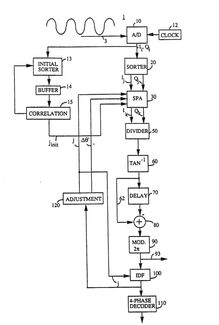
Fig. 5 is a partial block diagram of a digital
discriminator 1 employed in a receiver for digital radio systems
according to the present invention and as shown in Fig. 1. The
IF signal 3 is converted to baseband using direct digital
conversion. This conversion is accomplished by a flash A/D
converter circuit 10 sampling the signal at four times the IF
frequency or approximately 1800k samples/second. The sampling
rate is governed by a sampling clock 12. The samples are
quadrature phase shift keyed (QPSK) samples. The result is a
pair of coefficients from each sample, being an in-phase
coefficien~ Ii, and a quadrature coefficient Qi~ Of the baseband
~/4-shifted-DQPSK signal.
The discriminator operates by first establishing frame/slot
synchronization to find a rough sample index. This is done by
first selecting a number of samples with an initial sorter 13
and storing these samples in a buffer 14. A correlation circuit
}5 correlates a number of buffered samples pertaining to the
length of the preamble 166 of Fig. 2b starting from an index
with the predetermined preamble. The index marking the starting
sample from which the received signal was correlated is
incremented to the next sample. An appropriate number of
symbols are selected, starting from the sample marked by the
incremented index. This process o~ selecting samples and cross-
correlating them with the preamble is repeated for several
frames until the correlation produces several successive peaks
that exceed a certain predetermined threshvld. This sample
-- 10 --
2~S~
RD-20,183
index, iinit/ is assumed to be the beginning of a frame and slot
(hereinafter fram/slot). Since the number of samples in a frame
is known, the beginning of the next frame can be calculated by
incrementing the sample index by the number of samples that are
S in a frame. The correlation circuit then repeats the
correlation process at the new sample index. If the correlation
between the known preamble and the received symbols is above a
predetermined threshold at this index, it can be assumed that
this is the beginning of the next frame. If the correlation
between the received symbols and the preamble is below the
predetermined threshold, the search is started at the beginning
again. If three successive correlation peaks are ~ound, the
frame/slot synchronization is complete, and the sample index
iinit is used as a starting point for a fine ad~ustment called
symbol synchronization.
In symbol synchronization, a sorter circuit 20 processes
the sequential string of samples (Ii,Qi) by retaining a
predetermined number of samples and discarding the remaining
samples, since most of these samples are redundant. The samples
retained are determined by the sampling index j starting with
iinit- The embodiment of Fig. 5 starts with a total of ei~hty
samples per symbol and retains ten samples per symbol. The
number of samples discarded can be any number described by n
where n=2*i; and i=1,3,5,7,9 ... It must be noted that the
greater the number of samples discarded, the shorter the
processing time but the greater the timing error. A further
description of the functioning of the so~ter circuit, can be
found in "A VLSI demodulator for digital RF Network
Applications: Theory and Results", G.J. Saulnier et al., IEEE
Journal on Selected Areas in Communications, Vol. 8, No. 8, pp.
1500-1511 October 1990, which is hereby incorporated by
re~erence.
In the present invention, prior to establishing sample
timing it is necessary ~o synchronize to a TDMA frame/slot.
2 ~ 8
RD-20,183
This can be done using a correlation with the preamble sequence
contained within each slot. Assume that this timing can be
established to be within ~ N1 ~<N~) samples of the true
location, where N~ represents the number of samples per symbol.
The best sample timing location must be selected from:
j = jinit + nT/N9 (1)
where T is a symbol period, n=1,2,...N~ and jlnit is the sample
location corresponding to frameislot sync.
In order to establish sample timing, as described by
equation (1), and estimate carrier frequency offset, a 2-
dimensional search is performed to find the sample time and
phase rotation (corresponding to the frequency offset) that will
minimize the bit error rate.
The coefficients (Ij,Qj) that are retained by the sorter
circuit 20 for a given sample index j arè then selected in pairs
and adjusted for any frequency offset by the SPA circuit 30.
The SPA circuit 30 synthesizes a new pair of coefficients
(Ik,Qk) from coefficients (Ij,Qj) using an estimated phase
adjustment ~k. The resulting signal coefficients (Ik,Qk)
produced during a symbol interval are described below. (For
simplicity of notation and description it is implicitly assumed
that there is no fading or noise present in the system.) The
coefficients (Ik,Qk) produced during a symbol interval can be
represented as:
lk=gkcos(~k+ ~k-~9k+~) (2
Qk = gk sin(~k + ~ 9k + ~
where ~is an arbitrary phase, gk is the amplitude o~ the sampled
signal output (Ii, Qi) of A/D converter 10, ~k iS the information
bearing phase angle at the kth sampling instant of the sym~ol, ~k is
- 12 -
2~5~8
~D-20,183
the carrier phase rotation arising due to a frequency offset and ~k'
is the estimated phase adjustment to compensate for the offset
between transmitter and receiver carrier phase angles. ~ new set of
coefficients ~Ik,Qk) is synthesized to compensate ~or dif~erences in
reference oscillator frequencles between transmitter and receiver.
This difference causes continual phase shift differences which must
be compensated for to reduce errors.
Fig. 6a shows waveform 422 that represents the carrier waveform
as calculated by the receiver 9 of Fig. 1. Carrier waveform 424
represents the actual carrier waveform sent by transmitter 4 of Fig.
1. a~ is a phase difference between waveforms 422 and 424 at
sampling point 426 resulting from a slight difference in frequency
between the transmitter and receiver. This difference in frequency
may result from a mismatch in the oscillator frequencies of the
transmitter and receiver. The present invention compensates for this
phase shift ~by estimating the phase shif~ ~' and synthetically
shifting waveform 422 forward, as shown in Fig. 6b such that
waveforms 424 and 428 are in phase at sampling point 426.
The divider circuit 50 of Fig. 5 divides equation 2 by equation
1, or more specifically, divides coefficient Qk by Ik to produce an
output signal that represents a tangent of the signal phase angle,
namely:
= t~ (~k+~k-~k~E)
Ik (4)
In the discriminator of Fig. 5 the use of a divider circuit 50
replaces the need for a limiter in the discriminator circuit of Fig.
3. The divider sets ~he complex envelope of the (Ik,Qk) coefficient
pair to unity. In the absence of noise, the divider circuit 50
removes the dependence of the (Ik,Qk) coefficients on the amplitude
since divider output signal represents a ratio.
The inverse tangent circuit 60 produces an output signal
representing a phase angle that can be described s:
- 13 -
2 ~ ~ t~
RD-20, 183
t IQk = q)k + ~3k - ~k + E ( 5 ~
Summer circuit 80 subtracts an angle delayed by delay circuit 70
from the output signal 62 of the inverse tangent circuit 60
representing the decoded phase angle, to produce an output signal
representing a relative phase angle. This relative phase angle
signal (~k) can be represented as:
~q)k = (Pk - ~k~ + ~ ( 6)
where ~ is the phase rotation between two samples and is fixed, and
a~ is the corresponding fixed phase adjustment. Typically, Qk
corresponds to the sampling interval. ~k in the present embodiment
is equal to 1/10 of a symbol duration (T).
The relative phase angle signal is then received and
processed by a modulo-2~ correction circuit 90, al~ering the
phase of the signal as follows:
IF ~k ~-180THEN ~k = ~k +36~ (7a)
and
IF a~k > 180 THEN l~(l)k = a~k - 36no ~7b)
producing a corrected relative phase angle output signaL. This
correction reduces the BER when successive angles wrap-around ~he
real axis. The need for this correction is explained by the
following example: Let ~k = 5. ~k-~k = 355 and for convenience let
~ . Then, without the modulo-2~ correction circuit, ~k = -
350 when it should be a~k = 10. The modulo-2~ correction circuit
removes the wrap-around error.
- ' ': :.
2~6~8
RD--20, 183
The corrected relative phase angle signal is summed in the IDF
100 over a symbol period and then dumped.
N,+j-l
4k
k-j (8)
where, N~ is the number of samples per symbol (10 samples per symbol
in the present embodiment), ~ is the output 102 of the IDF 100
representing the sum or symbol phase angle and j is the sample index
corresponding to the start of a symbol period. ~k iS the relative
phase angle of the kth symbol
The symbol phase angle ~ represents a differentially encoded
~/4-shifted-DQPSK symbol and is decoded directly into a pair of bits
using a four-phase decoder 110. The decoder 110 determines into
which quadrant the corrected phase angle falls, and determines the
two-bit binary value corresponding to this quadrant. The quadrants
are numbered in a counter clockwise direction as 0-1-2-3. The
present invention employs a Gray coded transmitted bit stream having
quadrants numbered in a counter clockwise direction as 0-1-3-2. The
relative phase angles can take four values corresponding to the four
pairs of input bits (Xk,Yk). Table 1 indicates the mapping of the
pairs of bits onto the relative phase angles, using a Gray code.
~k X~
:~ 1 1
~ 0
+4 0 0
i~ I Q
Table 1 ~/4-Shifted-DQPSK Relative Phase Mapping
Symbol timing determined by sample index j and carrier phase
2 0 ~
RD-20,183
ad~ustment estimation ~ are critical in reducing the BER performance
of a digital discriminator. Symbol timing estimation corresponds to
determining the best sample in each symbol interval. Carrier
frequency offset ~ is manifested as a phase rotation of actual
symbol phases. ~ence, the estimation of carrier phase adjustment
corresponds to determining the phase adjustment per symbol period.
The present invention establishes sample timing and carrier
frequency offset error correction by minimizing the error between
differential phase angle of a preset synchronization word transmitted
as a preamble known to the receiver and a corresponding decoded phase
output signal from IDF 100. The process ma~ be mathematically
represented as:
. N;
n~n ( ~ [0i+ ~ i0]2}
{j,a~) i=2
where,
j = sample index,
~i = differential phase angle of ith symbol of preamble,
A~ = carrier phase adjustment given to received signal,
~a) = differentially decoded phase angle corresponding to the ith
symbol at the jth sampling index.
Np = number of symbols in the preamble.
If the magnitude of the phase jitter due to additive white
Gaussian Noise is less than ~/2 radians and there is no
intersymbol interference, then the metric given by equation (9)
is a rough approximation to choosing the largest maximum
likelihood estimate of the signal to noise ratio for each sample
time and frequency offset, averaged over the preamble.
The error minimization described by equation (9) provides an
estimate of the phase adjustment per symbol. The phase adjustment
per sample is obtained by dividing ~by Nq.
The error minimization described by ~9) is performed by
- 16 -
2 ~ '1 8
~D-20,183
adjustment circuit 120 shown in Fig. 5. Ad~ustment circuit 120
minimizPs the error by making adjustments to sample timing j and
carrier phase adjustment estimation ~. These adjustments are made
by performing a two-dimensional search over all sample timing
adjustments j and phase adjustments ~' for the minimum error value.
Adjustment circuit 120 and the loop in which it is contained
functions as follow~: The number o~ samples per symbol ~ is
predetermined. (In the present embodiment there are ten samples per
symbol.) The A/D converter circuit 10 and sorter circuit 20 output a
stream of coefficients (Ij,Q~) corresponding to each successive
symbol. Symbol timing is establi~hed by successive use of different
sample indices j, starting from iinit, followed by error calculations
pertaining to the index performed by adjustment circuit 120. The SPA
circuit 30 first applies a fixed carrier phase adjustment ~' to a
set of samples and produces a corresponding set of (Ik,Qk) pairs.
The sample set is comprised of samples pertaining to the present
index ta~en for all symbols in the preamble. The symbol decoding
error for this set of (Ik, Qk) pairs is determined by adjus~ment
circuit 120 accordin~ to the metric given by equation (9) and stored
therein. The sample timing index is incremented to its next value
and the process is repeated for the next sample set. This process is
continually repeated until all sample sets for the first fixed
carrier phase adjustment ~' have been decoded and the symbol
decoding errors have been determined.
The adjustment circuit 120 then appl$es the next ~ixed carrier
phase ad~ustment ~' to the next sample set and determines a
corresponding decoding error with the use of synchronization word
symbols in the preamble 166 of Fig. 2b known by the receiver. These
synchroniza~ion words are used as a reference to estimate the best
sample timing ~ and carrier phase ad~ustment ~H' that minimizes the
squared error between the relative phase angles of the reference
sequence and the corresponding relative phase angles of the detec~ed
sequence. The synchronization word symbols can also be used after
initial synchronization to fine tune the frame/slot synchronization.
- 17 -
2 ~
RD-20,183
After all fixed ca~rier phase adjustments ~ have been
applied, the value that minimizes the symbol decoding error is
determined. The symbol synchronization can be summarized as follows:
Each TDMA slot position (for example the second slot 144 of Fig. 2a)
S has a unique synchronization word or preamble 166 (Fig. 2b) that is
known to the receiver. Frame/slot synchronization as described above
must be established before TDMA data 174, 178 is acquired. The
coarse frame/slot position is accurate to within +Nl samples of the
correct position, where Nl< NJ2 and N5 is the number of samples per
symbol.
Having established frame/slot synchronization, N2 data samples
on either side of the established slot synchronization position are
stored in a buffer in adjustment circui~ 120 of Fig. 5; where N2 2 N1
(In the present embodiment N~ = 10 and hence 5 samples on either side
are stored in the buffer). Each buffered sample is then sequentially
used as the starting point by the SPA circuit 30, for locating the
optimum sample timing j and carrier phase adjustment ~. This can be
described as a 2-dimensional search to minimi2e the error described
by equation (9) with respect to symbol timing j and carrier phase
adjustment ~'. The carrier phase rotation ~0 is expected to remain
relatively constant over several hundred TDMA frames. Hence, for
symbol synchronization, the adjustment circuit needs only to perform
the 2-dimensional search for the optimum sample timing j and phase
adjustment ~ at start up or at hand-off, and subsequently fix the
phase adjustment A~ and search only for the optimum sampling instant
j at the start of each time slot.
It must be noted that the correlation between the preamble 166
of Fig. 2b and decoded sequences, which is the output signal of IDF
lO0 of Fig. 5, is maximized, and not the correlation between the
preamble 166 of Fig. 2b and ~eceived sequences 3 of Fig. 5. Thus the
present invention corrects for the characteristics of the
discriminator in finding the optimum sampling point j and phase
adjustment ~.
- 18 -
2 ~
RD-20,183
Since the additive white Gaussian noise is circularly symmetric,
the frequency offset correction ~ can be applied by a second
embodiment of the invention shown in Fig. 7, which adds the
corresponding phase angle a~ at the input of four-phase decoder 110.
The embodiment of Fig. 7 operates in the same manner as the
embodiment of Fig. 5 up to where the best sampling point j and best
phase adjustment ~' have been determined. Thereafter, summer 113
receives the output samples from IDF 100, and receives the best phase
adjustment ~' from adjustment circuit 120. The summer 113 adds the
best phase adjustment ~' to each sample before being sent to four-
phase decoder 110. The signal from summer 113 is also passed to the
adjustment circuit 120. The adjustment at summer 113 is a simple
addition of signals and does not involve complex processing.
Delay spread causes symbol errors. This effect can be mitigated
by using an equalizer. In the absence of an equalizer, the most
intuitive way of reducing BER would be to choose an optimal sampling
point to minimize the contributions of ad~acent symbols. Figs. 8a,
8b, and 8c illustrate the effect of a small delay spread on the
present invention. Two rays of a multipath system are assumed to be
received in three different situations as illustrated by Fig. 8a, 8b,
and 8c.
In Fig. 8a, an original received signal 194 is followed by a
delayed signal 196, an echo, of equal amplitude. Let the optimal
sampling point 192 pertain to the center of the combined waves 198.
In Fig. 8b, an original received signal 204 is followed by echo 206
of lesser amplitude. Now if the optimal sampling point 202 pertains
to the center of the combined waves 208, then the optimal sampling
point has shifted from point 192 to 202 due to the differences in
relative amplitudes between the original received signal and the
echo. Similarly, Fig. 8c shows an original received signal 214
followed by echo 216 of greater amplitude. If the optimal sampling
point 212 pertains to the center of the combined waves 218 in Fig.
8c, then the optimal sample timing 192, 202, 212 in each situation
represented by Figs. 8a, 8b, and 8c, respectively, varies with the
2 ~
RD-20,183
relative amplitudes o~ the signal and the corresponding delayed
signal.
The present invention implements optimal sample timing
estimation, ma~ing the discriminato~ more robust to delay spread.
However, this action is only useful for delay spreads of
approximately one to two tenths of a symbol period. Moreover, the
minimization performed by the adjustment circuit 120 of Figs. 5 and 7
operates on the data of preamble sequence 166 of Fig. 2b.
The digital discriminator of the inven~ion, when employed in a
cellular telephone receiver, eliminates need for a limiter and hence
does not place severe restrictions on data rate and constraints on
filtering. Elimination of the limiter by implementing the digital
discriminator of the invention reduces the overall processing
requirements. The discriminator 1 employs an adjustment circuit 120
that performs integrated sample timing j and carrier frequency error
estimation ~. The sample timing recovery scheme reduces the BER
performance of the discriminator when there is a small amount of
delay spread.
The present invention can be used to de~odulate analog FM
signals that are commonly employed in conventional FM radio
broadcasts since it employs a differentiation type demodulation
scheme. To receive conventional FM radio broadcasts, the adjustment
circuit 120, and the SPA circuit must be deactivated in order not to
adjust the sample timing ; and phase adjustment ~'. An output 93 of
the modulo-2~ correction circuit 90 of Figs. 5 and 7 is used as ~he
output of the discriminator. The number of samples processed per
symbol must also be increased. The discriminator now may be used for
receiving analog FM radio signals.
The foregoing describes a digital radio receiver that
avoids the need for a limiter by incorporating an adjustment
circuit that adjusts sampling timing j and carrier phase
adjustment. The 3ER performance of the discrimina~or in such
that it can be used in mobile receivers where complexity has to
be low and where the delay spread is less than 0.2 of a symbol
-- ~0 --
2 ~ 8
RD-20,183
duration. The discriminator will also be useful in portable
radio applications where complexity is low and delay spread
relative to the symbol period does not exceed 10%.
The digital discriminator can receive conventional analog FM
radio broadcasts by deactivating the adjustment circuit, the SPA
circuit, IDF and the four-phase decoder. The digital di~criminator
also can also decode other digital modulation schemes, such as four-
level digital FM and four-level continuous phase frequency shift
keying (CPFSK~ ~ith modulation index h=0.25, which can be represented
as quadrature phase signals.
While only certain preferred features of the invention have been
illustrated and described herein, many modifications and changes will
occur to those skilled in the art. It is, therefore, to be
understood that the appended claims are intended to cover all such
modifications and changes as fall within the true spirit of the
invention.
- 21 -