Note: Descriptions are shown in the official language in which they were submitted.
-~065857
LATCHED ACCUMULATOR FRACIIONAL N SYNTHESIS
SW~TH RESIDIJAL ERROR R~DUCTION
Rac~round of the Invention
1 0
This invention relates generally to frequency
synthesizers and more particularly to a l~tohe l accumulator
fractional-N frequency synthes;zer employing more than one
latched accumuaator configuration, in which the rem~ining
15 noise components from the fractior-~li7~tion process are
coupled to a digital to analog converter and subsequently
applied to the phase detector output for r~n~Pll~tion of the
re~ l noise. The latched configuration operates
synchronously and enables the system to operate at higher
20 frequencies thereby reducing gpurious ~
Phase Tocked loop (PLL) ~equency synthesis is a well
known te-~hni~ue for generating one of many related gi~ns-l~
f~om a voltage controlled oscill~tor (VCO). In a single loop
PLL, an output signal from the VCO is coupled to a
programm~ble frequency divider ~vhich divides by a selected
A
Z06S8~ CE00210R
integer nu_ber to provide a frequency divided signal to a
phase detector which compares the frequency divided signal to
a ~efelellce signal from another fixed frequency os~illP~tor
5 which, often, is selected for stability of frequency over time and
environmçnt~l changes. Any difference in phase between the
frequency divided signal and the reference signal is output
from the phase detector, coupled through a loop filter, and
applied to the VC0 in a m~nner which causes the output
1 0 signal from the VC0 to change in frequency such that the
phase error between the frequency divided signal and the
reference signal is minimi~ed. Since the progrAmm~ble
divider divides by integers only, the output frequency step size
is constrained to be equal to the reference signal frequency.
15 With the single loop PLL, an engineering compromise must
be struck between the competing requiremsn~ of loop lock
time, output frequency step size, noise ~e~ro~ nce~ and
spurious signal generation.
In order to ovelco~e the li_itations of the single loop
2 0 PLL, progr~mmable frequency dividers c~pable of dividing by
non-integers have been developed. Output frequency step sizes
which are fractions of the reference signal frequency are
obtained while maint~ining a high reference frequency and
wide loop bandwidth. A discussion of fr~ction~ N synthesis
2 5 m~y be found in U.S. Patent No. 4,816,774. As described
therein, two accumulators are employed to simulate the
perfolmance of fractional synthesis of the switching between
di~e~nt integer values of divisors without the ~tten~l~nt
spurious ~ignal~ generated by such switching. The two~ 0 accumulator technique acts to reduce the unwanted spurious
by r~ncell~tion and loop filter rejection. Furthe~nore,
residual noise cancellation by application of the ripple
accumulator contents to a digital to ~n~lo~ converter
co~nected to the loop filter has been ~ closed in U.S. Patent
2~S58~5i7 ~
CE00210R
No. 4,204,174 but this implementation suffers from the
problem of not providing an exact cG-~ec1ion to the residual
noise waveform. A modification to a two ripple-accumulator
5 structure with accurate correction was di~closed in U.S.
Patent No. 4,758,802 but the implçment~tion is not ~mPn~hle to
higher order accumulator networks.
The reference signal frequency for the fr~ction~1-N
frequency srthe~i7er is, therefore, determined by the step
1 0 size of the VC0 output frequency multiplied by the
omin~tor of the progr~mm~hle divider divisor. Fractional-
N synthesis allows the use of a referencs frequency which is
much higher than the actual ch~nnel spacing and allows
~e~ign~ to use wider bandwidths due to the reduction of low
1 5 frequency spurious outputs. Wider bandwidths allow fast lock
times and the possibility of wideband mod~ ;nn applied to
the refe~nce input or the fractional division scheme.
Unfortunately, the system is not perfect and generates
some spurious sign~1s output at a frequency equal to the
2 0 ch~nnel spacing. The desired signal output purity is better
than the non-fractional system, but by itself may still be
insufficient for some high quality systems.
In order to minimi7e the effects of this spurious output,
two accumulator fractional-N synthesis systems have been
2 5 developed which spread out the spurious si~n~ls to
freq11~n~ies at which filtering is ine~pen~ive and simple. By
using &yalems with more than two accumulators this benefit
can be dr~m~t;c~lly increased.
The present multiple accumulator syste_s all have a
3 0 drawback in that the accumulators "ripple" the data. In
other words, on every clock pulse the data must act on the
entire digital network structure. This results in a relat*ely
low upper frequency limit of operation for a multiple
2~65857 CE00210R
accumulator system due to propagation delays in the digital
circuitry used to build the system.
The basic structure of a one-accumulator fractional N
5 system is shown in the block diagram of FIG. 1. A VCO 101
generates an output signal which, typically is coupled to a
progr~mm~hle frequency divider 103 which has an output to a
phase detector (O 105. The control input i9 a sllmm~tion of a
coarse ch~nnsl setting and the output of the digital netwo~L
1 0 which provides the fractional part of the division. The phase
detector 105 collv~:lltionally compares the phase of the divided
frequency, fv~ to the phase of the reference 9ignal ~requency fr
output from a reference os~ tor 107 to produce a signal
which i8 applied to a loop filter 109 and sllhsequently to the
1 5 VCO 101 to phase-lock the VCO output signal.
The selection of the divisor value of variable frequency
divider 103 is made by digital network 111 which, in previously
known implementations such as described in Z-transform
equivalent in United States Patent No. 4,758,802, comprises a
2 0 conventional adder 113, a comp~rator 115 (which produces a
"carry out" signal when the input to the comp~rator 115
e~cee-l~ a given numerical value), and fee~lh~ck logic 117
which subtracts the denominator (if a carry output occurs)
from the digital number representation output from adder 113
2 5 and compiqrator 115 before applying the digital number
Lc3entation to the adder 113. A second digital number
3ent~t;0n~ which in a fractional-N srt~esi~er is the
digital equivalent of the first differential of the offset phase
with respect to time (the offset frequency), is applied to another
3 0 input of the digital nelwol~ 111. The overall effect of the
digital netwo~L 111 is to integrate the differential phase and to
apply to the PLL a control signal (in the form of a carry-out
digital signal) which is a first order equivalent of the phase
offset. The adder 113 sums the previous contents of the adder
- ;~O6~8S~ CE00210R
113 with a d~/dt ( a numerator) on each occurrence of the
lefelence frequency signal fr. As described in U.S. Patent
No. 4,816,774, the adder 113 output is comp~red to a nu_ber (a
5 ~lenomin~tor of a desired fractional part of the divisor when
the divisor of frequency divider 103 is expressed as a su_ of a
whole number and a dennOmmeiraabbrr )- If the contenta of adder 113
çYcee-l the ~len~min~tor then the carry output is set true and
the contents of the adder is reduced by the ~lenQmin~t~r in
1 0 fee~lh~k logic 117 before the next reference pulse occurs.
As an exa_ple, assume the ~lenomin~tQr i9 13 and the
nu_erator is 1. On every thirteenth reference pulse the
adder 113 exceeds the tlenomin~tor and generates a carry
output which will increase the divisor of the frequency divider
1 5 103 by one for one reference si~n~l, fr, pulse. This removes
one pulse from the VCO 101 output signal and thus reduces
the accumulated phase error by 360 degrees. This corresponds
to a V13 division added to the nominal loop division number.
Shown in the Ztransform diagram of FIG. 2, is a Z-
2 0 transform equivalent digital network 111' of this one
acctlm~ t~r system consistent with that disclosed in U.S.
Patent No. 4,758,802. The Z-transform equation for the single
accumulator system is:
Q(l-z-l)+DI l
(2-zl) (2-z-l)
The Z-transfoIm adder 201 is fed from the numerator (minus
the denomin~tor if an overflow occurs) and the previous adder
content~ ~epre~ente~l by a z-1 (delay) block 203, 205. The
3 o ~QmpA~igon ig considered to be a digital slicer with
qll~nti7~tion error Q added at 207. The output from adder 207
is the digital number fed back to adder 201 and the carry out
signal is taken as the output signal. For Z-transform
CE00210R
analysis, howt:ver, no difference need be made between the
output and the feedback sign~l~
At point B an equation can be written as follows.
B(z)=B(z) z-1 +A(z) or B(z)-A(z)/(1-z-1)
But Data out=B(z)+Q and A(z)=Data in -B(z~Q
1 0 Sub~liluli.lg this in and solving for B(z) then:
B(z)=Dataint(2-z~l) - Q/(2-z-1)
And solving for Data out:
1 5
Data out = Data in/(2-z~l) + Q(l-z~l)/(2-z~l)
This equation may now be collvel led to the frequency
~l~mAin (Note that "v" is frequency norm~li7e~1 to the folding
2 0 frequency):
P~ Outl _ 1
I DataIn 1 115-4cos(
/ 2 - 2cos(~v
Q I ~ S-4cos(7~v)
Thus, the data into adder 201 is slightly low pass filtered
and the quanti7~tion noise introduced by the digital nelwoll~
111' is high pass filtered. The high pass filtering of the
qtt~3nti7~tion noige has the effect of reducing the spurious
3 0 sign~ls OCCUl.;llg at the frequency of the l~h~nnel to ch~nnel
frequency sp~ctng of the transceiver if the spurious occurs at
a frequency much below the corner of the high pass. By
select;ng a PLL respon~e with a low pass corner frequency
- 2~6~7 CE00210R
much lower in frequency than the high pass corner it is
possible to reject almost all of the noise. In a single
aCcltmlllatQr system, the high pass roll-off i8 20 dB/ lec~de.
5 Thus the reference frequency must be large to push the high
pass corner to large frequencies if sufficient noise suppre~sion
i8 to be obt~inerl (Or the PLL low pass must be very low in
frequency and thus lose the benefits of wide bandwidth.)
To improve the high pass filtering of the basic
1 0 fr~ct;on~l-N structure, it has been known to use fractional-N
synthesis for systems using more than one ~ccllm~ tor. A
two accllmnl~tQr fractional-N srthe~i~er is ~3isrlose~l in U.S.
Patent No. 4,204,174. Also, an eY~mrle of a multiaccumulator
fractional-N synthesi7er is shown in the block diagram of
1 5 FIG. 3, where the single digital network 111 of FIG. 1 is
m~nted by additional accumulators, in this instance,
accumulator 303, accumulator 305, and accumulator 307.
In a mult;~ccllmulator system, the contents of the first
~ccllmlll~tor 111 becomes the Data input to the second
2 0 accumulator 303. The contents of the secon~l accumulator 303
becomes the data input to the third accumulator 305. Once the
data is set at the output of adder 113 of ~ccllmlll~tor 111, it
must be transferred to the data input of adder 113 of
accumulator 303. Once the data is set at the output of adder
2 5 113 of accumulator 303, it must be tran~re.~ed to the data
input of accumulator 305, etc. All of the transfer must be
omrli~he~l in one clock pulse (which is typically derived
from the output of frequency divider 103). This process has
been termed a "ripple" process, and the accumulators are
3 0 known as "ripple" accumulators. Obviously, an upper limit
on the speed and/or the number of accumulators is imrose~l by
the ripple process.
The second accumulator 303 has its own Z-transform
quantization error, Q2, in addition to the error of, Q1, the first
BS~ CE00210R
accumulator. However the combinstion of these errors will
be greatly reduced from the single accumulator case. The
carry-output from the seconcl accumulator 303 i8 ~p~lie~3 to a
5 delay logic element 309 and, after the tli~erant;st;on protlllce-l
by delay element 309, is applied to adder 311. The carry output
from the comp~rator of accumulator 305 is twice differentiated
by delay logic elements 313 and 315 and input to adder 311.
The carry output from the comparator of accumulator 307 is
1 0 thrice di~elm.ti~ste~l by delay logic elem~nt~ 317,319, and 321
and input to adder 311. The carry o~ll.uts~ di~ele~iated as
described are added and output a~ an effective carry-out signal
to be applied to frequency divider 103. Thus, the effect
produced by the multiple accumulator system is to add the
1 5 first order phase offset of the carry-output of accllmulator 111
and the seco~d order phase offset of the differentiated carry-
output of accumulator 303, the third order phase offset of the
twice differentiated carry output of accumulator 305, and the
fourth order phase offset of the thrice differenti~te~3 carry
2 0 output of accumulator 307 for the effective carry-out ~n~l.
For simplicity, the Z-transform model of the first and
secon~l accllmlll~tQrs is shown in the diagram of FIG. 4. DO1
is the Data out of the first accumulator. From the above
calculation:
DOl = Data Out = Data In + Ql (l z-l )
(2 z-l) (2 z-l)
Di2 is the accumulator contents of the first
accumulator:
Di2 (Data In - DOl)
(1 - Z 1)
2~6~585~ CE00210R
A ~imilAr equation to that above for DO2 i8:
DO2= Di2 +Q2(l-z-
(2 z-l) (2
Substituting in the expression for Di2 and then
substituting in for DO1:
DO2 = - Ql~ l + Q2[ Z ]
(2_Z-l)(l z-l) l(2 Z-l)2~ 2 z-l (2-z-l)2(1 z
1 0
But: DO3 = DO2(1-z-1) and Data out = DO1 + DO3
Thus after some algebra:
1 5
Data Out = Data ~ 3 - 2z-l2l + Ql (1 z-l ~2 Q [(1 z-l ~2]
l(2 z-l) J (2 zl)2 2 - z-l
This representation is then converted to the frequency
2 0 ~om~in (Once again "v" is the frequency norm~li7e-1 to the
folding frequency):
Outl_~13-12cos(~rv
Data In 5 - 4cos(~
~ Ou~ = 2 - 2cos
2 5 I Q1 1 5 - 4cos(
~Outl_ 2- 2cos(~
Q2 I Ys - 4cos(7~v)
In this case the high pass corner occurs at about the
3 0 s~me frequency as in the one accumulator case but the
CE00210R
- ~;5~7
frequency response of the high pass characteristic to the
quantization noise is 40db/decade. This allows the PLL to have
a wider bandwidth, i.e., allows the fractional system to
5 operate at a lower frequency, than in the one accumulator
case while still maint~inin~ the desired noise suppression.
The number of accumulators can theoretically be
increased to any desired order. The resulting slope of the
response of the high pass characteristic to the q11~nti7Ation
1 0 noise will be the number of accumulators times 20db/ lerAtle.
The accumulators are "recombined" in what is known as a
"Pascal's triangle method" as disclosed in U.S. Patent No.
~,609,881. In general the higher order accumulators are
recomhine~l a8 (l z-1)(n-1)
1 5 The aforemPntisnefl systems require that the data must
ripple through all of the accumulators upon a clock pulse.
For a higher order system this requirement limits the
m~Yimum accumulator clock rate and thus limits the noise
ression which can be obtained. The reason for this limit
2 0 is that the propagation delay of each accumulator will add
until the data cannot ripple through the system in one clock
pulse period. Furthermore, even after proce~ir~ by multiple
~cc~m~ tQrs, a residual noise term will still remain which
may cause ~Yces~ive spurious si~n~1s in some applications.
-mm~ry of ~h~ Invention
A fractional-N latched accumulator synthç~i~er having
reduced resi~ 1 error accepts a digital mlmber to select a
3 0 contro11~hle os~ t~r output signal frequency. The output
signal frequency is frequency divided with a variable divisor
divider controlled by carry output ~ from lAtche~l
accumulator networks and a control siEn~1, which is
filtered by a loop filter, is applied to the controllable
CE00210R
oscillator. A first latched output signal related to the digital
number is generated and a second l~tchefl output siFn~l,
which i8 sn integral of said first l~tch~ output sign~l, is
5 generated. The first latched output signal and the seconll
l~tche~l output signal are combine~l to generate a residual
error correction ~ign~l The residual error signal i8 then
coupled to the loop filter.
1 0 Rrief Description of the Drawin~s
FIG.lis a block diagram of a first order fractional-N
synthesizer.
FIG.2is a Z-transform diagram equivalent of the digital
15 network in FIG.l.
FIG.3 is a block diagram of a multiple order ripple
fractional-N synthesizer.
FIG.4. is a Z-transform diagram equivalent of the
digital nelwo.L of a second order ripple accumulator.
FIG. 5 is a block diagram of a radio transceiver which
mPy employ the present invention.
FIG.6is a block diagram of a multiple l~tche-l
accumulator fractional-N synthesi7er in accordance with the
present invention.
2 5 FIG.7 is a block diagram detail of a delay ~c~ ng~ or
ripple, accumulator structure.
FIG;8 is a block diagram detail of a non delay ~A~ling or
~tGhe-l accumulator structure which may be employed in the
present invention.
FIG.9 shows a Z-transform diagram equivalent of the
l~tche~l ~ccl~m~ tor in FIG.8.
FIG.lOis the Z-transform diagram equivalent of a
three accumulator system in accordance with the present
invention.
~06~7 CE00210R
FIG. 11 shows the attenuation due to the digital nelwo,L
of the data in and the qll~nti~tion noise terms for a three
accumulator system in which the input data i8 not distorted at
5 higher frequencies.
FIG. 12 is a block diagram of a fractional-N srthesi7er
in accordance with the present invention and in which a
digital correction term i8 derived and applied to the phase
detector output through an analog differenti~tiQn network.
1 0 FIG. 13 is a block diagram of an alternative
~mho~liment of a fractional-N synthe.si7er in accordance with
the present invention and in which a digital correction term is
derived and applied to the phase detector output through a
digital differentiation network.
1 5
net~ile-3 Desc,l~l,ion of the Preferred li~mho~lim~nt
A basic block diagram of a radio transceiver which may
employ the present invention is shown in FIG. 5. Such a radio
2 0 transceiver, preferably, is a digital radio transceiver useful in
a digital radiotelephone system. The output of the srthesi~;er
503 is used by both the receiver 505 and the transmitter 507 to
produce a local oscillator and a transmit ~i n~l, respectively.
Control over functions of the transceiver, such as rh~nnel of
2 5 operation frequency, is provided by control logic 509 function
and is input to the first accllmulator of a fraction~l-N
srthesi7er as Numerator data in.
A multiple latched accumulator fractional-N
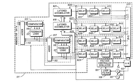
8~1the~i7er i8 shown in FIG. 6. The frequency srthesi7er
3 0 lltili7es a voltage controlled oscillator, VCO 101, which
provides the desired output frequency fo, as well as feeds the
input to a variable digital frequency divider circuit 103. The
output of the variable frequency divider 103 feeds one input of a
phase comp~rator circuit 105 with the other input being fed
2~6585~ L~
CE00210R
from a reference oscillator 107. The output of the phase
c~ A ~ ator 105 is filtered to remove extraneous noise
entq by loop filter 109. The output of the loop filter 109
5 i8 then fed back to the control input of the VCO 101 such that
the VCO 101 will adjust its output frequency fO to be equal to
the frequency of the reference oscill~tQr 107 times the digital
division ratio of the frequency divider 103.
In the preferred embo~liment, the division ratio, N, of
1 0 the frequency divider 103 is varied with a periodic sequence
such that the output frequency fO of the VCO 101 may be
adjusted in frequency steps equal to a fraction of the frequency
of the reference oscillator 107. This periodic sequence is
generated by a multiple accumulator digital netwolh 611. A
1 5 digitA~ nelwolh of four accumulators i9 shown in FIG. 6.
Numerator data, which corresponds to frequency offset
and which may include modulation information, is input
from frequency selection circuitry (not shown) and applied to
the first adder 113 of accumulator 615. The data output from
2 0 the first accumulator 615 is taken at the output of fee~lh~ck
logic 117 after processing by comparator 115. This data output
is available after the clock input si~n~l, derived from
frequency divider 103, has clocked the accumulator 615. It is
an important feature of the present invention that the data
2 5 presented from one accumulator to the next is only
transferred to the next accumulator in the string during one
clock cycle thereby avoiding the problem of having to ripple
through all accumulators during one clock pulse. Each
S~rc~ tor beyond the first is fed with the contents of the
3 0 next lower order accumulator. Each accumulator perfor~l~s a
digital integration of the contents of the accumulator of next
lower order with the first accumulator 615 performing a
digital integration of the input Numerator data. The secon~
accumulator 617 performs a double integral of the input
2~ CE00210R
Numerator data, the third accumulator 619 performs a triple
integral of the input Numerator data, and the fourth
accumulator 621 performs a quadruple integral of the input
Numerator data.
The output of each accumulator is the carry or overflow
output. For the first accumulator 615 this output signifies that
the output frequency fO of the VCO 101 has acq~ ed 360
degrees of phase error relative to the frequency of the signal
1 0 output from the reference oscillator 107. In order to correct
this, the division ratio of the frequency divider 103 is increased
by one integer for the next clock interval and the internal
contents of Ac~lm~ tor 615 is reduced by it's cspacity. This
action effectively removes one cycle of the output frequency fO
1 5 from the phase detector 105 input and thus results in a phase
CO~ lion of 360 degrees at the VCO 101 output. This
collection will occur only at the point the output frequency fO
would achieve 360 degrees of phase error without a loop filter
109. Such a condition will result in a sawtooth type of
2 0 waveform at the output of the phase detector 105 which must
then be filtered by the loop filter 109. The average value of this
sawtooth waveform is the correct control signal to select
frequencies which are spaced at fractional incrçmçnts of the
lefe~ellce frequency output from reference oscillAtor 107.
2 5 However, the internal contents of the first accumulator
615 represent the inter_ediate phase error. ~igher order
accu_ulators are included to operate on the internal contents
of the first accumulator 615 to provide interme~ te
co.lect;on~ to the phase error with the result that the sawtooth
3 0 type of wa~efoll~l can be subdivided in frequency, resulting in
lower noise output at the fundamental &equency of the
original sawtooth waveform.
The output of the higher order accumulators are fed
through digital delay networks (623, 625, 627, 629 respectively),
- 2Q6~i~57 CE00210R
which perform derivatives of the carry outputs. Since these
carry outputs of the accumulators are digital integrations of
the Numerator data input, the net result is higher order
5 corrections to the desired phase.
For eY~mple, the carry output of the secQn~l
s~rcllmul:ltor 617 is applied to digital delay nelwo~l~ 625 where
it i8 delayed by collventional delay elem~nt~ 631, 632, and 633
prior to being fed to a conventional digital adder 635. In adder
1 0 635, the delayed output of second accumulator 617 is added to
the negative of its previous value obtained from the output of
collventional delay element 637. This i8 a first derivative in a
digital sense. Since the output of the second accumulator 617
is the secQn~l integral of the input Numerator data, the net
1 5 output of this arrangement is a second order phase cor,a~ion
of the fractional frequency offset. (Note that the Numerator
data is a frequency offset which is the derivative of phase.)
The carry output of the third accumulator 619 is applied
to digital delay nelwo~L 627 where it is delayed by delay
2 0 elementR 639 and 640 and added to twice the negat*e of its
previous value plus its second previous value. These previous
values are obtained from the outputs of delay elemsnts 641 and
643 respectively. This corresponds to a second order digital
derivative. Since the output of the third accumulator 619
2 5 le~le~ents the third integral of the Numerator data input, the
overall effect is a third order correction to the phase of the
fractional frequency offset.
The digital delay network 629 of the l~tche~
~Cllmnl~t~r 621 comprises three delay elemen~ (651, 653,
3 0 and 655) coupled to adder 635 in a m~nner which yields three
differentiators.
This technique may be carried out to the desired order of
correctionR by ~ inE more accumulator sections to the digital
network 611. The coefficients of the addition of each sequence
16
2065~7 CE00210R
correspond to the factors in the exp~nRion Of (l z l )X, where X
is the order of the accumulator under consideration. It is also
possible to introduce other coefficients in which the sum of the
5 coçffi~ients are one for the first accumulator and zero for all
higher order accumulators. However, any choice other than
the above coefficients will result in less than optimum noise
rejection performance. The number of delay elem~nts in the
first digital delay network 623 (i.e., delay elements 646, 646,
1 0 647, and 649 in the preferred embotliment) iR equal to the
number of accumulators in the system.
In FIG. 7 a block diagram of a ripple acc~lmulator iB
shown. If a plurality of these accumulatorR were c~R~ ed, as
illustrated in FIG. 3, such that the data output of one fed the
1 5 data input of the next, then the resulting circuit would have a
group of c~Rc~-led adders of depth equal to the ntlmher of
accumulators. Such an arrangement would require a settling
time equal to the delay of the addition l~rocass for one
accumulator, times the number of accumulators. If a high
2 0 order correction to the phase is desired, then a large mlmher
of accumulators will be required with a co~.e3po~flin~
decrease in the m~imum rate of operation.
In the preferred embodiment a latched accumulator
configuration such as shown in FIG. 8 for accumulator 615,
2 5 617, 619, and 621 is employed. The data out signal 801 of each
accumulator is taken as the latched output from conventional
latch circuit 803. A cascade of such accumulators ~vill only
have a single adder delay upon the oc~ allce of each clock
pulse (which iB applied via 805 to latch circuit 803) since the
3 0 latch 803 iRQlslteB the associate adder 807. This arrangement
results in each accumulator carry output sequence from
adder 807 being delayed by one clock cycle from the output
sequence of the next lower order accumulator.
5~ CE~0210R
Referring again to FIG. 6 in a four accumulator
system, for ~YAmple~ the fourth accumulator 621 carry output
sequence applied to digital network 629 will be delayed three
5 cycles from the first accumulator 615 carry output sequence,
the third ~CcllmlllAtor 619 carry output sequence will be
delsyed two cycles from the first accumulator 615 carry output
sequence, and the second accumulator 617 carry output
sequence will be delayed one cycle from the Srst accumulator
1 0 615 carry output sequence. In order to align the seqllçnces in
time, the output of the first accumulator 615 is dela~ed three
times by the delay elem~ntq 645, 647, and 649, the output of tke
secQn-l accumulator 617 is delayed twice by delay elements 631
and 633, and the output of the third accumulator 619 is delayed
1 5 once by delay element 639. In addition, delay elçments 646,
632, and 640 are added to the lower order accumulators in
order to obtain an all pass response to the input data and to
obtain a residual noise term which may be easily
reconstructed in digital form for D to A conversion and
2 0 application to the loop filter. All other delays are Acsoci~ted
with the digital differentiation processes.
In order to tlemonstrate the necessity for speed of
operation, an equivalent model 900 of a latched accumulator
and AssoriAted digital delay network suitable for analyzing the
2 5 noise performance of the digital network is presented in FIG.
9. This mo~lel~ based on conventional Z transform theory,
~e~e3cnts the latch operation as a digital delay or z-1 gain
block 901. The adder in the accumulator is represçnte-l by the
adder block 903 associated with the delay block 901. A seco~fl
3 0 adder block 905 is used in the outer loop to represent the
subtraction of the accumulator capacity which occurs every
time the accumulator overflows. Finally a third adder block
907 is used to represent the noise caused by the quantization of
the phase error.
~Q658~t CE002lOR
Two transfer function~ can be ~1efine~ for this
accumulator structure:
Carry OUT = z1 *Data IN + (1 z-l)Q
Data OUT = Data IN Next = z-l *Data IN z-l *Q
The four latched accumulators and ~c~o~i~terl delay
networks, representing the accumulators of FIG. 6, are
1 O shown in the Z-transform diagram equivalent of FIG. 10. The
carry output of each higher order accumulator i8 passed
through a corresponcling number of digital derivatives and
then recomhined in a common adder 1001. Each lower order
~cc~lmlllAtor output is delayed to realign all seqlle~ces. An
1 5 overall transfer function for this system may be derived as
shown below:
DO = z -4DI + ( l-z- 1)4Q4
2 O This expression may be converted back to the frequency
~m~in by the substitution ei~ = z. This results in the
following expression for DO.(Note that this is a term-by-term
magnitude expression.)
DO=DI~(2-2cos~v)2Q4
In the above expression v is frequency norm~li7e~1 to the
fol~ling frequency. The folding frequency is equal to one half
the rate at which the accumulator clocks operate.
3 O The frequency versus attenuation curve of FIG. 11
shows the output of each term of this expression. Note that the
DI (or data in) is passed with no distortion to the data out (DO)
and each of the quantization noise terms (Q) are high pass
2t~8~7 L9 CE00210R
filtered. The high pass term rolls off with a slope of
60db/ leC~le and the corner of the high pass occurs at about
one half the foltling frequency.
Two results can be interpreted from FIG. l1. First of all
the desired frequency offset data i9 p~sse~i through the digital
ne~wu.l~ with no distortion. Secondly, it can be seen that for
each added accumulator the noise rejection of the digital
netwolL at low frequencies is improved since the slope of the
1 0 high pass characteristic to the ql~nti~t;on noise will be 20
times the number of accumulators in db per ~lec~le. In
addition the digital network should be operated at as high a
rate as possible such that the corner of the high pass
characteristic will be at as high a frequency as pos~ihle. If the
1 5 low frequency noise is properly rejected in the digital nelwolk
then the overall synthesizer can be made low noise bec~l1ce
the phase locked loop which the digital network feeds is a low
pass network which will reject any residual higher frequency
noise components which are not rejected by the digital
2 0 network.
Note that in the previously presented expression for DO,
the only quant;7~on noise term which is p~cse~l to the output
sequence is that due to the highest order accl1mnl~tQr. Due to
the simple form of this noise term it is now possihle to
2 5 construct this noise term in digital form by operating on the
contents of the two highest order accumulator internal
contents.
In a general Nth order system the carry output
sequence can be derived in the Z transform model as:
DO = zNDI + (1 z-l )NQN
The internal contents of any acc1lm~ tor may be
derived as:
CE00210R
DI(X) = z-~DI - z-"Ql z(~'-l) Q2- z~-2) Q3 .. z-lQX
where X i_ the order of the accumulator.
If the contents of this acc~lmnl~tQr are subtracted from
the contenta of the next lowest order accumulator then the
following term i8 obtained:
1 0 DI(X) - z-lDI(X -l) = -z-lQX
Therefore the residual error term can be recreated in a
digital form by subtracting the delayed contenta of the second
_ighest order accumulator from the content_ of the hi~hest
1 5 order accumulator and differenti~qt;ng the re.,ult N-1 time~.
FIG. 12 is a block diagram of a four accumulator
.,ystem, such a_ that shown in FIG. 6, in whic_ the internal
contents of the second highest order l~tche(l accumulator 619
are utilized in the subtraction of the residual noise term at the
2 0 loop filter 109. The internal content_ of l~tche~ ~ccllmul~tor
619 are delayed once by delay element 1203 and then subtracted
from the internal contents of the highest order latched
accumulator 621 in conventional add function 1205. This
results in a term equal to Z~l Q4 at the output of adder 1205.
2 5 Delay elament 1207 and adder 1209 form a digital derivative
network. The output of adder 1209 will be z-l (l z-l) Q4. Delay
e~lement 1211 and adder 1213 form a second digital derivative
netwolL.Theoutputofadder1213willbe z-l(1 z-l) Q4. A
co~ve-ltional digital to analog converter 1215 then converts
3 0 this to an analog form and scales the amplitude. Capacitor
1217 is then used as an analog derivative netwolh to co-lvell
the voltage output of D/A converter 1215 to a current suitable
for application to the loop filter 109 in which the phase
20~585~ CE00210R
-
co...l,~. ator drive is a current source. ( The current through a
capacitor is the time derivative of the voltage.)
The correction term has an additional delay as
5 comp~red to the data output path. This delay is compen~ted
by ~ ling another delay 1219 in the data output path to the
frequency divider (+N) 103. Thus the data sequence at the
input of the frequency divider (+N) 103 i8:
1 0 DO = Z-5DI + z~ z-l )4Q4
Since the phase detector 105 comp~res phase and not
frequency, the signal is effectively integrated upon p~ in~
through the phase detector 105. Thus the phase term at the
1 5 phase detector output can be represented in the Z transform
domain as:
~1 = I 5nl~ K~ + Z1(1 - Z-1)3E4~4
2 0 where K~ is the phase detector conversion gain.
The phase correction term generated by the D/A
co~veller 1215 and capacitor 1217 can be represented in the Z
transform domain as:
q~O2 ={ZI(1 Z1)3ADIAC)Q4
where AD/A is the D to A converter gain and C is the
capacitance of capacitor 1217.
If the value of capacitor 1217is chosen to be equal to the
phase detector gain divided by the D/A conversion gain then a
3 0 ~ ncPll~qtion of any residual noise terms is achieved.
Additional delay elements 646,632, and 640 sre added in
the carry output si n~l~ from latched accllmlllP.t~rs 615, 617,
and 619, respectively, in order that the data output sequence
noise term will depend only on the highest order accumulator.
2~658~ CE00210R
This allows the noise sequence to be easily reconstructed for
use in a D to A converter which provides error co,le- lion at
the loop filter input. Without these delay elemRnt~ the output
5 noise term would involve factors from all accumulators. It
would be difficult to derive a correction wavero~ from this
type of output.
FIG. 13 shows an alternative emho~imRnt of the present
invention in which the residual noise c~ncell~tion is reAli7e~
1 0 without a capacitor being used as a derivative element. In
this embo~liment an extra delay element 1303 and adder 1305
are used to perform the derivative which was ~ccomrli~he~l by
the capacitor in the embodiment of FIG. 12. For ~ncell~tion,
the gain of the D/A converter 1215 must equal the phase
1 5 detector 105 gain.
In the preferred embodiment, modulation information
i8 applied to the multi~ccl~mulator digital network 611 of the
fractional-N synt~lesi7er as the sixteen least significant bits of
a twenty-four bit number Numerator data input from the
2 0 transceiver control logic 509. Since a transceiver which
employs the present invention may be effectively lltili7e~ in the
GSM pan-European digital radiotelephone system, rapid
frequency changes, modulation, and low spurious and noise
levels are re~li7e~ with a fractional-N srthesi7er. For
2 5 modlll~tion, the fractional-N synthesi7er employs a look-up
table to co~vel l the data stre~m to be tr~n~mitte-l into
frequency offsets for the fractional-N srthe~i7er. The loop
division of the synthesi7er is adjusted in accordance with the
input data stream to follow the instantaneous frequency offset
3 0 ~aq~ ed for the (~M'SK modulated signal. This can be at the
offset frequency or directly at the main frequency.
The l~tche-l accumulator fractional-N synthe~i7er
configuration is operated upon with large accumulators to
elimin~te spurious sign~ls, to provide D/A correction to
57 CE00210R
reduce discrete spurious sign~ls, and to provide direct digital
mo~ t;on to the PLL. In the GSM system, the data rate is
270.83333 kb with a BT product of 0.3. This results in in a
frequency of about 81 kHz which must be p~se~l with low
distortion through the PLL as modulation.
The actual frequency offset comronent~ of the (~M.
signal range from lOHz to about 70kHz. This range
determines the length of the accumulators as it will be
1 0 nsces~ry to syntt e.si7e steps of less than lOHz. In the
~Lefe-.ed embodiment of the GSM system, with a reference
frequency of 26MHz, the accumulator length is 24 bits but, as a
minimum, must be at least 22 bits.
Obviously, the desired instantaneous frequency offsets
1 5 due to the modulation are well below the cutoff of the loop
filter. Therefore the frequency synthesi7er loop does not
attenuate any of the fundamental frequency ''ch~nneli7~tion~
spurious ~ign~l~ due to the modulation. How~er, with a
multiple accumulator system this problem is overcome.
2 0 It is possible, and preferable, to increase the
fraction~li7~tion (the value of the denominator of the
fractional part of the division) such that all spurious outputs
are moved to very low frequencies where the comhine-l effects
of using many accumulators at a high rate of clock speed
2 5 results in a large attenuation of the quanti-7~tion noise of the
fractional process. Thus, a large denomin~tor effectively
divides t_e frequency of the reference oscill~qtor such that
spurious ~ign~l~ which are produced fall well below the three
decibel corner of the loop high pass characteristic. Using
3 o m~ny accumulators increases the slope of the high pass
filtering action. Increasing the rate of operation moves the
corner frequency of the high pass filter up in frequency.
Referring again to the block diagram of the l~tçhe~l
accumulator fractional-N synthesizer of FIG. 6, the output of
24
CE00210R
5857
the fr~ction~l-N multiple accumulator digital network 611 is
fed to the division control input of the frequency divider 103.
When network 611 causes the division to increase by one for
5 one clock reference period, one output pulse of the VCO 101 is
effectively removed by the frequency divider 103. This action
corresponds to a phase shift of 27~ r~ n~ at the output
frequency of the VCO 101. This phase shift is then divided by
the frequency divider 103 such that the phase shift at the
1 0 phase detector 105 input is 2~c radians divided by the divisor of
the frequency divider 103. In general the nelwol~ 611
generates a time-varying division ratio. Thus in the general
case the input to the phase detector 105 may be represents-l as
follows:
1 5
sNL
where: NL is the nomin~l loop division ratio
c(n) is the Fourier component of the digital sequence
at the offset frequency
2 0 and: lts is introduced to convert frequency to phase
The Fourier components of the digital sequence are
calculated as follows:~5
c(n) =N ~ o(i)[Cos(2rNIi) j sin ( N~)~
where: N is the total number of points in one period of the~ 0 sequence
~(i) is the time waveform of the digital sequence
i is the time component
and: n is the frequency component.
65&57 CE00210R
After pacsine through the phase detector 105 the signal
i~ then input to the loop filter 109. The output of the loop filter
109 feeds the control input of the VCO 101. The magnitude of
5 the controlling error voltage at the input of the VCO 101 is
expressed as follows:
2~4 Ic(n~
Ve = NL
where: K~ is the phase detector conversion gain
1 0 and: ~ is the magnitude of the filter response at the
offset frequency
This control voltage will cause the VCO 101 to output a
spurious component as follows:~ 5
f~(t) - NL ¦F(c~ C(n)¦ COS(~t)
where: ~ is the spurious frequency componçnt of the
digital sequence
and: Kv is the conversion gain of the variable os~llP.tor.
The feellb~ck nature of the phase locked loop will correct
this such that the spurious component will be as follows:
NL F;(~ Ic(n)l cos(c~t)
f~(t) 1 K~KV ~
+ ~NL
For small spurious components the spur level may be
a~y~o~;m~ted as ~/2 where 13 is the phase correspontling to the
frequency derived above.
a6
2~65~357 CE00210R
~ = fsp~r(t) d~
The spurious levels may thus be approYim~ted as
follows:
_ NL~
2 KOKV ~
~NL
for low frequencies P(C~) ~ and (~~ . Thus the spurious
level can be approximated as follows:
1 0
~2 = 2~ IC(n)I
Thus, if the Fourier components of the multiple
accumulator digital network 611 are sh~pe~l such that all
1 5 spurious components are small valued, then the output of the
phase locked loop will also contain small spurious values.
The netwolL 611 behaves as a high pass filter to the
qll~nti7~t;on noise. By increasing the fraction~li7~tion to a
very large number all spurious sign~ls will be located at
2 0 frequency offsets where the fractional sequence generator
attenuates the spurious levels to below that of the noise floor of
the phase locked loop. After p~ssing to the phase locked loop
output, the spurious sign~ls still retain the level est~bli~he~l by
the fractional sequence generator.
In the ~leferl2d embodiment, the phase detector
operates at ~61~ supplied by reference os~ tQr 107, and
f~ctisn~li7~tion is by a large number. (224 = 16,777,216.) The
fractional-N spurious sign~l~ occur at harmonics and
subharrnonics of 1.54972 Hertz. Since the reference is at a
3 0 very high frequency, the high pass corner of the fractional-N
CE00210R
~9&58~7
multiple accumulator digital network 611 occurs at about
6.5M~ The attenuation of spurious sign~ls caused by the
fractionalization is, therefore, extremely large.
~.limin~tion of spurious si~n~ls by the use of nelwol~h
611 high pass nature has important advantages. First, the
rh~nnel gpacing is much smaller than the minimum
~e~ ad frequency step for low distortion mo~ lAtion
~eCQntl~ the loop bandwidth i8 extremely wide since there are
1 0 no discrete spurious sign~ls above the noise floor of the phase
locked loop which need to be rejected. (Except for the spur at
the actual reference which is 26MHz). In the preferred
amho-liment an open loop unity gain frequency of 400kHz
causes a 5 degrees peak and 3.5 degrees RMS phase error to
1 5 the GMSK signal. This is a reasonable limit given the GSM
speoific~Ations of 20 degrees peak and 5 degrees RMS. The
RMS value of 3.5 degrees is very reliable in that it is
determined by the wide loop bandwidth.
A problem could develop with a system cle~ignell for
very high fr~ction~ tion in that some ~h~nnal offsets would
result in a common factor of the numerator and tle~min~tor.
This would result in an effective fraction~li7~tiorl which is
much less than that desired and the discrete spurious sir~ls
would re-appear. This situation can be avoided by setting the
2 5 least significant bit of the accumulator. As an eY~mple
consider the above situation in which a ch~nnel requires a
fr~ction~l offset of lt4. This would result in spurious outputs
at harmonic~ and subharmonics of 6.5MHz. If the LSB is set
the fr~cti~nAli7~tion will become 4,194,305/16,777,216 which
will move the spurious ~jgn~l~ back to the 1 Hz region. This
will result in a small frequency error, but for most cases this
kind of error is in~ignificant.
A second method of ensuring high fraction~li7~tion is
to initially offset the accumulators with a mlmher, or group of
2t3~ 7 CE00210R
numbers, and then input the desired frequency data. This
initial offset will cause a fractional-N accumulator which
CQnt~in~ two or more internal accumulators to generate a
spurious pattern corresponding to that of its full accumulator
length for almost any value of the input dsta. In a multiple
accumulator system the initisl offset of the bottom bit (or bits)
will result in an essentially random pattern imrose-1 on the
offset data. This method will not cause a frequency error
1 0 since the initial offset is removed once the data is fed into the
system. Note that this method will not work for a single
accumulator system because in a single accumul~tor system
the waveform corresponds to a simple sawtooth which will
return to the same waveform regardless of the initial offset.
1 5 With many accumulators the offset will set up a multitude of
patterns which will interact to form very long time seqllences
with correspondingly low frequency spectral component~
which will be rejected in the digital nelwo.h 111.
Thus, given an nth order fractional N system, the
2 0 accumulators may be "latched" resulting in a synchronous
system in which data does not need to ripple through more
than one accumulator in one clock cycle. The first, or lowest
order, accumulator output to the variable loop divider is
delayed by n clock units, the next lowest level accumulator is
2 5 delayed by n-1 clock units and so on until the next to last
accumulator is delayed by two clock units and the last, or
highegt level, accumulator which is not delayed. This
re~lign~ the time sequences to allow the noise l,elrolmance of
a non-l~tche-l system.
3 0 Because of the synchronous nature of the system, it is
able to operate at higher frequencies and thus allow the PLL
bandwidth to be larger. This allows faster lock times and
wi~eb~ntl digital modulation through the fractional divider (or
analog modulation through the reference oscillator input to
a,~;$8~ CE00210R
the phase detector.) while maint~inine superior and
pre-lict~ble spurious perform~nce. A digital relJre~cnt~tion of
the rem~qinine error is obtained in a form suitable to be used
5 in a digital to analog conversion ~heme The ~n~loe output of
this co-lve~ ~ion is applied to the phase detector output to
cancel any residual noise.
10 We claim: