Note: Descriptions are shown in the official language in which they were submitted.
20~6202
POWER-MODULATED LASER DEVICES
1. Field of the Invention
The present invention relates to a power-modulated
laser microscope and optical data storage devices.
2. References
Sarid, D., Optics Lett, 13:1057 (1988).
Clunie, D.M., et al, J. Sci Instrum, 41:489 (1964).
~n.~m~ PK, et al. Science 1988; 242: 209-216.
Introduction to Microlithography, ACS Symposium Series,
(Thompson, L.F., et al, eds.) ACS (1983).
King, P.G.R., et al, U.S. Patent No. 3,409,370, issued
Nov. 5, 1968.
Rugar, D., et al., Rev. Sci Instru., 59:2337 (1988).
3. Background of the Invention
A. High-Resolution Microscopy
High-resolution surface mapping, in the nanometer/pico-
meter range, can be carried out by sc~nn; ng tunnelling
microscopy or atomic force microscopy (Hansma). However,
both of these approaches require costly, high precision
equipment, and are limited to measuring static surface
features.
ScAnn;ng electron microscopy (SEM), which is widely
used for photographing surface features of a 3-dimensional
20S6~2
-
object, has a potential surface resolution in the 10nm (10-8
meter) range. SEM, however, requires a highly sophisticated
and expensive electron beam source and focusing equipment,
and a static sample which must be maintained in a vacuum
chamber.
It would therefore be desirable to provide a simple
optical surface mapping device capable of achieving resolu-
tion down to the picometer range. It would be further
desirable to achieve such resolution on a sample that can be
viewed without special surface treatment or dehydration, as
is required for current high-resolution surface mapping
methods, and to be able to map features within a transparent
structure, such as a biological cell.
B. High-Density Optical Data Storage
Optical data discs are widely used for digital informa-
tion storage. In a typical optical storage disc, informa-
tion is encoded at data-storage positions on the disc in the
form of two-state optical "spots" which are read as either
"0" or "1". The disc is read by directing a laser beam onto
the disc, at selected data-storage positions, and determin-
ing from the reflected light beam, which of the two states
was seen at each location.
It will be appreciated that the density of stored
information in this type of storage disc depends directly on
the density of data-storage sites which can be achieved on
the disc surface. The site density, in turn, is limited by
the ability of the focused laser beam to resolve adjacent
data-storage sites. Since a focused laser beam has a spot
size of at least about 1-2 microns, the data-storage sites
on a disc surface must be spaced by at least 1-2 microns.
It would be desirable to provide an optical data stor-
age disc in which the density of information on the disc can
be increased severalfold over current discs.
3 ~, 2 0 6 6 2 0 2
~ 4. Summary of the Invention
It is a general object of the invention to meet the
desired objectives stated above.
The invention includes, in one aspect, an optical
microscope for examining features of a target which are
related to depth displacements at which index of
refraction changes produce reflection of coherent light,
at a depth resolution in the picometer-to-nanometer
range. The microscope includes a stable-resonator laser
having a resonator cavity, for use in producing a
coherent output light beam, a lens for focusing said
output beam onto such target, and a photodetector for
measuring the power of the output beam. In operation,
the beam is moved relative to the target surface in a
defined manner, and the output beam power is measured as
a function of beam position. The measured beam power, as
a function of target position, is then used to determine
surface-normal displacements (in the direction of the
output beam), in the target.
In one e~odiment, the device ls des~gned to pro-
v.de a mapping of both changes ln reflectance and surface-
norral displacements over the target. In this embod~ment,
the bea~ ls moved success~vely to dlfferent surface regions
of the target, ~nd at each region, t~e target ~s mo~ed along
the bea~ ax~s until maximum and m~nimum laser power levels
a:e observed. ~he dlffere~ce ~etween the two le~els ls tben
use~ to deter~.ine a reflect~nce value for t~at reg~on. This
infc-~a ion is used to map the reflect~nce characteristics
c:e- t~e target surface, ~nd further used to subtract out
re'iectance effects from surface displacement effects, for
prodJcing a surface map that depends only on surface dis-
p;a-e.-e.t effects.
r 2 0 6 6 2 0 2
In another aspect, the inventio~ includes an optical
data storage system comprising the device in conjunction
with a disc having a subs~rate which defines a plurality of
data-stcrage positions. Multiple-bit information is
s:cre~ a~ each data-storage position by a strueture adapted
tG re'lect a focused coheFent light beam d$rected ~gainst
the disc surface at one of I = 2N selected submicron displace-
men~ d~s:ar.ces above or below a defined disc surface, cor-
responding to one of a selected I = 2N information states,
where I ~ 2.
The substrate of a disk may carry one and pre-
fe:ably multiple transparent layers, each h~ving a thlc~ness
between about l-lO microns. Each layer defi~es one of I = 2
- submicron depths at which reflecting structure can be
located, for each data-storage position, for reflecting
focused coherent light from that depth at that ~osition.
A photodetector in the device is used to measure the
power output of the laser, and the time-dependent changes ln
the measured power of the output beam are converted to
position-dependent displacement distances at the selected
data-storage sites, for deter~i ni ng the selected one of the
I = 2N states stored at each such site.
Brief Description of the Drawings
Figure 1 is a simplified schematic view of a microscope
constructed according to o
. . .
2 0 6 6 2 0 2
-
Figure 2 is a simplified schematic view of a microscope
constructed according to another embodiment of the inven-
tion;
Figure 3 is an enlarged plan view of a multi-cell
photodetector which may be used in the microscope of the
invention;
Figure 4 shows spectra of laser power variations pro-
duced by target surface ~ibrations, as measured at several
vibration amplitudes, indicated at the left of the spectra
in nanometers, and over vibrational frequencies between 200-
2200 Hz;
Figure 5 shows a plot of peak power fluctuation at- a
fixed frequency, as a function of increasing peak amplitudes
of vibration;
lS Figure 6 shows a theory parameter diagram of an ex-
perimental configuration used for measuring laser power
output as a function of displacement of a piezoelectric
transducer;
Figure 7 is a plot of laser power amplitude as a func-
tion of oscillation amplitude of a target (light line) andcalculated from theory (dark line);
Figure 8 is a fragmentary perspective view of a surface
which is to be mapped by the microscope of the invention;
Figure 9 is a flow diagram of surface mapping steps em-
ployed in one embo~;ment of the microscope of the invention,
for mapping both surface reflectance and surface displace-
ments;
Figure 10 is a simplified schematic view of a data-
storage device constructed according to the invention;
Figure 11 is an enlarged, fragmentary portion of a
data-storage disc;
Figure 12 is a sectional view of the Figure-11 disc,
taken generally along line 12-12 in Figure 11;
6 r 2 o 6 6 2 o 2
Figures 13A-13F illustrate steps for producing a data-
storage disc;
Figures 14A-14E illustrate steps for producing a data-
storage disc like the one shown in Figure 13F, according toa different construction method;
Figures 15A-lSD illustrate steps for producing a data-
storage disc;
Figure 16 is a plot showing the thickness in a photore-
sist layer, after development, as a function of log dose
irradiation applied to the layer; and
Figures 17A-17C illustrate steps for producing a data-
storage disc;
Figure 18 illustrates a multi-layer optical data-stor-
age disc.
Detailed Description of the Invention
I. Optical Microscope for High-Resolution Surface Mapping
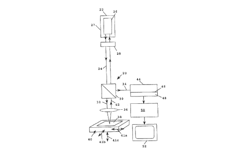
Microscope Construction. Figure 1 is a schematic
diagram of a high-resolution optical microscope 20 construc-
ted according to one embodiment of the invention. The
microscope generally includes a stable-resonator laser 22
designed to produce a coherent light beam 24. The laser,
which may be of conventional design, includes a resonator
cavity 26 within a housing 27, and internal optical and
circuit features (not shown).
One preferred type of laser is a low-power He-Ne gas
laser operating in two longitudinal modes, each of which is
linearly polarized. An internal linear polarizer blocks the
passage of one of the two modes, so that only a single
linearly polarized low-power beam is available externally.
B
206~2~2
One laser of this type which is suitable commercially avail-
able is a Uniphase Model 1101P He-Ne single-mode gas laser
(Uniphase, San Jose, CA). Where it is desired to perform
target mapping at target vibrations in the MHz range, as
described below, a semiconductor laser, such as are commer-
cially available, may be used.
In the present embodiment, where the laser output is
linearly polarized, the beam is passed through a half-wave
plate 28 which allows the direction of linear polarization
to be rotated in a plane perpendicular to the output beam.
This effect can also be achieved by rotating the laser
itself. Following the half-wave plate, the beam is split by
a polarization-dependent beam splitter 30 which passes the
component of linear polarization parallel to the plane of
incidence straight through, and deflects by 90~ light whose
linear polarization is normal to the plane of incidence.
The portion of the laser output beam which is passed through
the beam splitter is also referred to herein as an incident
beam, and is indicated at 32 in Figure 1. The portion of
the laser output beam which is deflected by the beam split-
ter is also referred to herein as a secondary beam, and is
indicated at 34 in the figure.
An adjustable-position objective lens 36 in the micro-
scope is used to focus beam 32 onto a target 38 whose fea-
tures are to be mapped, in accordance with the invention.The lens is preferably a 10 to 100 power lens having a
numerical aperture between about 0.6 and 1.2. The focused
beam preferably has a beam diameter of between about 0.5 and
2 microns at the focal point of the lens, and the depth of
focus of the beam is preferably between about 1-2 microns.
The lens is also referred to herein as means for focusing
the laser output beam onto a target.
The target is supported on a movable stage 40 designed
for moving the target in a manner which allows the focused
20S6202
-
light beam to "scan" the target. That is, the target is
moved in a systematic, preferably time-dependent manner in
the x-y plane (the plane normal to the beam axis) which
brings each region of the target to be viewed into the
focused beam. The stage is also designed for small-dis-
placement oscillation or slow displacement in the z direc-
tion, i.e., the direction of the beam.
In the embodiment shown, the stage is moved by x, y,
and z micrometer heads, indicated by arrows 41a, 41b, and
41c, respectively. These heads can be controlled by a DC
voltage input, according to standard operation.
Alternatively controlled movement of the stage can be
performed by piezoelectric transducers, such as indicated
also by arrows 41a, 41b, and 41c, which may be driven for
slow controlled movement in a selected x, y, or z direction
by a DC input, and which may be driven by an AC signal for
oscillation in a desired direction and at a selected fre-
quency. In one preferred operating mode, the target is
vibrated in the z direction by a piezoelectric transducer
(indicated by arrow 41a) at a selected frequency in the KHz-
MHz range. The amplitude of vibration is preferably less
than 100 nm. The purpose of the vibration is to avoid the
problem of 1/f DC power noise, by recording fluctuations in
laser power output on a high-frequency AC "carrier," as seen
below.
The stage and the movement effectors indicated by
arrows 41a, 41b, and 41c are also referred to herein, col-
lectively, as means for moving the focused beam relative to
the target in a defined pattern. It will be appreciated
that the moving means could alternatively include a movable
lens assembly for scanning the beam over the target in a
defined pattern, according to known lens assembly construc-
tion and operation.
20S6202
-
When the incident beam strikes the target, a coherent
reflected light beam 42 is reflected by the target back
along the path of the incident light beam. (The incident
and back reflected beams, which are coincident light beams,
are shown as separate lines in Figure 1 only for the sake of
clarity.) This back-reflected beam is transmitted by the
beam-splitter and reenters the optical resonator cavity of
the laser, as indicated in the figure. The light that
reenters the cavity interferes with the standing wave dis-
tribution of light in the cavity, and this interference,which depend on the phase of the back-reflected light,
changes the output intensity of the laser. The general
phenomenon of phase-modulated laser output has been reported
~King, Clunie).
The phase of the reflected light beam varies according to
displacements, along the beam axis, between the laser and
the region in the target at which reflection is produced.
These regions of reflection may correspond to reflecting
regions on the target surface, or they may correspond to
subsurface features, below a transparent surface, where a
change of index of refraction produces light reflection.
Such displacements can be measured in the picometer/nanome-
ter range, and more specifically in the range from about 1
picometer (10-12 meters) up to about one-fourth of the laser
beam wavelength, that is, up to about one hundred nanometers
(10-7 to 10-6 meters, nm). Even greater resolution, down to
about 0.1 picometer, is theoretically possible by limiting
laser fluctuation noise, detector noise, and apparatus
vibrational effects, as noted below.
The retroreflected light beam 42 which enters the laser
cavity is preferably only a small portion of the incident
beam, typically about 0.1% or less of the total incident-
beam power. This level is achieved, generally, when the
target gives non-specular reflection. For a target which
_ 20~S2~)2
gives specular reflection, the level of retroreflected light
can be reduced to a desired low level, in one approach, by
tilting the plane of the target, so that the back reflected
light beam which enters the laser, i.e., the retroreflected
light beam, represents diffuse reflection from the surface.
Alternatively, the back reflected light beam may be passed
through a half-wave plate and beam-splitter or through a
neutral density filter before reaching the laser, to produce
the desired power attenuation in the retroreflected beam.
The secondary beam from the laser is directed onto a
photodetector 44 designed to measure the power of the laser
output beam, by measuring the power of the deflected, secon-
dary beam. The photodetector includes a silicon photodiode
46 which is designed to measure light intensity. One suit-
able type of photodiode is an EG&G SGD 100-A silicon photo-
diode.
The photodiode is connected to an operational amplifier
48 in the photodetector which outputs a DC component voltage
which is linearly proportional to the power of the light
beam detected by the photodiode. The operational amplifier
characteristics are such that the voltage signal output
which is typically obtained is in the microvolt/millivolt
range. The photodetector is also referred to herein as
means for measuring the power output of the laser output
signal.
The microscope also includes a processing unit 50 for
converting position-dependent changes in the power output
measured at the photodetector, as the beam is scanned over
the target, to position-dependent displacement information.
To this end, the unit records the laser power (photodetector
voltage) as the focused laser beam is scanned over the
target, associates each measured power with the correspond-
ing region of the target which produced that power, then
assigns that target region a given displacement value,
206~02
according to the measured laser power. From this data, a
displacement map of reflecting regions of the target is
constructed, for display at a suitable display device 52 in
the microscope.
The operation of the unit 50 will be described below
with reference to Figure 9. As will be seen, the microscope
can be operated in a mode in which both displacement and
reflectance maps of the target can be constructed from the
laser power output information which is recorded at unit 50.
Figure 2 illustrates a microscope 54 constructed ac-
cording to a second embodiment of the invention. The micro-
scope includes a laser 56 having a cavity 58, for producing
a coherent output beam 60, and an adjustable-position lens
62 for focusing the beam on a target 64, carried on a mov-
able stage 66. The laser, lens, and stage components are
similar to those described above. A back-reflected light
beam 68 from the target is directed into the laser cavity,
to modulate laser power output as described above.
Microscope 54 differs from microscope 20 in that the
power output of the laser is measured directly from the
laser cavity. To this end, a photodetector 70 is positioned
behind the rear of the cavity, as shown, for measuring the
intensity of light leaking through a mirror 72 at the rear
of the cavity. The photodetector is also referred to herein
as means for measuring the power output of the laser.
The photodetector signal is amplified by an amplifier
74, and the amplified signal is passed to a processing unit
76 operable to convert position-dependent changes in laser
output, as the focused laser beam is scanned over the sur-
face, to position-dependent displacements of the reflecting
regions of the target, as described above. A displacement
map of target reflecting regions constructed from this data
may be displayed on a display device 78.
2066202
Figure 3 shows a fragmentary portion of a photodetector
80 which may be used in either of the above microscope
embodiments, for measuring power or intensity characteris-
tics of different regions of the laser output beam. The
detector has a grid or matrix of photodetector elements,
such as elements 82, which collectively define a detecting
surface 84 corresponding approximately to the area of the
output laser beam being detected. It will be appreciated
that the grid of detector elements can detect power varia-
tions within the cross-section of the beam, if desired.
Surface Mapping Resolution. Figure 4 illustrates the
ability of the microscope of the invention to detect surface
displacements in the direction normal to the surface. The
target here is attached to a commercially available piezo-
electric transducer (PZT) having a response of about 4.4 nmdisplacement/V. A stiff paper card was attached to the
surface of the transducer to serve as the vibrating target
surface. Voltages from a sine-wave oscillator (10 Hz to 20
kHz) or the synchronized sweep frequency output from an
audio spectrum analyzer (Hewlett-Packard 3580A) were used to
drive the transducer directly or through an amplifier for
the larger motional amplitude ranges.
The PZT vibration amplitude is shown at the left axis
in Figure 4, and the corresponding power output in voltage
units, along the right axis. For each voltage applied to
the transducer the frequency was swept or varied from 200Hz
to 2.2kHz. The flatness of the traces indicates the flat
response of the piezoelectric over the range of driving
frequency.
It can be appreciated from the spectra shown in Figure
4 that the amplitude of the measured signals is linearly
related to the amplitude of the transducer vibrations. For
example, with reference to the two spectra at the top in
Figure 4, a tenfold increase in vibration amplitude (from 10
- 2066202
to 100 nm) corresponds to an approximately ten-fold increase
in detected laser output measured as a voltage; similarly, a
100-fold increase in vibration amplitude yields an approxi-
mately 100-fold increase in measured voltage. The noise in
the spectra for vibration amplitudes below 1 nm is due to
background electronic noise and random laser light beam
output variations. Similar results were obtained when the
target surface was a transducer covered with brushed steel,
plastic, and mylar.
The signal-to-noise ratio as monitored by the output of
the operational amplifier is due to laser-light intensity
fluctuations and electronic noise in the photodetector. The
exact noise voltage at the output of the current-to-voltage
electronics depends on the specific laser's amplitude fluc-
tuations, the detector and its associate circuitry, and on
the bandwidth of the measurement. For the bandwidth of the
circuit used, the noise voltage was 2 microvolts, giving a
signal-to-noise ratio of at least 40 dB.
In the method described above, displacement measure-
ments down to the 10 picometer range have been made. Thelimiting noise in the apparatus is due predominantly to
laser amplitude fluctuations, which in theory can be reduced
by up to two orders of magnitude. It is also noted that
detector noise levels down to 10-2 pm/~Hz)~'/Z have been
reported (Rugar et al.). Thus, assuming that mechanical
vibrations in the microscope can be reduced sufficiently,
the microscope should be able to detect position-dependent
surface displacements down to the 0.1-1 picometer range,
particularly by employing phase-lock or time-averaging
signal-to-noise improvement techniques.
The range of linearity with respect to amplitude can be
determined by keeping the frequency constant as the amplit-
ude is varied and plotting the power output (voltage) vs.
amplitude as in Figure 5. The linear relationship holds
- 20662~2
14
over a range of vibration amplitudes extending below about
one quarter of the incident light's wavelength. For vibra-
tion amplitudes greater than this upper limit, the relation-
ship becomes non-linear. However, as seen below, the rela-
tionship between vibration amplitude and measured laserpower output in the high-amplitude range is still predic-
table, and therefore useful in determining large-amplitude
displacements from the measured power output fluctuations of
the laser. For a He-Ne laser, the wavelength of emitted
light is 632 nanometers; thus, the range of linearity (ta-
king background noise into consideration) extends up to
about 150 nm.
Figure 6 is a theory parameter diagram of an experimen-
tal configuration used for measuring laser power output as a
function of displacement of a piezoelectric transducer (PZT)
88. Here Lc represents the length of the laser cavity 90,
defined by the two mirrors 92 and 94, and L represents the
distance between mirror 94 and a reflecting surface 96
carried on the PZT. Experimentally, the PZT was placed 20
cm from the laser exit port, and was driven by a DC signal
from a PZT high-voltage amplifier, or a 40 Hz AC sine wave
signal coupled to the amplifier. A silicon photodetector
(not shown) was operated in the photovoltaic mode so that
its voltage output was linearly proportional to the light
intensity input. The detector was positioned at the rear of
the laser head where a hole had been drilled to allow light
to escape from the approximately 99% reflecting back mirror.
The voltage signal from the photodetector was sent either
directly to an x-y recorder for plotting of the laser inten-
sity DC variation or to the recorder via a phase sensitivelock-in amplifier for plotting the magnitude of the AC
variation.
In a first study, the surface of the PZT was moved
slowly towards the laser (i.e. L decreased) and the output
- 206~2~2
of the photodetector was observed. The voltage output was a
DC signal with sinusoidal variation. The sinusoid went
through one period as the PZT moved one half-wavelength of
the laser light (316.4 nm). This behavior was observed for
three different surfaces: the polished surface of a silicon
chip, the rough backside of that chip, and the brushed
stainless steel surface of the PZT. The amplitudes of the
sinusoid as a percentage of the total signal from the photo-
detector were 47%, 1.3% and 0.3% respectively, for the three
surfaces.
In a second study, the PZT was oscillated about a
distance L with a fixed amplitude and frequency while L was
slowly decreased. The output of the amplifier, at the
oscillation frequency of the PZT t40 Hz) showed a sinusoidal
variation with full period corresponding to movement of the
PZT of a half-wavelength toward the laser. For the above-
mentioned three surfaces, the signal strengths as a per-
centage of the average signal from the PD were 13%, 0.13%,
and 0.25%, respectively, and 0.04% for the surface of a
stiff paper card.
In a third study, the amplitude of the oscillation over
a range of approximately 3 wavelengths (1.9 ~m) was varied,
at a fixed frequency and fixed L. The amplitude of the
signal from the amplifier, as a function of PZT vibration
amplitude is shown in light line in Figure 7. The response
amplitude shows a Bessel function behavior (solid line), as
predicted from laser resonant cavity analysis carried out by
the inventors (not shown).
Surface Reflectance Effects. As indicated above, a
variety of surfaces having different roughnesses and reflec-
tances were examined for displacement effects using the
microscope of the invention. One interesting finding is
that even surfaces with high surface roughness, such as a
file card, which may have a surface roughness corresponding
20G6~02
-
16
to several wavelengths, give measurable displacement effects
in the nm or lower range.
One explanation of this phenomenon is that the reson-
ance modulation effect due to the phase of back reflected
light is responsive to a weighted average of the wavelets
produced by reflection from othe various reflecting planes
in the target region. The phenomenon represents an impor-
tant aspect of the invention, since it allows for high-
resolution displacement measurements on target surfaces with
a wide range of surface roughnesses.
The reflectance of a surface, does, however, effect the
amplitude of the laser output response to displacements at
the surface. In the third study reported above, it was
found that by placing calibrated neutral-density filters
between the laser output and the reflecting surface, the
peak signal varied as the square root of the reflectivity.
Thus, at least within a wide range of reflectivities,
the contribution of reflectance to the laser output level
can be approximated from some determinable function, such as
a function which approximates laser response as a square
root of reflectivity. This function in turn can be used to
determine reflectivity of a target surface, by determining
the amplitude of laser power response, over a quarter wave-
length (between a m~X; mllm and minimum power response).
Surface Mapping Method. Figure 8 shows a portion of a
target 100 which has been partitioned into a grid of re-
gions, such as regions 102, 104, which correspond in area
approximately to the size of the focused laser beam used in
ex~m;n;ng the target. Each region has a reflection surface
which is displaced some given distance, such as d1 in region
102, above a reference plane, indicated at 106. In addi-
tion, the reflectance of the target surface may vary from
region to region, as indicated by the different levels of
shading in the figure.
2066202
Figure 9 is a flow diagram of one operating mode of the
microscope, for use in mapping both surface displacements
and reflectance, such as in target 100. Initially, the
focused beam is placed at a region xl, y1, such as region
102, in the figure. The target stage is then shifted at
least 1/4 wavelength along the z axis until minimum and
m~x; m~m laser power levels are recorded. This shifting may
be effected by a DC input into an electrically driven micro-
meter head or piezoelectric transducer, or by a piezoelec-
tric transducer rapidly vibrating at a 1/4 wavelength ampli-
tude. As discussed above, the measured amplitude difference
at m;~;~um and m~xlmllm laser power outputs can be used to
determine the reflectance from that region, according to a
predetermined relationship between amplitude of power output
variation and reflectance. This difference value is stored
in a buffer, for later use in constructing a reflectance map
of the target and/or for correcting displacement measure-
ments for differences in surface reflectance.
The stage is now moved to an adjacent region, e.g.,
Xl,l, Yl, and the procedure for determining the reflectance
value at this new region is repeated, and the reflectance
value is stored in the above buffer. The procedure is
repeated until the entire target has been scanned. From the
reflectance values which are calculated from each region,
the processing unit in the microscope, such as unit 50 in
microscope 20, generates a target reflectance map.
For displacement measurements, the stage is preferably
oscillated at a selected frequency about a fixed distance ZO
from the laser, where the amplitude of oscillation is sub-
stantially less than the expected target displacements whichare to be measured. The stage is now moved in the x-y plane
to scan the focused beam over each region. At each region,
the laser power level is measured, and an appropriate cor-
rection for measured reflectance at that region is applied
2066~02
18
to determine displacement with respect to the reference
plane, such as plane 106 in Figure 8. The corrected dis-
placement value is stored in a buffer, as indicated.
From the displacement values which are calculated from
each region, the processing unit in the microscope, such as
unit 50 in microscope 20, generates a target displacement
map. The reflectance and displacements values determined
for each region can be combined into a single surface map.
It can be appreciated from the foregoing how various
advantages and features of the invention are met. The
microscope provides high resolution (down to the low picome-
ter range) in an optical system, and thus avoids special
sample coating and/or dehydration procedures required in
electron tunnelling or scAnn;ng electron microscopes. This
allows a variety of samples, such as living cells, to be
e~Am;ned at high resolution.
The microscope is able to map surface displacement fea-
tures in a target having a reflecting surface, or subsurface
reflecting features in a target having a transparent sur-
face. In addition, and according to an important advantageof the invention, the microscope can make accurate distance
displacement measurements, in the picometer to nanometer
range, on surfaces whose roughness may encompass several
wavelengths variation. The microscope can obtain surface
(or subsurface) reflectance information, and this can be
used for constructing surface reflectance maps and correct
the displacement map data.
II. Optical Data Storage Device and Disc
Data-Storage Device. Figure 10 is a schematic view of
a portion of an optical data-storage apparatus or device 120
constructed according to another embodiment of the inven-
tion. The apparatus includes a stable-resonator laser 122
and an adjustable-focus objective lens 124 for focusing the
~ 19 ~ 2 o 6 6 2 o 2
lcse output bear, indicated at 126, onto the surface of a
cc:c-s;c:age disc 128
The focused beam preferably has a beam diame~er
cf be:ween about 0.5-2 micsons at the focal point of the
le~s, and the depth of focus of the beam is preferably
be.ween about 1-2 microns.
The construction and characteristics of the disc will
be des~ribed below. For present purposes, it ls noted that
the surface of the disc defines a plurality of data-storage
pos_tions, such as indicated at 130a, 130b, and 130c which
are located within concentric tracks 132a, 132b, 132c,
res?ectively, on the disc surface. At each data-storage
pcs~- o~, information is stored in the form of a reflective
-e~_~n ha~ing a selected displacement dista~ce above or
b~ a defined surface plane in the disc. The number of
different displacement distances is I = 2~, where I is greater
than 2 and preferably 3 to 8 or more. That is, the disc
stores I = 2N information states at each data-storage position
The disc is mounted on rotary motor 134 in the device
2G f~- rota ion, at a selected speed about the disc axis,
i~.d.ca~ed at 136, according to conventional disc drive
cc~.s~ruction.
An optical assembly 138 in the device is designed for
sh_fting the position of the focused beam to different
2~ selected tracks on the data disc. The assembly includes
lens 124 and pair of mirrors 140, 142 interposed between the
laser and lens for dlrect~ng the beam along a selected-
length horizontal path in the figure. Mirror 142 and lens
124 are carried on a lens carriage 144. ~he carriage is
shiftable, along a horizontal axis 134 in the figure, cor-
responding to a radial llne 135 on the surface of the disc,
to position the focused beam at selected tracks on the d~sc.
B
~ 20 2066~0 2
Shifting in the optical assembly is performed by a
motor 148 which is operably connected to the carriage, and
designed to shift the beam in selected increments, e.g.,
O.05 to 0.2 mm, corresponding to the radial spacing between
adjacent tracks on the disc. The increment of shifting is
also adjusted to preserve the phase relationship between the
output beam and the beam reflected from the disc back into
the laser. This is achieved by making the increments of
shifting, and therefore the spacing between adjacent tracks
on the disc, equal to an integral number of wavelengths of
the coherent laser beam. The position of the optical
assembly is under the control of a controller 150 which
instructs the motor to selected track positions on the disc,
according to well-known disc drive construction.
The power of the laser output is measured, as in the
Figure 2 microscope, by a photodetector 152 placed behind
the optical cavity of the laser, for receiving light from
the cavity through the rear mirror of the cavity and an
opening 154 formed in the rear of the housing. An amplifier
156 used to amplify the photodetector signal is connected to
a signal converter 158 which operates to convert time-depen-
dent amplitude changes in the voltage signal received from
the photodetector to binary data values at each of the
selected disc locations which was "read". The construction
and operation of the converter will be apparent to those
skilled in the art. The data information from the converter
is supplied to a data-handling device 159, such as a micro-
processor, which in turn can provide signals to controller
150 for accessing information from the disc.
In operation, the laser beam in the device is focused
onto the surface of a data disc, at a selected track in the
disc. As the disc rotates, each data-storage position is
seen by the laser beam as one of I = 2N surface displacements
above or below a defined reference plane. These surface
21 Vs 2 o 6 6 2 o 2
sr a_e;nents, in turn, produce a change ln the phase of the
1~5~.: re'lected back into the laser, causing a proportional
c'.a~.ge in the power output of the laser. The time-dependent
changes in power are converted by converter 15B to time-
5 depe~dent displacements read on the disc, and these areassociated with given addresses on the disc according to
known methods.
It will be appreciated that each data-storage position
represents a selected one of I = 2N information states. Since
lO the density of data-storage positions on the disc can be
ma~e subs~a-,.ially as high as in conventional discs (where 2
information ~tates only are stored at any storage posi-
t 5:1), the density of information on the disc, and the speed
w_:!~ w~ich information can be accessed from the disc is
~5 enhanced by a factor of up to N = log2 I.
Da~a-Storage Disc. Figure ll shows an enlarsed fra~-
me-. a y plan view of the surface of a data storaqe disc,
s ~ as d sc 128.
Tracks, such as tracks 132a, 132b, and 132c in
20 the disc are indicated by solid lines, and data-storage
pcs~.ions, such as positions 130a, 130b, and 130c, are
i~Aicated by dotted lines. The data-storage positions on
eac~ track are spaced from one another by a distance prefer-
ably between about 1 and 5 microns, and adjacent tracks have
25 a spacing between about 1 and 5 microns. The disc may be
further encoded with radial and disc-àngle information, for
determining disc position, and with track-position informa-
tion, to insure proper beam placement with respect to any
selected track, according to a conventional optical data
30 disc construction.
Figure 12 shows an enlarged fragmentary cross-sectional
view of disc 12B, taken generally alon~ line 12-12 in Figure
11, i.e., along track 132c. The disc ~ncludes a substrate
160 which may be any suitable, preferably rigid disc mate-
B
22 r 2 0 6 6 2 0 ~
rial, such as aluminum, glass, o~ the like. The substrates_pports a layer 162 whose outer surface defines the data-
storage locations on the disc. The thickness of the layer
defines the I = 2~ different displacement distances, or thick-
nesses corresponding to a selected one of I = 2N information6tate6 which can be stored at each data-storage location.
For purposes of simplicity, the discs illustrated
herein have 8 (2') defined displacement distances, which may
include the surface plane of layer 162 and 7 increasing
dep~hs below the surface, or 8 subsurface depths. The
different displacement distances Yd are
indicated by depth markings, such as markings 164, shown at
the left in Figure 12 and related figures which follow.
Thus, for example, the data stored at position 130c cor-
responds to a depth 5d, and the data stored at position130c', to a depth 7d.
Figlres 13A-13F shows one method of forming a disc 170
(Figu-e 13F) of the type described. Initially a substrate
172 is coated with an etchable layer 174, such as a silicon
layer, using known coating methods. Layer 174, which has a
preferred thickness of at least 2 microns, is coated with a
photoresist coat 176, for example, by spin coating to a
desired thickness, for example, 1-5 microns. Depth markings
in the layer, such as markings 164, are indicated at 164 in
the figures.
The coated disc ~s covered with a mask 178 whose open-
ings, such as openings 180, correspond to the positions of
the data-storage ~ositions which are to have the greatest
depth, Id, wher~ I ~ 2~. The masked photoresist coat is
exposed to W light, producing exposed regions, Such as
regions 182 in the resist coat (Figure 13A), and these
regions are remo~ed by development (Figure 13B), according
to known photolithographic methods ~e.g., Thompson). The
disc surface is then plasma etched for a selected period
B
~ 2 0 6 6 2 0 ~
_ 23
sufficient to etch the uncovered regions of layer 174 to a
depth d, corresponding to the distance between the outer
surface of layer 174 and the first depth marking.
The disc is then covered with a second mask 184 whose
S openings, such as openings 186, correspond to the positions
of the data-storage positions which are to have the next-
greatest depth (I-l)d (Figure 13D). The masked photoresist
coat is exposed to W light, these regions are removed by
development, and the coated substrate is plasma etched under
the previously selected conditions. This second plasma etch
step is effective to etch the just-uncovered regions of
layer 174 to a selected depth d, and the already-uncovered
regions to a depth approximately equal to 2d (Figure 13E).
With each repeated cycle, new regions of the layer are
uncovered and etched to a depth d, and previously uncovered
regions are etched an additional increment d in depth.
After I = 2N cycles, e.g., 8 cycles, all of the data-storage
positions have been etched to a selected depth, and the
photoresist layer is removed by stripping. As seen, the
resulting disc 170 is composed of an underlying substrate
and an outer layer definin~ Plural data-storage positions,
each with a selected one of I = 2N depths below the surface of
the layer.
Figures 14A-14B illustrate another method for forming a
data-storage disc 190 (Figure 14E) of the type described
above. Here a substrate 192 having an etchable layer 194 is
coated with a suitable photoresist layer 196, as above. The
resist layer is exposed to W light through a mask 198 whose
openings, such as openings 200, correspond to the data-
storage posltions which are to have the greatest depth, Id.
The light-exposed regions, such as regions 202, are removed
by development (Figure 14A), as above, and the disc is
chemical-etched or plasma-etched until the uncovered regions
of layer are etched to a selected depth Id (Figure 14B).
~ 20~620 2
24
The substrate is then stripped, coated with a second
coat 203, and this coat is exposed to W, using a second
mask 204 whose openings, such as openings 206, correspond to
the data-storage positions which are to have the next-great-
est, (I -1) d depth. The light-exposed regions, such as
regions 208, are removed by development and the disc is
chemical-etched or plasma-etched until the uncovered regions
of layer are etched to a selected depth of ( I-l ) d (Figure
14D).
With each step, a new pattern of data-storage positions
with progressively shallower etch regions is created, until
after I z 2N steps, a desired disc 190 composed of an underlying
substrate and an outer layer defining plural data-storage
positions, each with a selected one of I = 2~ depths below the
surface of the layer, is formed (Figure 14E).
Figures 15A-15D illustrate a method of forming a disc
210 (Figure 15D), based on the ability to control the depth
of removal of material from a photoresist coat, according to
the dose or radiation applied to the coat. Figure 16 shows
a plot of coat thickness remaining after development in a
positive-tone electron-beam resist coat, as a function of
total e-beam dose (in microcoul/cm2) applied to the coat
(plot from Thompkins, p. 105). As seen, the thickness
remaining in the coat after development is a well-defined
linear function of log dose, up to a saturation dose of
about 10l2 microcoul/cm2.
In preparing the disc, a substrate 112 is coated with a
positive-tone e-beam resist coat 115 (Thompkins) having a
preferred thickness of 2 or more microns. The resist layer
is then covered with a mask 214 whose openings, such as
openings 216, correspond to the data-storage positions which
are to have the greatest depth, and the coat is irradiated
with an electron beam (3-beam) for a period corresponding to
a desired depth of coat removal, i.e., corresponding to a
B
2s -206620 ~
selected dose. The effective irradiation depth is indicated
in coat 215 by shaded regions, such as regions 218, in
Figure 15A.
The first mask is then replaced with second mask 220
whose open$ngs, such as openings 222, correspond to the
data-storage positions which are to have the next-greatest
depth. The coat is now irradiated with an e-beam for a
period corresponding to the new selected depth of coat
removal, as indicated by regions 224 in Figure 15B.
This procedure is _repeated for data-storage positions
at each of ~~ ~l~t~ I = 2N depths, as shown in Figure 15C.
An~r ~lI= 2N irradiation steps, the irradiated coat is
developed to remove cavities in the coat cPrresponding in
depth to the selected irradiation doses, as shown in Figure
15C. After baking, to remove developing solvent from the
resist coat, the coat may be covered with a transparent
protective coat.
Figures 17A-17C illustrate a method of forming a data
storage disc 226 in which the regions of reflection in a
disc surface are provided by changes in the index of refrac-
tion at selected data-storage positions and selected depths
within a unlform-thickness layer. The disc shown in the
figures is composed of a substrate 228 coated with a layer
230, preferably about 2 microns thick. Layer 230 is formed
of a transparent polymer, such as polyethylene, whose index
of refraction can be selectively varied, in localized re-
gions of the layer, according to the degree of polymeriza-
tion at the localized regions.
Layer 230 is initially covered with a mask 234 whose
openings, such as openings 236, correspond to the data-
storage positions which are to have the greatest depth Id,
and the coat is irradiated with an e-beam whose energy is
calibrated to penetrate the layer to a depth I d, producing a
localized change in index of refraction at that depth. The
B
- 206620 ~ '
26
area of locali2ed change in index of refraction is shown by
solid line, such as line 238, at the bottom of an irradiated
resion, such as region 240.
The first mask is then replaced by a second mask 242
whose openings correspond to the data-storage positions
where index of refraction changes are to have the next-
greatest depth ( I -1 ) d. The layer is now irradiated with an
e-beam whose energy is calibrated to penetrate the layer to
the next-up selected depth, producing index of refraction
changes at that depth at the mask open positions, as shown
in Figure 17B. These steps are repeated until index of
refraction changes at each of ~ I = 2N depths is achieved
(Figure 17C).
This data storage disc can be con-
structed to include two or more transparent layers in astacked configuration, as illustrated in Figure 18. Here a
stacked-disc device 246 is composed of a substrate 248 and a
series of stacked layers, such as layers 250, 252, and 254,
each constructed according to one of the single-layer em-
bodiments described above. That is, each layer, such aslayer 254, has a surface region 256 which defines a plura-
lity of data-storage positions, such as positions 260, and
data is stored at each region in the form of a depth (or
height) which is a selected ~ I = 2~ displacement distances
below (or above) the surface plane of the layer. Each layer
has a preferred thickness of between about 10-50 microns,
and the disc may contain up to several hundred layers.
In a data-storage device which uses a multi-layer disc
of this type, the plane of focus of the coherent l~ght beam
is shifted for "reading" a selected layer by suitable lens
shifting means.
As an example of the increased data-storage density
which can be achieved in the stacked disc, the adjustable
position objective lens will be assumed to be a lOOX micro-
B
2U662~2
scope objective lens having a NA value of 0.6. This lenshas a focal plane depth of 10~. Such an objective will
distinguish layers of holes spaced 20~ apart. A medium
having an index of refraction of 0.01 would provide 0.1%
retroreflected light intensity. If 2mm of useful depth
is available (this will depend on the actual material
used), 1000 separate layers could be formed.
Although the invention has been described with
respect to particular embodiments and applications, it
will be apparent to one skilled in the art how the method
and apparatus of the invention can be modified or adapted
to a variety of other applications.