Note: Descriptions are shown in the official language in which they were submitted.
SYSTEM FOlR T~ ~X(:~HANGE OF DAT~ BETWEEN AN ELECIlRONIC
OBJE~ ~OUPLE~D TQ A TRANSF13R DE~VIC~ WITH l:~IST~NCI DATA Bll
R~TES, INSERTABLE OBJE~ AND ~RRESPONDING TRANSFER
DE~lOE
The field of the invention is that of systems ~or the exchaslge Df data
between two elements capable of being coupled together.
More specifically, the system OI the invention hnds application in the
exchange of data between at least one movable, insertable electronic object and at
least one trans~er device wherein:
- ~aid speciSc transfer device comprises means for the transfer o~ data into
and/or out of the memory of the insertable object;
- said insertable object9 hereinafter called a "sma~ inser~able object"
comprises an elec~ronic memoly associated with an access circuit and coupling
10means ~ccessl~le f rom the exterior of thc insertable object enabling the temp~ary
coupling9 by any means, of said insertable obje~t with said transfer objec~.
In the sense used isl relation to the present invention, t}~e coupling OI the
insertable object with the transfer device can be done not only by the total or
partial physical introduction of the insertable object into the transfer device bu~ also
by the simple placing of one against the other or, ~gain, by any other type of
physical arrangement enabling the exchange of data between them.
For example, the system according to the invention can be applied to ~he
exchange of data between a microcompu~er and an electronic element that can be
inserted into the disk drive of the n~icrocDmputer9 or into a memo2y card reader.
This situation corresponds nota~ly to the ~eachings of the prior patent
documents EP-A-0 373 411, US 4 701 601 and US 4 791 283.
0~l~e pa~ene d~ument P-A 0 373 411 published on 20th June 1990 relates
o an arte~ct of an element of a mngnetic stnp card, diskette or cassene type
capable o~ l~eing înser~ed in 8 data-processing mac~ine such as a computer or ~
microcomputer. According to this documenl, the insertable element is fitted out
with a processor, a data and/or program memo~y, and an inter~aee emulating the
means of communication used by a s~andard iDserta~le dement to co~lmicate
with the da~ proccssing equipment. The pr~essor mskes it possl~le to ea~y out
Dperations of coding and/or de&od~ and en~tiDg and/or declyptin~g message
signatures or access controls ~vhich are, for example, the conditions ~or the use of
a microcompueer. One of the ~ntal elemen~. of this ~pe of system is the elecsrical
supply~ of ~he 1nter~ace of the ~nsertable clemen~ According to ~Ihis document~ the
power source. may be constituted by a celJ or, again, by a generator acti~rated by the
movement of inser~ion of the insertable clement into the data processing
cquipment.
, ~ `' The document US 4 701601 delivered on 20th October 1987 describes the
general principle of a microprocessor-based porlable bank transaction card
~; cormprising, da~a processing peans and means to ~mulate a magnetic strip so that it
can be compatible with bank tcrminals for the reading of rnagnetic strip cards. This
patent mentions the problems of thc availabili~r of a source of power sufflcient ~o
~upply the card, no~ably means ~or the emulation of a magnetic s~rip (CDL 5,1.64-
67) and proposes the use of solar panels for recharging an accumulator in
minirnizing the emulation periods (col. 7,11.31 to 54).
'\ ( The US patent document 4 791 283 delivered on 13th December 1988 also
relates to a microprocessor-based portable banlc card comprising data processingmeans and means to emullate a magnetic strip. More specifically, i~ descnbes a
possible conf1guration ~nd geometry of circuits ~o make means to generate a
magnetic field throughout practically the eDtire length of a card~ enabling ~he
ernulation of ~ach bin~ry clement (bit) of informagion ~o be ~ansmined. The
electrical supply to the circuits is done by an external energy source (col. 4~ II.29-
3~?.
These two pri~r ~rt documeJIts relate speci~ lly ~o the field of bank cardsO
l'hey disclose no means D~ configura~i3n of the data exchanged between the card
- . . .:
2~6~
and the transaction tern~nal, and do not sa~isfactorily Jesolve ~he problem of
~upplying the microprocessor card with elec~ical power.
These problems are, however, de~s~ve o~es.
Generally speaking, ~ able or inserta~le object such as a l'smart"
dis~ette or mcmoly card, namely pro~ided with a~ least oDe electronic memo2y
associated with access circuits ~s characterized, firstly, by its mdependence aDd,
secondly, by its processing capacity.
As regards the process~g of ~he exchanged data, one of the problems that
arises idates to the compat~ q of the da~a bit ~ates among the processing means
0 of the transfer device, thc coupling means and ~he circuits providing access to the
electronic memory of the insertable object. More specifically, notably in the case
of magnetic coup]ing means such as those used by the exchange of data between a
diskcttc and the disk drive of a microcomputer, the bit rate is standard~d, typically
at a value of 250 to 500 Kbits per second.
The reception or transmission of data elements at 1hese bit sates calls for
a corresponding processing capacity ~n the part of the circuits providing access to
the ~lectronic memoly of the insertab1e object. The telm "circuits providing access
to the mem~' here as well as further below implies any means eapsble of
managing access to said memory, including a D ~ieroprocessor or a microcontroller
(a microprocessor incorporating inter~ace elements such as an UART or universal
asynchronous receiver transmitter (asynchronous serializer/~esenali~er) and/or
memo~y of its own).
Now, in the current state of art, it is dif~lcult to meet this requirement
under commercially and technically acceptable conditions.
It is true that there are compact processors capable of being mounted in
a ~at element such as a memo~y sard or diskette, and capable of managing data
elemerlts at these flow rates. }Iowe~er, these processors consume a quanti~ of
p~wer ehat exceeds the capaci~r of the best per~orming cells no~r available at
~easonable cos~ (for example Li-Mg cells), for a satisfactoIy penod of use in the
desired application.
2 ~
~ ulthermore, there do ~t micrc~processors wh;ch are more cconomical
sn ~erms of power consumed, but their performance characte~istics ars not sufficient
to pr~ss the data bit rates consider~.
Finally7 we may en~isage a ~pecific microprocessor conffguratioll adapted
to thesc constraints, but the cost ~ desi~g such componer~ d tbe relative~
small size of the mar~et cnvisaged ~or t~esc specific microprocessors makes
approach unprofitable ~n prindple.
Furthermore, the magnetic coupling means used in ~he disk dri~es of
microcomputers generally include specific data codiDg means ~nth wh;ch they haYeto bc compatible. Thus, ~he microcomputers of ~he ~pe marketed by IBM used a
coding called MF~5 (modified ~equen~y modulation), and those marketed by the
Apple firm used a coding called GGR (group coded recordillg). The ~M, GC~
or equivalent codings are essentially aimed at coding informat;on elements in a
i~orm sdapted to the constraints ~f magnetic transmission, and any system of data
exchange ~n this context should take ~ccount of these constraints.
The invention is aimed ~t resolv~ng these differenS problems.
More precisely, the a;m of the inYention is to pr~vide a s~rstem of data
exchange between a smart insertable object and a tranfer de~ice, said system
enabling the use, in the insertable objec~, of componentsworldng at a lower bit rate
than the coupling means through which said illsertable object communicates with
said transfer object.
Another a;m of the invention, adapted to one of its preferred embodi-
ments, is to enable the maldng Qf smart compact diskettes, compatible with the
standardi~ed magnetie disk dr.ives with which microcompu~ers, in particular, can ~e
iGt~ed out, in using commonly available dectronic components ~hat consume li~tlepower, despite the low capaci~r of componen~s of this type in processing high b;t
rates.
These aims, as w~l as o~hers that shall appear here below, are ~c}lieved
according to the inven~ion by means of a system ~or the exchange o~ data between
.
,: , , .
.
... . , , . ' ,
2~$~46~
at leas~ onc m~able, inser~able electronic object and at le~s~ one transfer device,
- ~aid inserlab]e object wmprising aII elec~onic memo~y associaled ~th
an access c~rcuit and coupling means enabliDg the tempalra~y ~oupling of said
insertable object with said ~ans~er dc~
- ~d transfer device cc)mprising means for the trans~er of data into snd/or
out of ~be memo~y of the hserts~le object;
- said insertable object emulating a magnetic ~ecording supportwith respect
to a magne~ic read and/or write head of the transfer dcvice, the data exchange bit
rate of the transfer de~nce being greater than that of the access circuit of the memo~y of the inse~able object,
wherein said srstem comprises means to limit the b;t ~ate of useful data in the
app~rent bit rate of data entering and/or leaving the tsansfer device, so that it is
~mpatible wJth the bit rate 1eaving and/or entering ~he access circuit of the
memory of the insert~ble object.
LT1 th;s way, not only is the exchange of data between the transfer device
and the insertable object made possl~le, but also a substantial par~ OI the processing
capaci~r of rate adaptation can be tran~fe~red into the trans~er devîce, ~ shall be
seen further ~low, thus maldng it possible to cconornize on the processing capacit~
of the insertable object4
;!o Ac ording to a pre~erred charactelistic nf the im~ention, said means to limit
the bit rate of useful data elements include means ~o insert padding informationinto the flow of data entering andlor leaving the ~ransfer de~ice.
Advantageous~, said mesns to insert the padding information include
means for ~he redlmdant coding and/or n times ~n~2) replication of at least certain
of said useful data, in the ~low of data en~erin~ and/or leaving lhe transfer device.
Pre~erably, in the channel for the exchange of da~a in ~he direction going
f~om said transfer device towards said inse~ble device9 said means f~ the
leplicatioTl of at least some of the useful data cooperating wi~h specific coding
means of the MFM9 GCR oJ equavalent ~ype, p~sitioned downline f~om said
~eplication mean~, said leplication an~ ~M or equivalent coding means being
6 ~
located in the ~ansfer device.
In this case, advantageously, ~e eombina~ion o ~e data processing
operations by the replica~ion means and then the M~ or equi~alent coding means
~es, for each bit c~f useful in~ormat;on, 8 ~eque~ce ~ data within whiclh l~here~lternate senes of ones and zeros according to a fi~t patterIl for a useful bit equal
lo zero, a~d according to a ~ecoDd pattern for a useful ~it equal ~o orle,
wberein ~aid irssertable bit ~mprLses pat~em discrimination means d;scnminating
betwcen lhe first and second patterns so as to reco~er each of the successive useful
bits in the data flOw ente~ing said insertable objec~
It is advantageously possll~le to choose a method hr ~e insertion of
padding clements leading, after MFM, GCR or cquivalent coding by tho transfer
device, to periodic predetermined patterns displaying changes in ss~te according to
A first periodicity for ~he first pattern and accDrding to a second periodicity,difEerent ~om the first periodicity, for the second pattern. In this way, the
recognition of the patterns may be reduced to a simple ~equency discrimination.
To simplif~ the processing s3 stem i~ the insertable object, said f~equen~y
discnn~ination means may thus dircctly supply the series/paralle} converter
associated with a processor located in said insertable object, synchronized Wit~l the
frequency of periodic patter~l changin~g in the ffow of data ensering said insertable
object.
According to another advantageous characteristic, said useful data elements
are assembled in data streams comprising delimiters, before the processing
operations by said replication ~nd MFM or equivalent coding means, and said
delimiters pro ~ide ~or the locking of ~mchronization of said cir~ui~s providing access
to she memo~y o~ the insertable o~ject. ~hus, in ~e advantageous example whcre
~he circuits pro~iding a~ess to the memo~y comprise a microproeessor accessl~le
through a deserializer, it is the latter that ge~s ~nchronizçd with ~he delimiters. This
makes i~ possl~le to avoid resorting ~o means, generally costly in terms of power,
to synchronize the clocX signal of ~he processor of the insertable obJect wi~h the
3G data received from t~le trans~er d~ce, namely synchronizin~ means such as a
phase-lock l~p or equivalene device.
Preferab~y, in ~he channel for ~he e~chan~e of data in the direc~ion going
~om said insertable object to said ~ransfer device, said n~eans for the inser~ion of
padding data ineludle means to memorize pre-prepared sequences of bi~s and meansfor the ~rans~ission oP said pre-prepared ~equence~ as a funetion of u~eful datselements ~o be trsnsmitted. 5aid pre-preparcd ~uen~s of biLs are ob~ained9 for
e~ample9 ~om processing operations of replica~ion, ~ or equh~lent coding
and/or CRC eoding.
Preferably, the useful data elements are pro~rided ~te by ~yte, and said
means to snsert padding data insert a padding ~equence at the ms~nt of each
~eading of a new byte of usef~ data elements in the electronic memory of ~aid
inserta~le object.
Other features and advantages of the invention shall appear from the
following descnption of a preferred embodiment of the invention, gnJen by way ofa non-restrictive embodiment, and from the apperlded drawings, of which:
- Figure 1 gives a schematic v.iew of the main fimctional modules eoming
into play in the processing line of ~he data exchange system of the invention;
- Figure 2 illustrates a preferred embodiment of the system of figure 1,
using available components;
- Figure 3 illustrates the successive processing operations applied to useful
da~a to be transmit~ed ($CS) along the processing line in the tr~nsmission channel
~om the transfer de~ice to the processor Df the embodiment of figure 2.
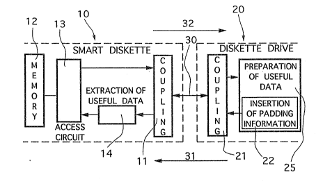
Figure 1 brings out the main functional modules coming in~o lplay in the
data exchange system of the invention.
The drawing of figure 1 shows the placing of an inser~able o~ject 10 in~o
commun;cation with a transfer device 20. The object 10 and the de~ice 20
communicate through their coupling means 11, 21. Preferably, these coupJing means
are magnetic cbupling means but the invention CaD 81so be transposed to other
2 ~
types of coupling means, ~or example c1ectromagne~iG, optical, capaeitiv~ means e~c.
~ the ~xample discussed here below, the transfer dleYice ~0 c~responds
to lhe standardized disk drive of a microcomputer, and the insertable object 1û is
a nsmart" diskette, n~me~ a dis~et~e lpro~ded ~th an elec~rorue memo~y 12
associated ~vith an access c~r~it 13 aDd compr~ing coupling means 11 emulating
a standard dis~ette with re~pect to th~ disk ~e 21).
l'he invention makes it pDssibie lO mee~ a tw~fold constraint:
~ pr~viding for the standard bit ~a~e prescr~bed for the flow of data 30
exchanged witb the disk drive (typically 250 to 500 Noits per second);
- using means for the processing of data in the smart disk 10 possessil~g a
limited processing capacity, and notably beinB incapable of processirlg any other
than A bit rate smaller than that of the data flow 30, owing to the limitations of the
circuit 13.
The coupling means 11, 21 mutually exchange a data flow 30, ha~ing an
apparent bit rate equal to the standard bit rate.
According to the invention, the apparen~ bit ra~e of the data flow 309
namely the number of bits per second really exchanged, is gr~ater than the bit rate
of useful data in ~e flow ~f daSa 30. This results from the ~act that the useful da~a
elements have undergone a plior processing operation by which padding irl~orma-
tion (~or example redundant, ~ver-abundant or non s;gnificant in~ormation) has
been added to the useful information to form the data ~ux 30.
Thus, in the channel for the exchange of data in the direction 31 goirlg
~om the disk drive 20 to the smart disk 1û, the disk drn1e has a module 22
comprising means ~o insert padding informa~ion into the data flow 30 coming out
of the disk dnve 20.
The data fl~w 30 entering ~he smart disk 10 should ~en be processed in
the module 14 for the extraction, therefrom, of the useful da~a which will be
exploited by the assembly formed by the elec~ronic memory 12 and i~ access
- circuits 13.
~igure 2 illus~rates a concrete prefe~Ted embodiment o the functional
:
drawing of figure 1.
The smart diskette 10 is built around 8 proce~sor 40, ~or -xample of the
class 6~ S marketed by MOTORC~I~ for example the 6~I005(~ orS again, the
68H005A6.
The processor M68HC05A6 is an ~bit prQcessor having the ~ollowing
resources:
- 4 Kby~es of ROM;
-176 bytes of RAM;
- 2 Kbytes of EEPROM;
0 ~ 1 clock circuit activated by an ex~ernal ~ystal 41;
- 1 paraDeVscries converter 42;
- 1 asynchronous series/parallel converter 43.
By using 8 2 MH~ Cl'yst8l 41, the consumption of the processor 40 should
be of the order of 3 rnilliamperes at 3 ~olts. At this ~equency, the processing speed
attained is abou~ 56% ~ the proc~ssing speed of a presently ~vailable chip card
fitted out with a MOTOROLA micropro~essor. These pe~formance characteristics
are sufficieD~ to perfoml, for example, DES type cryptography slgonthms, or again
key management algorithms, in logic access control spplications. Other t~pes
algorithms, both present and fature, and other typ~s of applications are naturally
compatible.
The electrical supply may be ~provided, for example, by a cell 44.
Advantageously, the cell used m~y be a lithium-manganese cell of the 2~25 ~type
5h = 2.5 mm; diameter - 20 mm; 3.0 V; 140 m~h) or of the ~4-30 type ~h - 3.0
mm; diameter = 24.5 mm; 3.0 V; ~70 mAh).
~ single 2~25 cell at 140 milliamperes/hour has an irldependent working
time of 35 hours at a current of 4 milliampeFes. This represeDts one year of
opera~ion at 5 minutes per day.
Th~ smart diskette 10 further ~ncludes magne~ic soulpling means 11 which
ma~r be consti~uted, ~or ~xample, by a simple coil, or again by ~evices of greater
sophistication su(~h as the one descn~ed in the patent dr~cumes~t US 4 7912~3
6 1
discussed here abo~e, ~r ag~ by any other appropnate device.
Between the micropr~ssor 40 and the c~upler 11, there is a ~equen~y
dis~atiDn module 49 in the data exchange ~hannel from the drive 20 t~ward
the diskette 10.
1~ the drive 20 - diskette 10 exchange c~annel, the useful da~a prepared by
th processing means 25 of the reader undcrgo a dual cascade processing:
~ a fisst processing 23 of coding by redundancy and/or by replication, bywhich each bit 0 or 1 of useful data is coded on n bits (n 2~;
- a coding 24 ~dapted go the ~ansmission by magnetic couplin~g, of the
MF~q (modified frequency modulation) CodiDg or other t~pe.
Through this cascade coding, thc bit raSe of data elements transmitted ~o
the magnetic couplers 21, 11 may attain the prescnbed standard values (for example
S00 Kbiss per second) with useful data elements at a bit rate that is 2n timcs
smaller~
Any other coding that achieves the same resull may also be implemensed.
H~wever, the coding ~ewmmended hereill seems to be the optimum one at presenS,
for the following reasons:
- the MF~ (or equivalent) coding 24, typical of a transmission by magrletic
coupling, makes it possible to optimize She transn~ssion o~ info~nation elements~om the coupler 21 to the coupler 11;
~ the ~edundancy coding 23 increases the apparent bit rate of data (which,
moreover, is subsequently doubled ~ ~he MFM coding 24) in relation to the usefuldata bit rate;
- the coding 23 can finally be chosen so as to simplif~ the decoding done
an the smart dis~ette 10.
An exemplaTy implemelltation compatible with these di~rent aims is
illustra$ed in figure 3.
Figure 3 illustrates the different codin~ steps carried out in ~he da~a
exchange chamlel 31 going from the disk drive 20 so the smart diskette lQ
'~e example talcen corresponds to ~he ltransmission of usefu1 data $CS,
~6~1
11
which ~ the hexadecimaJ representa~ion of the following l~
110001Q1
~ he first step consists in framinB ~his byte by delimiters, a~er having tulmed
the ~yte o~rer to place ~e least significa~t by~e at t:he head:
O ~ 0 1 0 ~ O 1
Start ~top
l'he ndundan~ coding d~ne m ~he module 23 is camed out according to
the folloYnng rule:
- each bit equal to O is coded in ~he ~orm 0101.
- each bit cqual to 1 is coded in thc form 1111.
Consequently, the byte $C5 between its ~vo delimiters STAR~(O) and
STOP(1) is coded in the ~orm of five successive bytes $5F $5F $55 $5F $FF 8S
shown in line 60 of figure 3.
The data bit rate is there~ore, in this ~se, multiplied by S ~ter the
imp]ementation of this coding 23.
lh~ data stream 60 ob~ined is ~hen subjected to ~e MFM coding of the
module 24.
The ~ coding is a standardized c~ing OI a ~awll t3 pe, used notably
to obtain access to 720 K disXettes. It is done according to the following ru1es:
- each data bit at 1 is coded in the i~onn ST ~S - Steady, identical to the
preceding bit; T = Transition: the reverse of the precedîng bit~;
- each data bit at 0 is coded in the fonn SS if the preceding data bit is 1
or TS if the presed;ng data bit is 0.
By application of these rules, the ~ansitions in the MFM data stream occur
a~ intervals of 4.6 tQ 8 ~S.
The se$ult thereof is that the continuous sequences of the lllIIlll ~pe
are eoded i~ the fonD of tr~nsitions ~ve~y 4 ILS (square waves at 125 KHz) and the
ûlO10101 sequences are: coded in the form of transitions eve~y 8 ~S (62.5 KHz).
Tho 1inc 61 of fif;ure 3 ~h~ws the si~fl1 ob~ained at ou~put Df the MFM
. , ~ . .
~6~ ~
12
codirlg module 24 f~om ~e useful data $C5.
The MF~ eDding is doDe in thc disk controD~r ~cuit of standard
microcompute~.
The u)mbination of u~dings done by ~e modules 23 snd 24 elegantly
simplifies ~e rcstitution of useful data clements in the di~klette 109 b3r means of a
dmple ~equent:y discriminatmg ci~cuit 49.
More specifically, after the casc~de coding, ea~ useful da~a bi~ is coded
in 1he .~.orm of a 3gua~e signal of 8 different ~equency depending on whether itcorresponds to a 1 or to a 0. The ~equeD~y discriminator 49 the~efore bas the
10function of detecting the instantaneous frequen~y of the signal 61 and gives, st
output, a signal 62 which is at ~he low level when R frequency of 62.~ KH[z is
detected (original useful bit = 0) and is at the high level when a frequency of 12
KHz is detected (original useful bit at 1).
At output of the frequen~y discriminator 49, the useful data 63 ære
therefore directly ~pven to the deserialiser 43 of the rnicroprocessor 40 of ~he srnart
diskette lQ This desenaliser 43 corresponds ~o the receiver half of the asynchro-
nous series/parallel converter (namely the UART or universal asynchrorlous
receiver transm;tter) of the microprocessor and rece*es the data elements between
STARTISTOP delimiters (start and stopbinary elemcnts) so that the data elements
20are assembled in bytes and given in a ~OT~I that is direct~ usablc by the micropro-
cessor 40.
The preparation of the data exchanged in the direction 32 (from the
diskette 10 to the disk drive 20) may be done by using a paralleVseries converter
42 intemal or external to the microprocessor 40, in cooperation with a pre-prepared
sequence memonzing zoDe 45.
So ~ ~o conform to the communication standard o~ the disk drives, the
data elements sent ~o the drive 20 should be consti~uted ~y ID address marks, data
address marl~s, data elements proper ~nd, finally, a ~yclic redundancy check word.
Owing to tbe relatively l~w processing speed of the processor 40, it may be
30necessary ~o increase the apparent bit rate of the data elements as compared wilh
.
~, ~
,
. . : : ' .
2~
13
the bit ~ate of useful data elements produced b~ the processor 40, in order to
con~orm to the ~ran~mission bit Tates of the magnetic couplers 11, ~1. In order to
~conomize on the processing capaci~ of the processor, the cocling of the useiFul da~a
clements pr~duccd by ~e proeessr)r 40 ~ not ~e place an real time but will
consis~ in sending precomputed sequences for each bit of usleful data provided.
More specifically, the ~ansmission procedu~e pres~nts the following steps:
- assembling of ~ytes of use~3l data, by way of illustration in sets of 8 (64
bits in ~11);
- pre computstion of CRC and its ~ coding;
- use of a program loop o~ ~he type ~h~wn in Table 1 (RomT~p) to
send I~ address msrks and data addr ss mark~. These markers may be pre-
computed, coded in M~M and memorized m the memoly zone 45, in conforming
to all the clock violatiQns cxpected by thc corltrol circuits of t~le drive ~0;
- the use of ~ program loop as shown in Tabie 2 ~EncodLoop) to send the
pre~mputed sequence, coded in MFM and memorized at 45 corresponding to
each of the useful bits of each of the eight l:~nes. The coding o~ usef 11 bits may be,
for example, c10se to ~he one ~ed ou~ in the modu1es 23, ~4;
- the emission of the GE~C pre-~omputed, MFM coded and memorized in
~e zone 450
Tables I and II represent program steps expressed in the programD~ing
language of the MOTOROLA microprocessor 6~HCa~.
These program steps are given by way of an ind;cation and can be used
directly by those sldDed in the art.
Ille instructiolts of ~he "run n s~ycles" ~pe are introduced to adjust the rate
~ emission of data elements to the w~rld~g rhythm of the paralleU~eries converter
43.
In table II, ~or each useful data ~it equal to I, the pattern sent is 001100I1.
For each bit equal to 0, the pattem sent is 00~1111.
In this e~ibodiment, the ooding o~ ~he useful data elemen~3 is theref~re
identical fc~r both d*ections of transmissio~
2~6~6~
14
However, the mvention also c~vers emb~diments w}le~e the codings are
distirlct. For cxample, it is possible to code each useful b;t orl lengthier sequences,
Tlotably ts facilitate the detecti~n n;ade by the fre~uen~y disc rimina~or circui~ 49 in
the ~Tansmission direction 31.
. ' - '. '~' :
.. .
:
,
2 ~
1~
TABLE 1
LDX #~1 ; number of by~es to be sent, minus 1
2 ~oml~Loop LDA 520,X ;4 ~ad ne~;t ~e ul ~;I~M
3 ST~ SERTOPAR ;4 load ~ serailizer 42
4 NOP ;2 wait 2 ~ycles
DECX ;3 run Ihrough ~ble aDd end of test
6 BPL Rom~Loop ;3 loop
TABLE 2
LI~X #8 ; Dumber of bytes to be ~en~
2 EIRA EncodStart
3 EncodLoop LDA #%OOOOIlll ;2 sent a padding panern for O101 (star~)
4 STA SERTOPAR ,4 load in setiali~er 42
; (oodage du bil O)
S NOP ,2 ~mit 2 ~ycles
BRSET O,TMP,ISTO ;5 tçst bit O of lMP
7 LDA ~c00001111 ;2 lf O, send pattern for O101
8 BRA as~ ;3
9 ISTO TSTA ;3 wait 3 cycles
LDA #~oO0110011 ;2 if 1, send pattern for 1111
11 GS10 STA SERTOPAR ,4 load i~ seriali~er 42
12; (coding og ~he bits 1~2,3,4,5 and 6 not shown)
; (coding of the bit 7)
13 NQP ;2 wait 2 ~ycles
14 B~SET 7,TMP,lS17 ;S lest bit 7 of TMP
IDA #~0001111 j2 if 0, send pattern for 0101
ï6 8RA GST7 ;3
17 lST7 TSTA ;3 w~it 3 cycles
18 EncodStan LDA ~YoO0110011 ;3 if 1, send pattern ~o~ 1111
19 GSrl ST~ SERTOPAR ;4 load in serializer 42
NOP NOP ;4 wait 4 cycles
21 LDA S80 1,X ;4 read next byte in the RAM
æ STA TMP ;2 ~torage in TMP
23 LD~ ~%001~0011 ^,2 send a padding pattern for 1111 (stop~
24 STA S~TOPAR ;4 loaa ;D Krializer 42
NOP NOP ;4 wait 4 qcles
26 DECX ,3 ~un through table and end of test
27 BPL EncodLoop ;3 loop