Note: Descriptions are shown in the official language in which they were submitted.
CA 02066552 2001-10-09
29903-93
1
APPARATUS FOR CONTACTLESS DATA AND ENERGY TRANSMISSION AND
METHOD FOR OPERATING SUCH AN APPARATUS
Specification:
The invention relates to an apparatus for
contactless data and energy transmission, including a
stationary part having means for transmitting and receiving
data, which are each respectively transmitted to a movable
part with the aid of a first pair of coils and having means
for generating energy, which is transmitted to the movable
part through a respective second pair of coils, the coils of
the stationary part are to be arbitrarily associated with
the coils of the movable part, and the data transmission
takes place from the movable part to the stationary part by
means of a load variation at whichever coil of the movable
part is not used for energy transmission, the coils of the
movable part are each followed by rectifier means, and the
rectifier means are each followed by a modulator. The
invention also relates to a method for operating the
apparatus.
Such an apparatus is described in European Patent
No. 0 466 949 Bl which became available to the public on
January 22, 1992, and in particular in Figs. 1 and 2 and the
description thereof.
That apparatus for contactless data and energy
transmission includes a stationary part (ST) having an
oscillator (OSC)
1
2066552
for contactless power transmission to a movable part (BT)
with the aid of a pair of coils (LlA, L2A; L1B, L2B), wherein
the oscillation of the oscillator (OSC) is split into a
reference oscillation and an information oscillation, and a
phase displacement with respect to the reference oscillation
is forced upon the information oscillation as a function of
the data (DT1) to be transmitted, the phase-displaced oscil-
lation is delivered to the movable part (BT) through a first
pair of coils (L1B, L2B and L1A, L2A, respectively) and the
oscillation voltage is delivered to the movable part (BT)
through a second pair of coils (L1A, L2A and L1B, L2B,
respectively), wherein in the movable part (BT) the transmit-
ted oscillations are delivered to a demodulator circuit
(DEMOD), which recovers the data from the phase displacement,
and a data transmission from the movable part (BT) to the
stationary part (ST) takes place by means of load variation.
The power transmission is accomplished with only the aid of a
pair of coils, and the data transmission from the movable
part to the stationary part is accomplished only by load
variation at the coil of the movable part that is not used
for power transmission.
Tn order to assure that the coils of the stationary part can
be associated arbitrarily with coils of the movable part to
form pairs of coils and thus to assure that energy or data
can be transmitted through each of the two coils, even if not
simultaneously, each of the two coils of the movable part is
associated not only with a rectifier circuit but also at
-2-
~~66~~2
least with the final control element of a voltage regulator
and moreover with at least one switch, which is capable of
varying the load on the pair of coils associated with it as a
function of its triggering and the resultant switch position.
It is also possible for each of the coils to be associated
with one voltage regulator and one variable load. In all
such cases, it must be assured by means of a logical linkage
that the amplitude modulator required for the data transmis-
sion from the movable part to the stationary part always
varies the load of the pair of coils that has no part in the
energy transmission, and has a voltage regulator or voltage
regulator final control element that is consequently not
active, or which does not have the voltage regulator connect-
ed to its output side.
If the coils of the movable part and the coils of the sta-
tionary part are intended to be arbitrarily couplable and
therefore a demodulator circuit having a circuit unit for
fixing the logic level of the signal is provided, then the
circuit unit can also recognize, in the same way as it fixes
the logic level, which of tha coils of the movable part the
reference oscillation is to be transmitted to and which of
the coils of the movable part the information oscillation,
which is variable in its phase relationship with the refer-
ence oscillation, is transmitted to. In such an apparatus
for contactless data and energy transmission, as a function
of a demodulator circuit signal containing the information, a
logic linkage fixes which coil of the movable part is used
-3--
20G6~~2
for data transmission from the movable part to the stationary
part and which coil is used for the energy transmission,
which assures that the data transmission from the movable
part to the stationary part is performed with the aid of the
coil of the movable part that is not being used for energy
transmission at that moment. In order to assure a continuous
energy supply to the movable part, the coil transmitting the
reference oscillation is followed by a voltage regulator, or
activates a voltage regulator connected to the output~side of
the coil, and at the coil of the movable part that transmits
the information oscillation, the data transmission from the
movable part to the stationary part varies the load as a
function of the data to be transmitted.
A disadvantage of the above-described configuration is that
one respective load capacitor is needed for each coil and for
each following rectifier, which requires a considerable
amount of space upon integration. Another disadvantage is
amplitude modulation feedback upon the supply branch result-
ing from whichever modulator is in operation at a given time.
It is accordingly an object of the invention to provide an
apparatus for contactless data and energy transmission and a
method for operating such an apparatus, which overcome the
hereinafore-mentioned disadvantages of the heretofore-known
methods and devices of this general type, which take the
smallest possible amount of surface area for the charge
-4-
2066~~~
capacitor in integration and which avoid the amplitude
modulation feedback.
With the foregoing and other objects in view there is provid-
ed, in accordance with the invention, an apparatus for
contactless data and energy transmission, comprising a
stationary part having means for transmitting and receiving
data and means for generating energy; a movable part having a
plurality of rectifier means each with at least one output
and modulators each being connected downstream of a respec-
tive one of the rectifier means; a first pair of coils
connected to the means for transmitting and receiving data in
the stationary part and to the rectifier means in the movable
part for transmitting data from the stationary part to the
movable part with the aid of the means fox transmitting and
receiving data; a second pair of coils connected to the means
for generating energy in the stationary part and to, the
rectifier means in the movable part for transmitting energy
from the stationary part to the movable part: the coils in
the stationary part being arbitrarily associated with the
coils in the movable part, and data being transmitted from
the movable part to the stationary part by a load variation
at which ever coil of the movable part not being used for
energy transmission: a charge capacitor, and controllable
semiconductor elements each having a load path connected
between the at least one output of a respective one of the
rectifier means and the charge capacitor at which an unregu-
lated operating voltage can be picked up, for delivering
-5-
2066~~~
output signals of the rectifier means to the charge eapaci-
tor.
In accordance with another feature of the invention, the at
least one output of each of the rectifier means is in the
form of first and second outputs; and each of the modulators
includes a first transistor having a control terminal and
having a load path through which the first and second outputs
of one of the rectifier means are connected to one another; a
second transistor having a control input and a load path, a
resistor connected to the load path of the second transistor
in a series circuit connected between operating voltage
terminals, the series circuit having a node point connected
to the control terminal of the first transistor; an opera-
tional amplifier having an output connected to the control
input of the second transistor, a negative input receiving a
reference voltage, and a positive input, a third transistor
having a control input and having a load path connected
between the positive input of the operational amplifier and
the first output of the one rectifier means, a fourth tran-
sistor having a load path and a control input, a second
resistor connected to the load path of the fourth transistor
in a series circuit between the positive input of the opera-
tional amplifier and the first output of the one rectifier
means; third and fourth resistors being connected in a series
circuit between the two inputs having a node point connected
to the positive input of the operational amplifier; a first
control input connected to the control terminal of the fourth
-6-
20~6~~~
transistor for receiving a data signal: and a second control
input connected to the control input of the third 'transistor
for receiving a signal fox disconnecting the modulator and
the rectifier from the charge capacitor.
In accordance with a further feature of the invention, there
is provided a capacitor connected between the two outputs of
the one rectifier means.
In accordance with an added feature of the invention, there
is provided a controllable current source connected between
the operating voltage terminals; and a current mirror having
an input side serially connected to the controllable current
source and an output side connected between the control input
of the first transistor and the second output of the one
rectifier.
In accordance with an additional feature of the invention,
the apparatus for contactless data and energy transmission is
part of a check-cashing card or chip key.
With the objects of the invention in view, there is also
provided a method for operating an apparatus for contactless
data and energy transmission, which comprises ascertaining
which coil is used for energy transmission during an initial-
izing time within the movable part, and thereupon disconnect-
ing the rectifier means and the modulator from the charge
~oss~~~
capacitor through the applicable controllable semiconductor
element.
one advantage of the invention is that in terms of circuitry
expense and complication, relatively modest means are,provid-
ed, which make it possible for whichever modulation bridge is
in operation at a given time to be disconnected from the
supply branch.
Other features which are considered as characteristic for the
invention are set forth in the appended claims.
Although the invention is illustrated and described herein as
embodied in an apparatus for contactless data and energy
transmission and a method for operating such an apparatus, it
is nevertheless not intended to be limited to the details
shown, since various modifications and structural changes may
be made therein without departing from the spirit of the
invention and within the scope and range of equivalents of
the claims.
The construction and method of operation of the invention,
however, together with additional objects and advantages
thereof will be best understood from the following descrip-
tion of specific embodiments when read in connection with the
accompanying drawings.
_g_
~0~6~52
Fig. 1 is a fragmentary block and schematic circuit diagram
of a basic configuration of an apparatus for contactless data
and energy transmission accord:lng to the invention;
Fig. 2 is a schematic circuit diagram of a modulator circuit
of Fig. 1, according to the invention; and
Fig. 3 is a fragmentary schematic circuit diagram of an
expansion of the modulator circuit shown in Fig. 2.
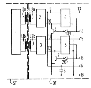
Referring now to the figures of the drawing in detail and
first, particularly, to Fig. 1 thereof, there are seen
details of a stationary part ST, which has first and second
'transmission coils Lla, Llb and one function unit 1. The
function unit 1 includes all of the essential devices for
transmitting energy and for transmitting and receiving data.
A movable part BT which is also shown in fragmentary form,
has first and second coils L2a, L2b. Therefore, the coils
Lla, L2a may be considered a first pair of coils and the
coils Llb, L2b may be considered a second pair of coils. Of
course, the coils Llb, L2b may be the first pair and the
coils Lla, L2a may be the second pair. The first coil L2a is
connected to a first rectifier unit 2. The rectifier unit 2
has first and second outputs 9, 10, which in turn are con-
nected to a modulator unit 4. The modulator unit 4 has
control inputs 13 and 14. The second coil L2b is also
connected to a second rectifier unit 3, which in turn has
first and second outputs 11, 12 that are in turn connected to
_g_
206~~~2
a second modulator unit 5. The second modulator unit 5 again
has two control inputs 15 and 16. The first outputs 9, 11 of
the two rectifier units 2, 3 are connected to each other and
they lead to a first terminal 17. Each of the second outputs
10, 12 of the two rectifier units 2, 3 is connected through
the load path of a respective first and second switch tran-
sistor 6, 7 to a second terminal 18. A charge capacitor 8 is
connected between the terminals 17 and 18. An unregulated
operating voltage can then be picked up at the terminals 17
and 18. The reference potential that is present at the
terminal 18 is also connected to the two modulator units 4,
5. The control inputs 14, 16, which may be referred to as
first and second control terminals, are each connected
through a respective inverter 19, 20 to the control input of
one of the two switch transistors 6, 7.
As can be seen in Fig. 1, both rectifier/modulator branches
2, 4 and 3, 5 of the associated coils L2a, L2b are construct-
ed completely identically. When the system is turned on,
logical "0" signals are always present at the control inputs
14 and 16, so that both bri3ges are wired as supply bridges,
since the respective transistors are each turned on and thus
load the capacitor 8 with the energy transmitted through one
of the two coils L2a, L2b. After the initializing time has
elapsed, or during that time, a following unit which is not
illustrated in Fig. 1 recognizes which coil L2a or L2b is
being used for data transmission and disconnects it from the
-10-
2a66~~~
supply voltage through the correspanding control signal that
it delivers to the control inputs 14, 16.
For example, it may be assumed that the coils Llb and L2b are
used for energy transmission and the coils L1a and L2a are
used for data transmission. The non-illustrated unit recog-
nizes this within the initializing time and applies a logical
"1" signal to the control terminal 14 and a logical "0"
signal to the control terminal 16. As a result, the transis-
tor 6 is blocked and thus the modulator unit 4 and the
rectifier unit 2 are decoupled from the charge capacitor 8.
If a data signal is then present at the terminal 13 of the
modulator, it can be transmitted to the stationary part
without affecting the operating voltage of the movable part,
which can be picked up at the terminals 17, 18.
The modulator unit 4 that is required fox the transmission is
shown in further detail in Fig. 2. A capacitor 21 as well as
the load path of a third transistor 22 are connected between
the terminals 9 and 10. A series circuit of a first resistor
23 and the load path of a fourth transistor 24 are located
between the output 9 and the terminal 18 carrying the refer-
enee potential. A node point of the series circuit is
connected to the control input of the third transistor 22.
The control input of the fourth transistor 24 is also con-
neeted to the output of an operational amplifier 25 which has
operating voltage terminals that are connected both to the
output 9 and to the reference potential terminal l8. A
-11-
further series circuit including second and third resistors
29, 31 is connected between the outputs 9 and 10. A~middle
pickup of the series circuit is connected to the positive or
non-inverting input of the operational amplifier 25. The
load path of a further or fifth transistor 28 is connected
parallel to the second resistor 29. A series circuit of the
load path of a sixth transistor 30 and a fourth resistor 32
is also connected parallel to the second resistor 29. The
control input of the fifth transistor 28 is connected to the
control input or terminal 14, and the control input of the
sixth transistor 30 is connected to the control input or
terminal 13. Located between the output or terminal 9 and
the reference potential terminal 18 is a series circuit
including fifth and sixth resistors 26, 27. A node point
between these resistors is connected to the negative or
inverting input of the operational amplifier 25. In addi-
tion, the first transistor 6 and the inverter 19 of Fig. 1
are also shown in Fig. 2.
If a logical "1" signal is present at the input or terminal
13, then the potential at the output or terminal 10 is
limited to the potential defined by the voltage dividers 26,
27 and 29, 31, because the sixth transistor 30 is blocked.
This potential, or voltage, between the terminals 9, 10
represents the digital value °'1". Tf a logical "0°' signal is
present at the control terminal 13, then the fourth resistor
32 connected parallel to the voltage divider 29, 31 ensures
that a potential which defines the digital value "0°° is
-12-
2fisfi~5~
established at the terminal 10. The load modulation, which
is detected in the primary side in the stationary part, is
achieved through the potential difference at the output or
terminal l0 for the various digital states. The block
capacitor 21 serves to smooth the pulsating direct voltage at
the outputs or terminals 9, 10 of the turned-off bridge
sufficiently, so that the parasitic substrate transistor of
the first transistor 6 is not driven. When considering the
modulator 4 alone, the transistors 22, 24, 28, 30 may be
considered the first through fourth transistors, and the
resistors 23, 32, 29 and 31 may be considered the first
through fourth resistors.
Another embodiment of a modulator circuit is shorn in Fig. 3.
Fig. 3 shows only the region of the circuit configuration
that has been expanded as compared with Fig. 2. Once again,
the first transistor 6 is shown outside the modulator circuit
4. Inside the modulator circuit 4, the third transistor 22,
the first resistor 23 and the fourth transistor 24 of Fig. 2
are shown. A new feature which is provided in Fig. 3 is a
current mirror that includes a controllable current source 35
and seventh and eighth transistors 33, 34. The controllable
current source 35 is connected between the output or terminal
9 and the reference potential terminal 18. The load path of
the eighth transistor 34 is connected in series with the
controllable current source 35. The load path of the seventh
transistor 33 is connected between the control input of the
third transistor 22 and the output or terminal 10. The
-13-
~o~~~~~
control inputs of the seventh and eighth transistors 33, 34
are connected both to one another and to a node point of the
series circuit including the controllable current source 35
and the lead path of the eighth transistor 34. The other
components correspond to those shown in Fig. 2. Only the
capacitor 21 can advantageously be omitted in this case.
The current mirror circuit 33, 34, 35 represents a so-called
clamping circuit, which prevents the potential at the termi-
nal 10 from dropping below a predetermined reference when the
rectifier unit or bridge 2 is turned off by the reference
potential. The capacitor 21 can be dispensed with because of
this circuit. When the bridge is turned off through the
signal present at the terminal 14, the current source 35 is
activated, which turns on the third transistor 22 through the
step-up caused by the transistors 33, 34 whenever the poten-
tial at the output or terminal 10 drops below the predeter-
mined reference. Since switching is performed at the control
input of the already existing third transistor 22,, the
required chip area is much smaller as compared with that for
a required block capacitor 21.
In the case of the modulator 5 of Fig. l, the same embodi-
ments apply as for the modulator 4. For the sake of simplic-
ity, only the modulator 4 has been described in detail.
In this context, apparatuses for contactless data and energy
transmission are systems in which a data carrier is connected
-14-
2066~~~
to both the stationary part ST and the movable part BT of the
apparatus for contactless data and energy transmission, and a
data processing unit is connected to at least the stationary
part ST.
The movable part BT may be constructed in the farm of a key.
In access systems, the stationary part ST is then constructed
in the form of a lock. In data exchange systems, the sta-
tionary part ST is constructed in the form of a read/write
unit, which may possibly be coupled to a data processing
unit.
If the key is to be used purely as a data carrier, then the
stationary part ST is, for instance, a read/write unit that
is used only for data exchange. For instance, in the automo-
tive field, the key would store individualized motor vehicle
data in memory.
The movable part BT of a configuration for contactless data
and energy transmission according to the invention may also
be constructed in the form of a chip card or "smart card".
In that case, the stationary part ST is part of a reading
unit or of a read/write unit.
-15-