Note: Descriptions are shown in the official language in which they were submitted.
WO91/045382 0 6 6 ~ 7 2 PCT/US90/05119
5INPUT/OUTPUT MODULE ~AVING
A COMBINATION INPUT/OUTPUT POINT
DE8C~IPTION
Technical Field
The present invention relates to microprocessor
based controllers, such as programmable logic
controllers ('!PLCs"), and more particularly to an
input/output (or "I/O") module having a combination
I/O point for use with a microprocessor based
industrial controller.
Backqround Prior Art
Microprocessor based controllers, such as
programmable logic controllers are becoming more and
more prevalent, controlling today's modern manufac-
turing plants as well as relatively simple automated
machines and operations.
WO91/04538 2 ~ 6 6 ~ 7 2 PCT/US90/05119
Typically a PLC includes at least one input
module having a plurality of input points and at
least one output module having a plurality of output
poi~ts. The PLC receives information from another
device, such as a switch, via one of the input
points, and the PLC transmits information, such as
to a motor starter, via one of the output points.
Requiring separate input modules and output modules
greatly reduces the flexibility of the PLC because
the user must know in advance how many input points
are required and how many output points are req-
uired. In addition, because one would always
require a separate input point for each input signal
and a separate output point for each output signal;
one point could not simultaneously be used as both
an input point and an output point.
Further, it is often important to determine
whether an output device (or load) is actually
connected to an output device. This load detection
is important both for diagnostics as well as for
various PLC operations. However load detection
typically has required additional circuitry which
operates only when an output signal is actually
applied to the load. One has not been readily able
to determine prior to actuation of the output
signal whether or not the load is connected to its
respective output point.
Finally, an AC output point typically includes
a triac which selectively provides power to its
respective output device in response to an output
command from the PLC. However, prior art output
modules have been unable to readily detect whether
the triac in fact does turn on in response to an
output signal. Detection of whether a triac has
actually turned on is important both for triacs in
conjunction with output modules as well as for
_ ~ 3 ~ 2066572
triacs in many other applications. However this too has
typically required additional, external components.
The present inventlon is provided to solve these and other
problems.
Summary of the Invention
It is an ob~ect of the invention to provide a combination
input/output module for a microprocessor based device, such as
a programmable logic controller (or PLC)
In accordance with one aspect of the present invention,
there is provided an input/output (I/O) module having a
combination I/O point for use with a microprocessor based
industrial programmable controller, the I/O module circuitry
comprising: a) first and second power lines; b) means for
providing AC power across said first and second lines; c) a
terminal means electrically connected between said first and
second lines for serving as the combination I/O point, said
terminal means providing an electrical common point for
connection to both an input device and an output device connected
in series across said first and second lines, respectively, at
the same time, and said terminal means selectively operable
either as an input point or an output point, or both, said
predetermined operable status of said terminal means being
operatively independent from said microprocessor of the
industrial programmable controller; d) first circuit means for
coupling the input device between said termlnal means and said
first line, said input device operable between a non-conductive
state as an open switch and a conductive state as a closed
~ - 3a - 2066572
switch; e) logic output means, responsive to the non-conductive
and conductive states of sald lnput device, for generating a
logic output signal representative of the non-conductive and
conductive states of the input device, said logic output means
having said output signal coupled to said mlcroprocessor of the
industrial programmable controller; f) second clrcuit means for
coupling the output device between sald termlnal means and said
second line; g) third circuit means for selectively controlling
said AC power applied to sald output devlce, through elther the
lnput device orthrough a control signal from said microprocessor
of the lndustrlal programmable controller in which sald control
signal ls fed back to sald loglc output means; h) sald logic
output means further lncludlng means for senslng the
slmultaneously coupling ln serles of both sald input and output
devlces between sald flrst and second llnes, respectively, wlth
sald terminal means, connected as the common point between sald
I/O devlces, said further sensing means for allowlng operatlon
of sald input devlce in said conductive state as a momentary
switch closure and sald output devlce controlled by sald
microprocessor of the industrial programmable controller from
sald termlnal means ln response to sald momentary swltch closure
after sald input device returns to said non-conductlve state; and
1) wherein sald input device and said output devlce are both
operative and sensed when connected to said terminal means at the
same time whether or not the mlcroprocessor of the industrlal
programmable controller is sensing the logic output signal or
providing the control slgnal to swltch on the output devlce.
_ - 3b - 2066572
In accordance with another aspect of the present invention,
there is provided an input/output (I/O) module having a
combination I/O point for use with a microprocessor based device,
the I/O module circuitry comprising: a) a first power line; b)
a second power line; c) means for providing AC power between said
first and said second power lines; d) a terminal means for
serving as the combination I/O point, said terminal means
operable as an input point or an output point or both while being
independent from control by sald microprocessor based device; e)
a triac connected between said terminal means and said first
power llne, said triac selectively gated between a conductive
state and a non-conductive state; f) an input device connected
between said terminal means and said first line, said input
device operable between a non-conductive state as an open switch
and a conductive state as a closed switch; g) logic output means
connected to said terminal means for determining the conductive
state of said input device, said logic output means including
further means for generating a logic output signal representative
of said conductive state of said input device to said
microprocessor based device; h) an output device connected
between said terminal means and sald second power line; i) means
responsive to said logic output signal and connected to said
microprocessor based device for selectively generating a gate
signal to switch said triac from said non-conductive state to
said conductive state when said input device operates in said
conductive state, thereby providing said AC power to said output
device; j) said terminal means providing a common electrical
- 3c - 2066572
point between said lnput and output devices connected in series
across said first and second lines, respectively, said input
device operative in said conductive state as a momentary switch
closure to apply AC power across said output device, said output
device controlled by said microprocessor based device through
said triac gate signal and through said terminal means in
response to said momentary switch closure after said input devlce
returns to said non-conductive state; and k) wherein said input
and output devices are both operatively connected to said
terminal means at the same time independent of said
microprocessor based device first predetermining whether said
terminal means is operable as either an input point or an output
point, or both.
WO91/04538 2 0 6 6 5 7 2 PCT/US90/05119
Other features and advantages of the invention
will be apparent rom the following specification
taken in conjunction with the following drawing.
Brief DescriPtion of Drawinqs
Figure 1 is a schematic illustration of one
embodiment of the combination input/output module
according to the invention;
Figure 2 is a schematic illustration of the
combination input/output module of Figure 1, con-
nected as an input point;
Figure 3 is a schematic illustration of the
combination input/output module of Figure 1, con-
nected as an output point;
Figure 4 is a schematic diagram and wave form
diagram illustrating phase difference detection
circuitry;
Figure S is a current versus voltage curve of
the triac of the combination input/output module
illustrating detection of whether the triac turned
on;
Figure~ 6a, b and c are ladder diagrams illus-
trating the combination input/output module of the
present invention operative simultaneously as three
inputs and one output point;
Figure 7 illustrates a combination I/O module
including a plurality of combination I/O points.
Figure 8 is a schematic diagram illustrating
an alternative embodiment of the combination in-
put/output module of Figure 1.
Detailed Description
While this invention is susceptible of embodi-
ments in many different forms, there is shown in the
drawings and will herein be described in detail,
preferred embodiments of the invention with the
understanding that the present disclosure is to be
con-s~dered~as an exemplification of the principles
" , ~ ~
WO9l/04538 ~036 6 ~ 7 2 PCT/~!S90/05119
of the invention and is not intended to limit the
broad aspects of the invention to the embodiments
illustrated.
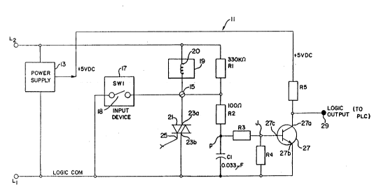
A first embodiment of an I/0 module having a
S combination I/O point, generally designated 11, is
illustrated in Figure 1.
A power supply 13 (with a nominal potential of
24-240 volts AC) is connected between a first line
L1 and a second line L2. The particular voltage
used depends upon the load, though for purposes of
this discussion, 120 volts will be assumed. The
power supply 13 further provides 5 volts regulated
DC, the use of which is discussed below.
A terminal 15 is provided which functions as
the combination I/0 point. If the combination I/0
module 11 is to be used as an input point, an input
device 17, such as a standard mechanical switch 18,
is coupled between the terminal 15 and the first
line Ll. If the combination I/0 module 11 is to be
used as an output point, an output device 19, such
as a coil 20 for a mo~or starter (not shown), is
coupled between the terminal 15 and the line L2.
In certain applications discussed below, the
combination I/0 module 11 is operable simultaneously
as both an input point and an output point. Accord-
ingly, the input device 17 would be coupled between
the terminal 15 and the first line Ll, and the
output device 19 would be coupled between the
terminal 15 and the second line L2.
The combination I/0 point 11 further includes
a triac 21, such as 2N 6073 A, having first and
second power electrodes 23a, 23b, respectively, and
a gate electrode 25. The triac 21 is selectively
switchable between a conductive, or 'on' state and
a non-conductive, or 'off' state, as is well known.
WO91/04538 2 0 6 6 5 7 2 PCT/US90/05119
The combination I/O module 11 further includes
a first resister Rl (330n) coupled between the
second line L2 and the terminal 15, a second resis-
ter R2 (lOOkn) and a snubber capacitor C1 (0.033~F)
S coupled in series between the terminal 15 and the
first line L1. Further included is a transistor 27
having power electrodes comprising a collector 27a
and an emitter 27b, and a control electrode comprise
a base 27c. A third resistor R3 is coupled between
the transistor base 27c and a junction P of the
second resistor R2 with the first capacitor C1. A
fourth resistor R4 is coupled between the first line
L1 and a junction J of the third resistor R3 with
the transistor base 27c. A fifth resistor R5 is
coupled between the 5 volt DC output of the power
supply 13 and the collector 27a of the transistor
27.
Lower values of the first resister Rl will
increase power loss and reduce load detection
sensitivity. Higher values of the first resistor
Rl reduce the base-emitter current IBR f the
transistor 27, increasing noise sensitivity. The
0.033~F value for the snubber capacitor C1 is based
on tests with the power supply 13 at 120 VAC.
Larger capacitance may be necessary for larger
voltages.
The junction of the fifth resistor R5 with the
collector 27a of the transistor 27 provides a logic
output 29 which is utilized by the PLC, as is well
known. As discussed below, the value of the logic
output 29 indicates the status of the input device
17.
Referring to Figure 2, operation of the com-
bination I/0 module 11 as an input point is illus-
trated. The reference numerals relate to thoseelements discussed above with respect to Figure 1.
WO91/04538 ~ 2 0 6 6 5 7 2 pcT/usso/nsl 19
When the input device 17, such as the switch
18, is open, the voltage at the terminal 15 is
determined by the voltage divider R1, R2, C1
(ass~uming the triac 21 is off). A current divider
network comprising the third and fourth resistors
R3 and R4 biases the transistor 27 on during posi-
tive line cycles. With the transistor 27 turned on,
the voltage at the logic output 29 is logic low
during positive half cycles. Thus, an open input
device 17 results in a zero logic state output at
the logic output 29 during positive half cycles.
When the input device 17 is closed, the voltage
at the terminal 15 is shorted to ground, thus
biasing the transistor 27 off for both positive and
negative cycles. With the transistor 27 off, the
voltage at the logic output 29 is held at the 5 volt
DC supply voltage. Thus a closed input device 17
results in a 5 volt, or one logic state output at
the logic output 29 for both positive and negative
cycles.
The combination I/O module 11 utilized as an
output point as illustrated in Figure 3. As with
Figure 2, common reference numerals have been
maintained in Figure 3.
To operate the combination I/O module 11 as an
output point, the output device 19 is coupled
between the terminal 15 and the second line L2.
When the output device 19 is to be activated, the
triac 21 receives a positive, logic on signal from
the PLC (not shown) at the gate electrode 25 of the
triac 21. The logic on signal turns on the triac
21, thus placing the output device l9 between the
first and second lines Ll, L2. Similarly, when the
output device 19 is to be turned off, the triac 21
3S receives a logic off signal from the PLC, turning
off the triac 21 at the next current zero crossing,
WO91/04538 2 ~ 6 6 5 7 2 PCT/US90/05119
and thereby isolating the output device l9 from the
first line Ll. Since the triac 21 acts the same as
the switch 18, the condition of the triac 21 can be
monitored by the transistor circuit to determine if
it is following its logic signals.
The combination I/O module ll is further provi-
ded with load detection circuitry to detect the
presence (or absence) of the output device l9
coupled between the second line L2 and the terminal
15 as well as circuitry to determine whether the
triac 2l indeed turned on in response to a logic on
signal from the PLC.
The following discussion describes how the load
l9 is detected with both the triac 21 and the switch
- 15 17 'off'.
Typically, the impedance of the output device
l9 is significantly lower than the impedance of the
33okn first resistor Rl. Referring still to Figure
3, and assuming for the moment that the output
device l9 is not coupled between the terminal 15 and
the second line L2, the phase of the voltage (Vp) at
the point P relative to the first line L1 will lag
the phase of the voltage (VL2) Of the second line L2
relative to the first line Ll because of the capaci-
tance of the snubber capacitor Cl. Because theimpedance of the output device l9 is less than the
impedance of the first resistor Rl, when the output
device l9 is coupled between the second line L2 and
the terminal 15, the resistance of the first resis-
tor Rl is effectively substantially reduced (infact, Rl typically can be ignored).
In the limit, for example if the resistance of
the output device l9 is on, the voltage Vp would be
in phase with the voltage VL2 . In reality, because
the output device l9 does have some impedance, the
voltages Vp and VL2 will not be completely in phase;
WO91/04538 2 0 6 6 5 7 2 PCT/US90/05119
however, their phases will be much closer than with
no output device l9. Thus, by monitoring the phase
relationship of the voltage Vp relative to the
vol~age VL2 one can constantly monitor the presence,
of absence, of the output device l9.
A circuit for determining the phase difference
between voltages Vp and VL2, and hence the presence
of absence of the output device l9, is illustrated
Figures 4a and b.
A reference circuit 33 provides a square wave
output Vre~ representing the voltage of an I/O point
without a load connected. The reference circuit 33
is the same as the combination I/O module ll, but
it does not have the terminal 15. A first wave form
36 representing the phase of the voltage of the
second line L2 with respect to the voltage of the
-first line Ll is for reference only.
A second wave form 37 representing the phase
of the voltage Vr~f relative to the voltage on the
first line Ll is generated at the collector of the
transistor 27 of the reference circuit 33.
A third wave form 40 representing the phase of
the voltage at the logic output 29 of the combin-
ation I/O module ll with and without a load con-
2S nected demonstrates the effect of the load on thephase of the voltage.
As illustrated, the load wave form is shifted
by an amount t.
One way of detecting this phase delay is by
sampling both the second and the third wave forms
37, 40, respectively, and passing the sampled data
through a respective register of the PLC as a
software oscilloscope of the wave forms 37, 40. By
comparing these two registers, the PLC can determine
the phase difference and, hence, the presence or
absence of the output device l9. The particular
WO91/04538 20 66 5 ~ ~ PCT/~iS90/05119
-- 10 --
sampling rate necessary depends on the impedance of
the components as well as of the output device 19,
as such relative values determine the total phase
dif~erence between load and no-load conditions. In
addition, by memorizing the phase shift for a given
load when the triac 21 is off, one can detect
changes in load characteristics such as the begin-
ning failure of a motor starter coil.
The above discussion permits the com~ination
I/O module 11 to detect the presence or absence of
a load when the triac 21 is off. Detection of the
presence or absence of a load when the triac 21 is
on is illustrated in Figure S.
Figure S illustrates the relationship between
the load current through the triac 21, IL1 versus
- the gate voltage Vc for the triac 21. An "ideal"
curve is illustrated in phantom while an actual
curve is illustrated in solid
According to the ideal curve, there is a first
20 gate voltage VG1 for all load currents greater than
the gate current IG and a second gate voltage VG2
for all load currents less than the gate current I~.
As illustrated however in the actual curve, there
is a rounding of the curve about the gate current
25 value in a progressive decline in the gate voltage
with increased negative load current. The actual
curve for a given triac is independent of the actual
impedance of the load. In order to detect whether
the triac 21 is actually conducting load current,
one can detect the shift in the level of VG ~etween
positive and negative current. In the event that
the gate voltage VG does not change, one knows that
the triac 21 is not conducting.
Referring again to Figure 1, one application
of the combination I/O module 11 illustrates how it
can ~e used to permit a mechanical input, such as
2066S72
WO91/04538 ~ ~ PCT/US90/05119
-- 11 --
the switch 18, to operate both a direct output as
well as a software input. The input device 17 is
coupled between the first line L1 and the terminal
15 and the output device 19 on which one desires to
perform the direct output, for example to turn on
an indicator light, is coupled between the terminal
15 and the second line L2 when the switch 1~ is
closed, the indicator light is coupled directly
between Ll and L2, bypassing the triac 21. In
addition the logic output 29 goes from logic state
zero to one on positive half cycles. Thus one can
have a positive indication of the status of the
switch 18 as well as a software indication thereof.
The combination I/O module 11 can also be used
to replace a motor starter circuit which previously
would have required three inputs and one output, as
illustrated in Figures 6a, b and c. A traditional
motor starter circuit is illustrated Fiqure 6~. The
circuit includes a starter switch 51, a stop switch
53, various limit and emergency stop switches
generally designated 55, a starter coil Cs and a
starter relay Rs~ As is well known, when the
starter switch 51 is closed, assuming the switches
53 and 55 are also closed, current from lines L1 to
L2 energizes the starter coil Csl closing the
starter relay Rs~ bypassing the starter switch 51.
As long as the stop switch 53 and the emergency/
limit switches 55 remain closed, the starter coil
Cs will remain energized and the starter relay Rs
will stay closed, thereby providing continuous power
to the motor. Typically to automate this function,
a minimum of 4 points; three inputs and one output
would be required. The three inputs would be from
the starter switch 51, the stop switch 53 and the
emergency/limit switches 55; and the output would
~e to the motor (not shown~.
2066572
WO91/04538 PCT/US90/05119
- 12 -
As illustrated in Figure 6b, a motor starter
circuit utilizing the combination I/O module 11 of
the present invention can be performed using a
sin~le point. Accordingly, the starter switch 51
is wired between the first line Ll and the terminal
15; the stop switch 53, the emergency/limit switches
55 and the motor are wired in series between the
terminal 15 and the second line L2. The triac 21
is illustrated in phantom as extending between Ll
and 15 (See Figures 1-3).
Software which would be resident in the PLC,
to perform the above is illustrated in Figure 6c in
ladder diagram form. A rung 61 includes a first
relay 63 which is normally open, until continuity
between Ll and the terminal 15 is established. The
rung 61 further includes a second relay 65 which is
open until continuity between the terminal 15 and
the second line L2 is detected. A coil 66
represents the status of conduction of the triac 21.
Parallel to the first relay 63 is a third relay 67
which is closed upon energization of the coil 66.
Accordingly, when the starter switch 51 closes,
the module 11 detects continuity between the first
line Ll and the terminal 15. One then measures
continuity between the terminal 15 and the second
line L2 as discussed above with respect to determi-
ning the presence of a load. If continuity is
detected between the terminal 15 and the second line
L2, this energizes the continuity coil 66, thereby
closing the relay 67. The relay 67 will remain
closed until continuity between terminal 15 and the
second line L2 terminates, such as actuation of the
stop switch 53 or the emergency/limit switch 55.
Typically, an input or output module contains
more than one point. Accordingly, in the preferred
embodiment, the module 11 actually contains 16
WO91/04538 2 Q 6 6 5 7 2 PCT/US90/0~119
points, each of which is operable as an input point,
an output point, or both, as illustrated in Figure
7. The logic outputs 29 of the first eight I/O
poi~ts are coupled via a first multiplexor 71 (LS-
244) to a data bus 73. Similarly, the 9th through
16th I/O points are coupled via a second multiplexor
77 (LS-244) to the data bus 73. The output of the
reference circuit 33 is connected to an interrupt
pin of a PLC, allowing phase detection of the other
I/O points.
An alternate embodiment of the invention is
illustrated in Figure 8. Common reference numerals
have been maintained. As with the first embodiment,
the input device 17 is coupled between the terminal
15 and the first line Ll, and the output device 19
is coupled between the terminal 15 and the second
line L2. The logic in signal from the PLC turns on
the triac 21 providing power to the output device
19. Further, when the input device 17 is open, the
voltage at the logic output 29 is zero, and when the
input device 17 is closed the voltage at the logic
output 29 is 5.1 volts, a logical 1. As also with
the first embodiment, in the second embodiment, the
presence or absence of the load 19 when the triac
21 is off is detected by monitoring the phase dif-
ference between the phase of the voltage of the
second line L2 relative to the first line Ll with
the phase of the voltage at point P relative to the
first line Ll. Further, detection of operation of
triac current is performed by monitoring changes in
the gate voltage VG-
Although explained with respect to an I/O
module, it should be understood that the technique
for detecting whether a triac is conducting current
by monitoring its gate voltage is equally applicable
W O 91/04538 2 ~ 6 6 5 7 2 PC~r/US90/05119
- 14 -
to any device utilizing a triac, and this aspect of
the invention should be accordingly interpreted.
It will be understood that the invention may
be e~bodied in other specific forms without depar-
ting from the spirit or central characteristicsthereof. The present examples and embodiments,
therefore, are to be considered in all respects as
illustrative and not restrictive, and the invention
is not to be limited to the details given herein.