Note: Descriptions are shown in the official language in which they were submitted.
W~ 91/07721 ,,~ ~PCT/US90/06322
--1--
2066626
ERROR CORRECTION METHOD AND APPARATUS
BACKGROUND
l. Field of Invention
This invention pertains to method and apparatus
for error correction of stored or transmitted data, and
particularly for correcting errors occasioned by the loss
5 of entire blocks or a plurality of blocks of information
recorded on storage medium.
2. Prior Art and Other Considerations
For decades digital information has been
recorded on magnetic media, including magnetic tape and
magnetic disks. Unfortunately, noise occurring in the
storing of data on the media, or in the reading of data
from the media, can result in errors. To alleviate this
problem, various encoding techniques have been developed
to specially encode the transmitted or stored data in
order to afford error correction capability.
Typically the digital information is stored in
the form of physical blocks of data, with each block
consisting of a plurality of bits. In accordance with
prior art error encoding techniques, within each block
sets of information or message bits have check bits
appended thereto to form a codeword. The check bits for
the codeword are derived by an encoder which operates on
the set of information bits using a predetermined code,
such as a Reed-Solomon code. The encoder imparts desired
properties to the codewords so that, upon subsequent
reading of the blocks, the codewords can be decoded in
such a manner that errors are discernable and
correctable. An example of a decoder is provided in
United States Patent 4,845,713 to Christoper P. Zook,
entitled METHOD AND APPARATUS FOR DETERMINING THE
. ' ' ' . '` ::,; ,. ~' ' ' ''~
.. .. ... . . . . .
... .
WO91/07721 6 ~ 2- PCT/US901~6322
COEFFICIÉNTS OF A LOCATOR POLYNOMIAL, which is
incorporated herein by reference.
Operating upon a block, two or more codes can
be combined to produce a more powerful code and to offer
an essentially second level of error correction for the
block. Such a combintation of codes is known in the
literature as "two dimensional codes" or "product codesi'O
An example of an error correction system operating with
product codes is provided in United States Patent
4,845,714 of Christopher P. Zook, entitled MULTIPLE PASS
ERROR CORRECTION PROCESS AND APPARATUS FOR PRODUCT CODES,
which is incorporated herein by reference.
Current error correction schemes are generally
sufficient for correcting errors that occur within a
block of recorded information. Yet there are occasions
when entire blocks are unreadable. Even worse, at times
a plurality of blocks may be unreadable. Error
correction at the block level, with error correction bits
embedded in the block, is of no avail when one or more
entire blocks are lost.
One example of the problem of block loss occurs
in the environment of helical scan recording. In a
helical scan arrangement, travelling magnetic tape is
partially wrapped around a rotating drum so that heads
positioned on the drum are contiguous to the drum as the
drum is rotated. A write head on the drum physically
records data on the tape in a series of discrete stripes
oriented at an angle with respect to the direction of
tape travel. The data is generally formatted into a
plurality of physcial blocks per stripe. Examples of
helical scan recording systems are provided in US Patent
4,843,495, US Patent 4,835,638, and US Patent 4,845,577.
In helical scan technology, there are two
motions with respect to the tape. A first motion is the
movement of the heads which follow a diagonal stripe
across the tape to write and/or read blocks in the
stripe. A second motion is the linear motion of the tape
'' . ,' :. - -: :
~. ' , ' ~ .
.
,~
~ f ~
WO91/07721 PCT/US~ 6~
_3_ ~ ?2 0i~6 2 6
from reel-to-reel and over tape guides.
Accordingly, in helical scan technology there
are also two types of error that can occur as a result of
these two motions. The first type of error destroys
multiple blocks in a stripe. A second type of error
destroys blocks in the same position in consecutive
stripes (i.e., blocks aligned in the direction of tape
travel). Current error correction coding techniques do
not address the destruction of a plurality of blocks.
- Accordingly, it is an object of the present
invention to provide method and apparatus for correcting
errors involved in the recordation or reading of
information on storage media.
An advantage of the present invention is the
provision of method and apparatus which facilitates the
correction of errors involving the loss of an entire
block of data stored on or read from storage media.
A further advantage of the present invention is
the provision of method and apparatus which facilitates
the recreation of an entire stripe or row of blocks of
data lost during storing or reading from storage mediaO
SUMN~RY
- In a method of encoding and decoding
informational data for transmission to a storage medium,
a group G of physical blocks written to the storage
medium includes both user data information blocks and
auxiliary error correction blocks. Each block (BrC)
included in the group G belongs both to a row r and a
column c. Informational data is formatted into
preselected bit positions of the user data information
blocks. Values for bit positions in the auxiliary error
correction blocks are generated by performing an
exclusive OR operation upon values in corresponding bit
positions in a subgroup of strategically selected user
data blocks. By strategically selecting the user data ;
blocks to be included in the subgroup, the method
facilitates recovery of entire blocks, and even rows or
,
: -
WO91/07721 PCT/US9~6~2
6;~ 6 2 ~ 4
columns of blocks.
In a preferred mode of the invention, the
columns of each group G are each written as helical
stripe on magnetic tape by a helical scan recording
system, with the informational data blocks recorded in
stripes that precede stripes containing the auilliary
error correction blocks. Each stripe comprises k number
of blocks; each group G comprises n number of stripes.
Also according to a preferred mode of the
invention, m number of error correction blocks E; are
generated for inclusion in the group of blocks BrC. In
this regard, i ranges from 0 to m-l, and m = q x k with q
being an integer constant. The value of each bit
position included in each auxilary error correction block
E; is derived from the sum of the bits having the
corresponding bit position in all blocks BrC where i =
(r + k(c mod q) + INT(c/q)) mod m. Each auxilary error
correction block has stored therein a bit indicating that
the block is an auxiliary error correction block. Blocks
recorded in a stripe following a stripe of auxiliary
correction blocks have stored therein a bit indicating
that the block is not an auxiliary correction block.
- Using conventional error correction techni~ues,
error correction bits are inserted both into the user
data blocks and into the auxilary error correction blocks
in other bit positions.
BRIEF DESCRIPTION OF THE DRAWINGS
The foregoing and other objects, features, and
advantages of the invention will be apparent from the
following more particular description of preferred
embodiments as illustrated in the accompanying drawings
in which reference characters refer to the same parts
throughout the various views. The drawings are not
necessarily to scale, emphasis instead being placed upon
illustrating the principles of the invention.
Fig. l is a schematic view of head placement on
a drum of a helical scan system of an embodiment of the
: ' ~ ' :~: .:
~ 91/07721 PCTtUS90/~63~
_5_ l' .~ 2~a`6~6~26
invention.
Fig. 2 is a schematic view of the helical scan
system of the embodiment of Fig. 1 recording stripes on
magnetic tape.
Fig. 3 is a schematic view an AUXECC generator
included in the helical scan system of the embodiment of
Fig. 1.
Fig. 4 is a schematic view of the helical scan
system facilitating the head placement on a drum
according to the embodiment of Fig. 1.
Fig. 5 is a schematic view depicting the format
of a magnetic tape recorded by or readable by the helical
scan system of the embodiment of Fig. 1.
Fig. 6 is a schematic view of a plurality of
stripes recorded on magnetic tape by the helical scan
system of the embodiment of Fig. 1, and further showing
paths of travel of heads provided on the drum of the ! ,
helical scan system of the embodiment of Fig. 1.
Figs. 7A - 7C are schematic views depicting the
format of Track 1 and Track 2 of a magnetic tape recorded
by or readable by the helical scan system of the
embodiment of Fig. 1.
- Fig. 8 is a schematic view depicting the format
of a physical data block included on a stripe of magnetic
tape recorded by or readable by the helical scan system
of the embodiment of Fig. 1.
Fig. 9 is a schematic view depicting the format
of a physical block header of a physical data block
included on a stripe of magnetic tape recorded by or
readable by the helical scan system of the embodiment of
Fig. 1.
Fig. 10 is a schematic view depicting a group
of stripes, including an AUXECC stripe, recorded on
magnetic tape by by the helical scan system ~f the
embodiment of Fig. 1.
Fig. 11 is a schematic view depicting a
plurality of groups of stripes, including an AUXECC
: , .: -
:, ' , -. ~ ~. , -
: : ~ '
WO91/07721 PCT/US9~06~ ~
Q`~662~ -6-
stripe, recorded on magnetic tape by by the helical scan
system of the embodiment of Fig. l.
Fig. 12 is a schematic view depicting an
alternate manner of generating AUXECC blocks.
DE~AILED DE8CRIPTION OF THE DRAWINGS
Fig. l shows drum and transport portions of a
helical scan system 30 for recording digital information
on magnetic tape 32. The helical scan system 30 includes
a tape transport 34 and a rotating drum 36.
The tape transport 34 includes a capstan 42 and
two tape guides 44. In conventional manner, the capstan
42 is rotated by an unillustrated capstan drive motor in
order to move the tape 32 in a direction of tape travel
indicated by arrows 46. In the illustrated embodiment,
the capstan 42 rotates to transport the tape 32 at a
speed on the order of about one-half inch per second.
DRUM AND HEAD STRUCTURE
The drum 36 is rotatable about drum axis 50~
The drum is rotated at a velocity of about 1800 rpm by an
unillustrated drum motor. An unillustrated tachometer
detects rotations of the drum motor shaft, and hence of
the drum, and produces a DRUM SYNC signal. As shown in
Fig. 2, drum axis 50, and hence drum 36, is angularly
oriented with respect to the edges and direction of
travel of the tape 32. The drum 36 has a drum upper
surface 52 and a drum lower surface 54, both of which are
planar. The drum axis 50 is orthogonal to both the drum
upper surface 52 and the drum lower surface 54. The drum
36 also has a peripheral surface 56 which wraps around
the circumference of the drum 36.
The peripheral surface 56 of the drum 36 has
two sets of heads mounted thereon, in particular a first
set of heads comprising write heads Wl and W2 and a
second set of heads comprising read heads Rl and R2. In
addition, the peripheral surface 56 of the drum 36 has a
servo h~ad S mounted thereon.
. . - :
. - .
: ' ,. ''''''
91/07721 PCT/US~ 6~2
~7~ 'i~2~ 6~a2 6
The heads Wl, W2, Rl, and R2 are mounted to
generate helical stripes on the magnetic tape 32 in the
manner shown in Fig. 6. Heads Wl and W2 essentially
simultaneously write first and second tracks of data,
i.e., tracks Tl and T2, respectively, on the tape 320
Heads Rl and R2 are positioned to read tracks Tl and T2~
respectively, 180 degrees after the tracks Tl and T2 are
written. In this respect, although Fig. 6 shows write
heads Wl, W2 and read heads Rlj R2 traveling over trac~s
Tl and T2 for the sake of depicting head placement
relative to the tracks, it should be understood the read
heads Rl, R2 and the write heads Wl, W2 cannot
simultaneously be over the tracks in the manner depicted
in Fig. 6. Likewise, the inclusion of the servo head S
in Fig. 6 is merely to show the position of the servo
head S relative to the tracks Tl and T2, and not in
relationship to the read heads Rl, R2 or the write heads
Rl, R2.
In the above regard, four geometrical factors
regarding the heads are strategic to enable the
simultaneous writing by heads Wl and W2 and the
subsequent respective reading by corresponding heads Rl
and R2; the angular separation of the heads about the
drum peripheral surface 56; the axial location of the
heads relative to one another; the width of the heads;
and, the azimuthal orientation of the heads. These
geometrical factors are explained further in United
States Patent Application Serial Number 07/433,961,
entitled DUAL CHANNEL HELICAL SCAN RECORDER, which is
incorporated herein by reference.
Fig. 6 shows a plurality of helical stripes
recorded on magnetic tape 32 by the helical scan system
30, and the ultimate paths of travel of the heads Wl, W2,
Rl, and R2, as well as the servo head S over the helical
stripes. The direction of movement of the heads is
depicted by arrow 78 in Fig. 6.
.
. ~ .
W091/07721 PCT/US~fO632~ ~
20$6~26 -8-
Thus it is seen that a dual channel helical
scan system 20 is provided, with a first channel
including the heaAs Wl and Rl, and a second channel !
including the heads W2 and R2. The employment of two
channels effectively doubles the data transfer rate
since twice as many tracks are written to tape per
revolution of the drum 36. For-checking purposes, the
heads Rl and R2 read back the two simultaneously written
tracks approximately 180 degrees after the tracks are
written. The write and read functions occur exclusivel~,
thereby eliminating any crosstalk problems.
SYSTEM STRUCTURE
Fig. 4 illustrates the overall helical scan
system 30, including the read heads Rl, R2, the write
heads Wl,W2, and the servo head S. The helical scan
system 30 further includes a control microprocessor 100
which communicates primarily with a mailbox 102; a SCSI
interface 104; a data buffer manager 106; an
encoder/formatter 108; a decoder/de-formatter 110; and,
an AUXECC block generator 111.
The data buffer 106 manager comprises a data
buffer which includes 1 MByte of DRAM is organized as a
9-bit wide, dual-port, circular memory. Data transfers
between the data buffer manager 106 and the SCSI
interface 104, the encoder/formatter 108, the decoder/de-
formatter 110, and the AUXECC block generator 111 occur
asynchronously or synchronously. Logical user data
blocks are formatted into physical blocks in the data
buffer 106 for recording onto tape.
The AUXECC block generator 111 produces
auxiliary error correction blocks for recording error
correction stripes on the tape 32. The structure and
operation of the AUXECC block generator is further
described herein.
The encoder/formatter 108 receives data blocks
from the data buffer manager 106 and from the AUXECC
block generator 111. The encoder/formatter 108 performs
: : . , .,:,: ,
. , . .. ... , , .~, , ::.
~ ' - : ~ , . :
WO91/07721 PCTIUS90/~63~2
--9-- ~ ~ ~ 6 g Z 6
a variety of functions, including appending error
correction code (ECC) information, inserting
synchronization markers, inserting search fields, and
inserting servo fields and perform interleave sequencing
of bytes. The encoder/formatter 108 transmits the data
blocks and appended information to a RLL Modulator 112
which performs the run-length encoding of the data stream
by translating each 8 bit byte to a 10-bit word. The 10-
bit word is ten transmitted to a bit serializer 114. The
lo bit serializer 114 is connected to a write driver circuit
116 (for write head Wl) through a FIF0 register 118, and
to a write driver circuit 120 (for write head W2). The
function of the FIFO register 118 will be explained below
in connection with the description of the write operation
of the helical scan system 30.
The read heads R2 and Rl are connected to
preamplifiers 130 and 132, respectively, for amplifying a
read signal. The preamplifiers 130 and 132 are connected
to signal conditioning circuits 134 and 136,
respectively. The signal conditioning circuits 134 and
136 include circuits for amplitude sensing, equalization,
and data clocking and detection.
The signal conditioning circuit 134 is
connected to FIF0 register 138, which in turn is
connected to a serial-to-parallel converter 140. The
signal conditioning circuit 136 is connected directly to r
the serial-to-parallel converter 140.
The serial-to-parallel converter 140 is
connected to an RLL De-Modulator 142 and to a pattern
detector circuit 143. The RLL Read Modulator basically
performs the inverse operations of the corresponding RLL
Write Modulator 112.
The pattern detector 143 monitors the incoming
stream of data in order to recognize a synchronization
field. When the pattern detector 143 has recognized a
predetermined number of synchronization fields having a
predetermined spacing, the pattern detector 143 generates
.
.
WO91/07721 PCT/US9~/~632~
-i2Q~G2~ 6 -lo-
a BKRDY signal. In addition, the pattern detector 143
supplies to the serial-parallel converter 140
synchronizing signals necessary for the operation of the
converter 140.
The RLL De-Modulator 142 is connected to the
decoder/de-formatter 110. The decoder/de-formatter 1~0
assembles data blocks and performs error correction.
The microprocessor 100 communicates through its
mailbox 102 with a servo microprocessor 150 and a motion
control system 152. The motion control system 152
includes a dedicated microprocessor for communicating
with a drum servo 156; a capstan servo 158; reel control
circuits 160; and a mechanical controller 162. In
addition, upon receipt of the BKRDY signal generated by
the pattern detector 143, the motion control system 152
includes circuitry, herein called HEAD SYNC generator
164, for developing a HEAD SYNC signal. The HEAD SYNC
generator 164 is described in United States Patent
Application Serial Number 07/434,008 entitled METHOD AND
APPARATUS FOR SYNCHRONIZING TIMING SIGNALS, which is
incorporated herein by reference. The HEAD SYNC signal
is high when the read heads Rl and R2 are over the
helical stripes of Track 1 and Track 2. The HEAD S~NC
signal is low when the write heads W1 and W2 are over the
stripes of Track 1 and Track 2.
Thè motion control system 152 also communicates
with sensor interface circuits for the various
unillustrated elements including the following: a drum
tachometer; a capstan tachometer; a reel tachometer; an
end of tape (EOT) detector; and, a beginning of tape
(BOT) detector. As shown in Fig. 4, the tape transport
system 34 is connected to the drum servo 156, the capstan
servo 158, the reel control 160, and the mechanical
controller 162.
The servo head S has its output signal
connected to preamplifier 172. The output of the servo
preamplifier 172 is applied to a filter and detection
- ~ . . .. .
. ' . ~ : ' '
W091/07721 PCT/US90/~32~
~ ~.
g ~ ~
circuit 174 which filters the amplified signal and for
detecting the servo signals recorded on tape. The filter
and detection circuit 174 is in turn connected to a servo
tracking circuit 175 included in the motion control
system 152. The details of servo tracking circuit 175
are shown in United States Patent Application Serial
Number 07/433,977 entitled SERVO TRACKING FOR HELICAL
SCAN RECORDER, which is incorporated herein by reference.
TAPE FORMAT
Fig. 5 depicts the format of magnetic tape 32
for the helical scan system 30. The tape 32 has a
physical beginning of tape (PBOT) 300 located at the
point where a translucent leader material is attached to
the magnetic media. Downstream from the PBOT 300 (in the
sense of direction of tape transport as shown by arrow
78) are a multitude of helical stripes formed on the
magnetic tape media. The helical stripes contain, of
course, the information written by the write heads Wl and
W2 and read by the read heads Rl and R2. The format of
the helical stripes is discussed subsequently in
connection with Figs. 6 and 7. At the end of the tape 32
is a physical end of tape (PEOT) 302.
Since the helical scan system 30 is a dual
azimuthal system, in a write mode odd numbered helical
stripes are written at a first azimuthal angle A1 by
write head W1 and even numbered helical stripes are
written at a second azimuthal angle A2. In a read or
readback mode, odd numbered helical stripes are read at a
first azimuthal angle Al by write head Wl and even
numbered helical stripes are read at a second azimuthal
angle A2. As can be discerned from the foregoing, the
first azimuthal angle Al is +20 degrees; the second
azimuthal angle A2 is -10 degrees. As used hereinafter,
any helical stripe written by write head Wl or read by
read head R1 is referred to as "Track l". Likewise, any
helical stripe written by write head W2 or read by read
head R2 is referred to as "Track 2".
- ~ .
WO91/07721 PCT/US~ 2~
2 ~ r. ~t
For the purposes of the present invention, it
is sufficient to know that both Track 1 and Track 2
include a plurality of data blocks 317, also known as
physical data blocks. In the illustrated embodiment,
both Track 1 and Track 2 contain eight (8) such data
blocks 317. Other aspects of the format of Track 1 and
Track 2 are understood by reference to United States
Patent Application Serial Number 07/433,961 entitled DUAL
CHANNEL HELICAL SCAN RECORDER, which is incorporated
herein by reference.
Fig. 8 shows the format of each the data blocks
317 provided in both Track 1 and Track 2~ The format for
the data blocks 317 is the same, regardless of whether
the data block 317 is written on Track 1 or Track 2. As
shown in Fig. 8, each data block 317 (also known as a
"physical data block") includes a physical block header
350 (of 14 bytes); a data area 352 (of 1024 bytes); an
error correction code ("ECC") area 354 (of 400 bytes),
and, a cyclical redundancy check ("CRC") area 356 (of 2
bytes).
Fig. 9 depicts the format of the physical block
header 350 of.each physical data block 317. Fig. 9 shows
a hexidecimal numbering scheme for the physical block
header 350. The header 350 is used to determine the type
of information contained in the block 317, e.g., the
block type, and how the information is stored. As
indicated above, the header 350 consists of 14 bytesO
The four lower order bits of byte 0 of the header 350
contain a value (identifier BLOCK TYPE) which indicates
the typing of the block 317. The following hexadecimal
values are associated with different block types: "OH"
represents user data; "AH" represents a filemark; "CH"
represents a logical beginning of tape (LBOT) write with
retry; "DH" represents a LBOT write with no retry; "EH"
represents a gap; and, "FH" represents end of data.
As indicated above, a BLOCK TYPE value of "OH"
signifies that a physical block 317 contains user data.
- : .... . , . ~
WO 91/07721 PCI/US9~/~63~2
-13- ~ ~2~6~6 6 2 6
Such a block 317 is referred to as a User Data Block. A
User Data Block is a physical block which can contain up
to 1024 bytes of user data in the data area 352.
Of interest to the present invention is the
fact that the physical block header 350 includes an
AUXECC field and an INIECC field. In this regard, the
AUXECC field (byte 0, bit 7) indicates that the
information contained in the data area of 8 consecutive
blocks contains auxilliary ECC data for the preceding 128
block of data. The INIECC field (byte 0, bit 6)
indicates that the 8 consecutive blocks are the first 8
block of a set of 128 blocks for which 8 auxillary ECC
data has been written to the tape. The WRTRTY field
(byte 0, bit 5) indicates if this block has been
previously written.
STRUCTURE: AUXECC CIRCUIT
The AUXECC circuit lll includes an AUXECC RAM
702 which is used to store data for generating an AUXECC
stripe on the magnetic tape 32. Fig. lO shows a segment
of tape 32, and a group G of sixteen helical stripes 704
- recorded thereon, particularly stripes 7040 - 70415.
Concerning the constituency of stripe group G,
stripes 7040 ~ 7414 inclusive are stripes wherein the
physical data blocks 317 (described above) contain user
informational data and error correction information.
Stripe 70415 is an AUXECC stripe, generated in the manner
described below, which offers an additional layer or
dimension of error correction capability. In this
regard, the AUXECC stripe 7415 is used for error
correction purposes when a conventional error correction
circuit provided in the decoder/de-formatter llO is
unable to decode one or more blocks.
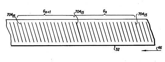
Fig. ll shows a segment of tape 32 including a
plurality of stripe groups G, namely group Gn and group
Gn,1. The last stripe, i.e. stripe 70415 of each group G
is an AUXECC stripe and is shown somewhat darker than the
other stripes in the group for illustration purposes.
..
.
-
.
WO91/07721 PCT/US9~/~632 ;
~`~;;'2 0,~ 2 6 -14-
Thus, it is seen that a multitude of successive groups G
are provided on the tape 32.
Returning now to the structure of the AUXECC .
circuit 111 as described in Fig. 3, the AUXECC RAM 702 is
sized to accommodate eight blocks. In addition to the
AUXECC RAM 702, the AUXECC circuit 111 includes an
address generator 710; a controller 712; an address
multiplexer (MUX) 714; an XOR circuit represented by XOR
gate 716; and, a data transmission MUX 718.
A stream of eight bit data enters the AUXECC
circuit 111 on a line designated DATA-IN in Fig. 3. As
described below in connection with the operation of the
AUXECC circuit 111, in a write mode the data on line
DATA-IN is received from the buffer manager 106 (see Fig~
4). In a read mode the data on line DATA-IN is the
stream of.data received from the RLL De-Modulator 142~
The eight bit data on line DATA-IN is connected
both to input terminal 0 of MUX 718 and to the XOR
circuits 716. Although not expressly shown as such, it
should be understood that the XOR gate 716 represents
eight such XOR gates, one gate for each bit of
information carried on line DATA-IN. Likewise, MUX 718
represents~a bank of eight multiplexers, one for each bit
of information carried on line DATA-IN.
Output terminals of the XOR circuit 716 are
connected to the eight data input pins of the AUXECC RAM
702. The eight output pins of the AUXECC RAM 702 are
connected to input terminal 1 of the MUX 718. In
addition, the eight output pins of the AUXECC RAM 702 are
connected to input terminals of eight respective AND
gates represented by AND gate 726, the output terminals
of which are connected to respective XOR gates in the XOR
circuit 716.
The address generator 710 generates an address
for application via the address MUX 714 to the AUXECC RAM
702. The address generator 710 includes a byte-counter
730; an OR gate 731; a block counter 732; a stripe
.: ~ , . . :, , -
:,:, . . .
: . ::: ' :
W 91/07721 PCT/US90106322
-15- ~ 2 ~ ~6~2 6
counter 734; and, an adder 736.
The AUXECC circuit 111 is informed via line
BYTE CLOCK when a new byte is being applied on line DATA-
IN. In this respect, circuitry is elsewhere provided for
pulsing a line BYTE CLOCK for each transmission of bits
passed over the line DATA-IN.
The BYTE CLOCK signal is applied to a count
enable pin of the byte counter 730. The data output pins
of the byte counter 730 are connected to terminal O of
the address MUX 714. As is understood, the address MUX
714 actually represents a plurality of multiplexers
corresponding to the number of bits in the address.
A carry output of the byte counter 730 is
connected through OR gate 731 to the count enable pin of r
the block counter 732. The block counter 732 has its
three data output pins connected to a first port of the
adder 736.
A carry output pin of the block counter 732 is
connected to an enable count pin of the stripe counter
734. The stripe counter 734 has its three lower order
data output pins connected to both a second port of the
adder 736 and to the logic controller 712.
The three lower order output pins of the adder
are connected by a line 437 to the three higher order
input pins of terminal O of the address MUX 714.
Fig. 3 also shows an intra-block error
correction circuit 740, which is more properly included
in the decoder/de-formatter~llO but illustrated in Fig. 3
for convenience. The error correction circuit (ECC) 740
is connected to apply a signal to the select pin of MUX
714 and to the logic controller 712. The ECC circuit 740
is also connected to apply a BLOCK COUNT INCREMENT pulse
on line 741 to OR gate 731 whenever the ECC circuit 740
is unable to decode a block of data. The ECC circuit 740
is also connected to the MUX 714 to apply the address of
an error block to terminal 1 of the MUX 714. Moreover,
the ECC circuit 740 is connected to receive a BAD BLOCK
WO 91/07721 PCI/US9~0632h
` `2U~i66~6 -16-
ADDRESS value on line 743.
The select pin of the data transmission MUX 718
is connected by line 742 to an output of the logic
controller 712. The logic controller 712 informs the ~UX
718 to accept data at one of the terminals 0 or 1
thereof. The logic controller 712 also has an outpu1~
terminal connected by line 724 to a second terminal of
the AND gate circuit 726.
OPERATION: AUXECC ENCODING
As mentioned previously, in helical scan
technology there are two types of error that can result
from two types of motions. The first type of error
destroys multiple blocks in a stripe. A second type OI
error destroys blocks in the same position in consecutive
stripes (i.e., blocks aligned in the direction of tape
travel).
In order to overcome the problem of lost
blocks, and of lost stripes and rows of blocks, as
described above with reference to Figs. 10 and 11, the
AUXECC block generator 111 of the present invention
generates a stripe 70415 of AUXECC blocks for every group
G stripes. The AUXECC stripe 70415 is physically the last
stripe in a group. -
AUXECC blocks E; included in the AUXECC stripe
70415 are obtained by performing an exclusive or ("XOR")
operation with other blocks in a sub-group i of the group
G. Each AUXECC block E; is a member of a sub-group i,
with the other members of the subgroup i being specially
chosen, in the manner described below, to permit recovery
of entire stripes and rows.
By stating that an exclusive or (XOR) operation
is performed with other blocks of a sub-group, what is
meant is that each bit of a block in the subgroup is
XORed with a corresponding bit in other blocks in the
sub-group.
Fig. 10 shows each stripe 704 divided into
eight blocks. Each block is generically represented as
, . . -
,. . ... .
~ 91/07721 - PCT/US90/0632~
~ -17~ 2~ 6 6 6 2 6
BrC. Each block belongs to a row "r" (running parallel
to the direction of tape travel as indicated by arrow 46)
and a column, or stripe, "c". For example, block B20 as
illustrated in Fig. lO is the block in row 2, stripe 0,
actually shown as block C20 having the same subscripts
r,c as the generic block designator B20.
A sub-group formulation and arrangement for the
helical scan system 30 of the illustrated embodiment is
shown in Fig. lO. In lieu of the generic block
designation, each block is shown as having one of the
alphabetical letters A, P, C, D, U, F, G, or H indicative
of the sub-group to which it belongs (letters P and U
being used to avoid confusion with generic identifiers)O
The alphabetical sub-group letters are subcripted to
indicate the row and stripe number where the block is
physically located in the group G.
According to the organization of Fig. lO, the
sub-group i = A is composed of the blocks Aoo; A7~;
A ; As 3; A44; A3s; A26; A17; Ao~B;A7~9; 6,10 5,11
A412; A313; A2,14; and, A11s. As another example, sub-
group i = U is composed of the blocks U4 o; U3 1; U2 2;
U1,3; U0,4; U7,5; U6,6; U5,7; U4,8; U3,9; U2,10; U1,11; U0,12;
U7 13; U6 14; and~ Us1s
Thus, the sub-group formulation and arrangement
for the helical scan system 30 of the illustrated
embodiment is obtained by a shifting selection o~ blocks
BrC. The shifting selection is particularly implemented
by the address generator 710 included in the AUXECC
circuit lll, as will be described further below. The
shifting selection of blocks for inclusion in a sub-group
enables recovery of entire rows and columns.
A generic description of the sub-group
formulation relationship is now provided. Assume that
each group G consists of "n" number of stripes or columns
and "k" number of rows. Assume further that "m" number
of AUXECC blocks E are to be generated for the group G,
where m = q x k (i.e, q multiplied by k) with q being an
..; ~
,
WO91/07721 PCT/US901~ t~
'~
! ~ 2 O 6 ~ --l8--
integer. Each of the bits bx in error block E;
corresponding to user data in the user data blocks is
logically XORed with corresponding bits of the user data
blocks also included in the sub-group i. For the
formulation relationship described above, the values of
each bit position bx included in each block Ej is derived
from the logically XORing of the bits having bit position
bx in all blocks BrC where
l0 [Eqn. l] i = ( r + k(c mod q) + INT(c/q)) mod m
in which INT(c/q) is the largest integer not greater than
c/q). Thus, solving the foregoing equation Eqn. l for i
for any given block BrC yields the sub-group
15 classification i for that block.
The foregoing generic equation Eqn. l is
implemented by the AUXECC circuit lll of the illustrated
embodiment using k (the number of rows per stripe) = 8, n
(the number of stripes per group g) = 16; and m (the
20 number of AUXECC blocks) = 8. The address generator 710
particularly implements the foregoing equation Eqn. l and
the block shifting scheme illustrated in Fig. l0.
During a record operation, data to be encoded
and recorded on tape is supplied to the AUXECC circuit
25 lll on line DATA-IN from the data buffer manager 106. As
each byte is applied on the line DATA-IN, the BYTE CLOCK
signal is pulsed, so that the byte counter 730 counts the
number of bytes. The byte counter 730 counts up to the
maximum number of bytes in a block (1048). The count of
30 counter 730 is applied as the lower l0 bits of an address
to terminal 0 of the address MUX 714.
When the byte counter 730 exceeds it maximun
count capacity, as will occur when all the bytes of a
block are counted, the carry signal of the byte counter
35 730 is used to increment the block counter 732. The
count of the block counter 732 is applied to the adder
736. When the block counter 732 reaches its maximum
' ' , . ~
-: - - ~: .: '
, , ~ ,. ~
WO91tO7721 PCT/US90/06~2
~ . ~.
~i` 206662~
count of eight (the number of blocks in a strlpé), the
block counter carry signal is applied to the stripe
counter 734. .
Using the carry signal from the block counter
732, the stripe counter 734 counts the number of stripes
of data passing through the AUXECC circuit 111 for the
group G. The contents of the stripe counter 734 is
applied both to the adder 736 and to the logic controller
712.
The adder 736 functions to add the two numbers
represented by the values in the block counter 732 and
the stripe counter 734, and to perform a "modulo 8"
operation with respect to those two values. By taking
the lower three bits of the sum, the modulo 8 operation
is performed. The lower three bits of the sum obtained
by adder 736 is applied as the higher order bits of an
address to terminal 0 of the address multiplexer 714O
For the first 15 stripes of in-coming data for
each group G (on line DATA-IN), the logic controller 712
causes the data transmission MUX 718 to pass the user
data on to the encoder/formatter 108 where, among other
things, block header information is added. For these
first 15 stripes, each in-coming byte is also XORed with
corresponding other bytes (i.e., bytes having the same
byte position) for other blocks in the same sub-group i.
The control logic 712, having access to the
contents of the stripe counter 734, enables the MUX 718
to transmit the user data of the first 15 stripes of a
group G to the encoder/formatter 108, by applying a
signal representative of Mm 718 terminal 0 on the line
742.
As mentioned above, each in-coming byte of user
data is XORed with corresponding other bytes. The XOR
operation is accomplished using the XOR circuit 716. The
bits of the in-coming byte of user data are summed with
corresponding bits in the same sub-group i, with the sum
being stored in the AUXECC RAM 702. The summation is
' ' : " ' ~ ' ' ': ', : ' ' ' " ' , :
~ . . ,., , . , -
WO91/07721 PCT/US90~06~2~ ~
"; ' ' ' t ~
2 Q6 fii6h2d6 sing the XOR circuit 716, which has the
contents of the appropriate byte summation in the AUXECC
RAM 702 as one input and the in-coming data byte as a
second input. It is understood by those skilled in the
art that a one-bit sum of digital bits having either ~l
or "0" value is the same as a logical XOR operation
performed with respect to those bits.
The address generator 710 determines with which
byte in AUXECC RAM 702 the in-coming data byte is to he
10 summed for implementing the sub-block selection
arrangement of the invention. The address generator 710
does this by performing the modulo 8 operation at the
adder 736 with respect to the counts in the block counter
732 and in the stripe counter 734. The address
15 generator 710 essentially selects, in accordance with the
foregoing equation Eqn. 1, the byte address in the AUXECC
stripe with which the in-coming data is to be summedO
The operation of the address generator 710 results in the
sub-group classification shown in Fig. 10.
After 15 stripes of in-coming data have been
received, the logic controller 712 sends a signal on line
742 to direct the data transmission MUX 718 to transmit
the contents of the AUXECC RAM 702 to the
encoder/formatter 108. At this point, the contents of
25 the AUXECC RAM 702 is the AUXECC stripe 704l5. After the
contents of the AUXECC RAM 702 is transmitted, the
encoder/formatter 108 prepares a header 350 and an error
correction area 354 (see Fig. 8) for each AUXECC block
included in the AUXECC stripe 70415~ as is done for each
30 of the user data blocks also processed by the encoder/
formatter 118.
For preparing the header 317 of an AUXECC
block, the logic controller sends a signal to a record
header generator in the encoder/formatter 118 to enable
35 the encoder/formatter 118 to set a AUXECC bit in the
header 350. As shown in Fig. 9, the AUXECC bit occurs at
byte 0, bit 7 of the AUXECC record header 350.
--. ~ .
.' ' ' .
. .. ', . ;
~ 91/07721 PCT/US90/06~
-21- 2,~.6~`6~6..
The error correction information generated by
the encoder/formatter 108 for the ECC field 354 for each
block, including the AUXECC blocks, is dependent upon the
particular intra-block error correction polynomials with
which the helical scan system is operating. Although
example intra-block ECC techniques have been cited above~
it should be understood that the choice of of intra-block
ECC techniques does not affect the inter-block error
correction of the present invention.
Whenever encoding of a new group G of stripes
is begun, for the first stripe of the group (i.e., stripe
"0") the logic controller 712 informs the block header
generator in the encoder/formatter 108 that the blocks of
that stripe are in the first stripe following an AUXECC
stripe. In this respect, the logic controller 712
generates a signal on line 744 which is used by the
header generator to set the INIECC bit in the block
header 350. The INIECc bit (byte o, bit 6) is shown in
Fig. 9.
In addition, the signal on line 744 from the
logic controller 712 is used to by the AND gate 726 to
reset the contents of the AUXECC RAM 702 for the first
stripe in a group G. When the signal on line 744 turns
off the AND gate 726 for the first stripe, the data on
line DATA-IN goes directly into the AUXECC RAM 702.
For systems that have the capability of
rewritting bad blocks to tape, it is apparent that the
AUXECC block-generation elements described above must be
suppressed while the bad block to-be-re-written is
transmitted on the DATA-IN line.
The foregoing discussion of the write mode
presumes that the address MUX 714 transmits the address
generated by the address generator 710 to the AUXECC RAM
702. Only in the read mode, described below, would the
case be otherwise, and then only when the intra-block ECC
circuit 740 is unable to decode a block.
:,
WO91/07721 ~ PCT/US9~ 2?~
2~b~ 6~ -22-
OPERATION: DECODING
During a read or decoding mode, the in-coming
data is ultimately obtained from the read circuits,
rather than from the data buffer manager 106. All in~
coming data during the read mode is first applied to the
intra-block ECC circuit 740, which decodes each block
using a conventional error correction code, or product
codes, for example. The in-coming data is then applied
on line DATA-IN for application to the AUXECC circui~
111.
As the in-coming data enters the AUXECC circuit
111 on line DATA-IN, for each sub-group i the bits bx are
summed in the AUXECC RAM 702. The summation and
addressing operation is essentially the same as was
conducted during the write operation, except for the fact
that corresponding bits for bytes in all 16 stripes of a
group G are summed, including the AUXECC stripe 70415~
Assuming no read errors occured, at the end of the 16th
stripe of a group, i.e., after the reading of the AUXECC
stripe 70415 of the group, the contents of the AUXECC RAM
702 should be all zero to reflect error-free readingO
When the intra-block ECC circuit 740 is unable
to decode-an error block, the address of the bad block is
determined by the ECC circuit 740. In this regard, the
address of the bad block has a modulo 8 operation
performed thereon by the ECC circuit 740 as was done by
the address generator 710, thereby making the bad block
address usable in connection with the sub-block
arrangement of the invention. This bad block address is
applied to terminal 1 of the address MUX 714 .
Simultaneously, the ECC circuit 740 pulses line 741 to
increment the block counter 732 to compensate, in the
computation of addresses, for the omission of the bad
block from DATA-IN.
After attempting to decode the entire group G,
the ECC circuit 740 sends and ERROR DETECT signal to the
address MUX 714. In addition, the ECC circuit 740 sends
.
.~: :
.. : . .: :
~091/0~721 PCT/US90/~3~2
~! 23 ~l i 2 ~ 6 6 6 2 6
a bad block address, prepared as described above, to the
address MUX 714.
The ERROR DETECT signal applied to the select
pin of the address MUX 714 preempts normal operation of
the AUXECC circuit 111. In connection with this
preemption, the address of the bad block is applied via
the MUX 714 to the AUXECC RAM 702. Using the bad block
address, the MUX selects the block in the AUXECC RAM 702
corresponding to the sub-group i to which the bad block
belongs. At this point in time, the contents of the
selected block in AUXECC RAM 702 is the sum of the
remaining blocks in subgroup i to which the bad block
belongs, excepting the bad block. That sum is the bad
block, meaning that the contents of the AUXECC RAM 7~2
for the selected block address is the corrected bad
block.
Although the preceding discussion has
illustrated the correction of just one block in a group
G, it should be understood that the AUXECC circuit 111 of
the present invention can be used to reconstruct a
plurality of blocks. In this regard, for any group G for
which the intra-block ECC circuit 740 is unable to
decode, after attempted decoding of each block in the
group the afore-described steps are conducted with
respect to each block found uncorrectable by ECC circuit
740. That is, the ECC circuit supplies the bad block
address to the address MUX 714 for each such bad block
while the operation of the input data stream is
temporarily preempted.
Thus, a plurality of entire blocks can be
recreated by the present invention. To this end,
strategic classification of blocks into related sub-
groups and the XORing of corresponding bits for blocks in
the sub-group permit the reconstruction of an entire
stripe of recorded blocks or m contiguous blocks in a
row.
W091/07721 ~ ~- PCT/US9~fO~2~
~ 2~OJ6;~j6 2 6 -24- ~ '
Although one particular example of the sub-
group classification of the present invention has been
illustrated above, it should be understood that other
applications for the classification are applicable in
other embodiments. For example, Fig. 13 illustrates an
example-wherein m = 18; n = 20; and k = 6. In Fig. 13
the AUXECC blocks are provided in stripes 17, 18, and l~
While the invention has been particularly ShOWIl
and described with reference-to the preferred embodiments
thereof, it will be understood by those skilled in the
art that various alterations in form and detail may be
made therein without departing from the spirit and scope
of the invention.
".~
. :,. .