Note: Descriptions are shown in the official language in which they were submitted.
2~67008
MULTILAYER MONOLITHIC MAGNETIC COMPONENTS
AND METHOD OF MAKING THE SAME
Field of the Invention
This invention relates to a process of making magnetic col~onellts and
5 to a physical structure of magnetic cc,~ onellL~ made by the process and, in
particular, to monolithic composite m~gn~tic ccll-l)ol e
Back~round of the I..~..liv..
Static m~gnçti~ devices such as tran~ro~ and in{l~lctors are es~ent
el~mP.ntc in circuits requiring energy storage and conversion, impedance matching,
10 filtering, EMI ~up~-ession, voltage and current tran~rclmalion, and in resonant
circuits. These devices, as now constructed, tend to be bulky, heavy and expensive
as coml~aled to the other components of the circuit. Their cost tends to be domin~ted
by construction costs since manual operations still form a part of the production
process for many of these components.
No widely used method of constructing and fabricating magnetic
components has resulted in any radically new and dirr~cn~ magnetic ccll~onent
structure. The current methods of manufacturing m~gneti~ cclllponel l~ have not
ch~ngçd significantly from the tr~lition~l methods involving the mechanical process
of wl~ping a copper wire around a magnetic core m~teri~l or around an insulating20 former (i.e. bobbin) containing core material. Hence, despite the trend towards low
profiles and and mini~tllri7~tion in other electronic components, and the trend to
integration and other circuit p~c~ging techniques, the magnetic components in
current use generally retain traditional constructions.
Recent approaches to changing the construction of m~gnçtic
25 components have included layered or drop-in windings as opposed to wound
windings such as disclosed in U.S. patent 4,583,068. These techniques have
introduced new mech~nical construction methods to signifi(~ntly reduce hand
operations and construction costs.
Another recent approach to magnetic component design is a multilayer
30 chip inductor using thick film technology and designed as a surface mount
component. This approach is disclosed in an article entitled "Recent Topics in Soft
Ferrites" by K. Okutani et al presented at The Int Conf. on Ferrites, I(~F 5, January
(1989). The magnetic component designated, a "chip type" inductor or tran~rolmer,
is constructed by a sequence of thick film screen print operations to build up layers
35 on an individual layer by layer basis, which are then fused by co-firing. This process,
which uses printed layers of ferrite paste and conductor paste (for the windings) is
~ f
,.
- 2067008
limited to the use of a single material as both the magnetic and ins~llating material.
This use of a single material limits the choice of m~teri~l~ to those having a
relatively high resistivity such as CuNiZn ferrite m~teri~l which, however, has
which, however, has a low permPability and low breakdown voltage capability. The5 process is also limited to certain geometries. ~d(lition~lly, because of the absence of
suitable non-m~netic inclusions in the construction process, the net magnetic flux
produced by the electrical excitation of the winding is not fully coupled to each turn
of the winding. In the tran~Çc,~ cl case, this leads to a leakage induct~nce capability
inferior to that of transformers made by traditional construction techniques.
10 Summary of the Invention
Magnetic components are f~hri~ated in accord with the invention, as
monolithic structures using multilayer co-fired ceramic techniques. In one process
for constructing a magnetic component, embodying the principles of the invention, a
first ceramic powder having the desired magnetic characteristics (e.g. high
15 perm~hility) is prepa,ed and a second ceramic powder having the desired insulating
and non-magnetic characteristics (i.e. low permeability) is plcp~ed. The term non-
magnetic material as used herein refers to a m~teri~l whose magnetic permeability is
low compared to that of the magnetic material used in the colllpol-ent. At least one
ceramic powder is a-lmi~red with an organic binder to form a ceramic green tape. At
20 least one ceramic powder can be doped with suitable metallic oxides for the purpose
of adjusting its sintering rate and lelll~el~lulc to substantially equal that of the other
ceramic powder. A structure is formed by successive layering of the insulating non-
magneti~ material and combining it with the magnetic m~teri~l to form a structure
with well defined magnetic and in~nl~ting non-magnetic regions. Conductors,
25 having a composition compatible with these materials, are screen printed on the
layers of the inml~ting non-magnetic ceramic green tape as needed to provide
windings for electrom~gnlotic e~it~tion of the magnetic ceramic m~teri~l The
resulting structure is l~min~ted under low pressure (500 - 3000 psi) at a lempel~
of 60 to 80 degrees centigrade and the l~min~ted structure is fired at a lel--~ ture
30 belween 800 to 1400 degrees centigrade to form the reslllting composite structure of
the magnetic component.
Advantages offered by the use of two separate materials for the
magnetic and insulating non-magnetic portions of structures constructed according
to the principles of the invention include: (i) the magnetic flux can be substantially
35 confined to a well defined path or region, part of which is completely encircled by
the windings. This enables both a flux coupling to each turn of the windings and a
20 67008
- 3 -
leakage inductance capability that equal those of convention~l magnetic colllponell~s.
(ii) the choice of magnetic material can be made on the basis of required magnetic
pclro~ nce~ and is not restricted only to m~gnetic materials with high resistivity.
M~gnetic ceramic green tape or paste m~teri~l and in~ ting non-
5 m~nl tic ceramic green tape or paste m~teri~ls, m~lified according to the principlesof the invention, so that both m~tçri~l~ have substantially identic~l sintering
lelllpel~tures, shrinkage rates and overall shrinkage results, are selected to permit the
use of co-firing techniques in the construction of the magnetic collll)onel-ls. In one
illustrative embodiment a high permeability m~teri~l in ceramic green tape form,10 co,llplisillg a MnZn ferrite with spinel structure, is used as the magnetic material and
a high resistivity and low permeability Ni ferrite material with spinel structure in
ceramic green tape form is used as the in~ul~ting non-magnetic material. The lowpermeability Ni ferrite material is doped with copper (Cu) and manganese (Mn) tosecure the desired operative characteristics needed to permit construction by co-
15 firing techniques. This use of two ferrite based isostructural m~teri~ls for both highpermeability and low permeability m~teri~l~ provides the necessary material
compatibility to allow the application of co-firing techniques in the construction of
the magnetic component.
In this particular illu~ ive example, f~kri~ation of these magnetic
20 colllponents involves constructing multilayers of insulating non-magnetic m~teri~l as
a ceramic tape combined with a ceramic magnetic material in tape form. Apellu~isare formed in the insulating non-magnetic ceramic tape material into which a
magnetic ceramic tape is inserted. Conductor lines are screen printed on the
insulating non-magnetic ceramic tape material and intercolmected through vias to25 form windings around the magnetic tape inserts. In another version, the apellules
are in~ ded in the magnetic ceramic tape structure for accepting inserts of insulative
non-magnetic ceramic tape.
In another illusllalive example, fabrication of these magnetic
components involves constructing multilayers of insulative non-magnetic material as
30 a ceramic tape including apellul~;s for accepting a ceramic magnetic m~teri~l in a
viscous fluidlike form. This material may be a screen printable paste composition.
In another version, a magnetic ceramic tape material incl~de$ apel~ures for accepting
an insulative non-magnetic m~teri~l in a viscous fluidlike form.
In another illustrative embodiment of the invention, a magnetic
35 component may be constructed using a ceramic tape material having both magnetic
and high resistivity pr~ptillies (e.g. NiZn ferrite). Conductors are printed on the
206~008
- 4 -
various layers and connected through conducting vias to form win-ling~. In
tran~ro~ er applications the leakage in(luct~nce is limited by enclosing the adjacent
portions of separate windings within a insulative non-m~gnetic m~t~ri~l (tape/paste).
Another version uses two green tape m~teri~l~, such as described above, and further
S uses a paste material (either magnetic or insulative) as magnetic or insulative inserts
as required for the co~ )o~ structure. In all cases, the windings are formed using
screen printed conductors which are connected through the multilayer structure by
conducting vias.
Additional characteristics of the materials must be accommodated in the
10 construction of these magnetic components. For example, in some embodiments,
where the via spacing determines winding pitch, the via siæ and hence spacing isconstrained by the tape thickness used. A thick magnetic tape needed to provide a
desired magnetic characteristic or ~ rulnlance requires construction of a large via
size in the insert of in~ ting non-magnetic tape. This via siæ limits the nulllbel of
15 windings permitted within a particular linear ~limlo.n~ion. The winding pitch is
theleful~; limited to a dimension dictated by the thickness of the m~netic material.
Winding pitch, in some of the illustrative embodiments, is harmoniæd with the
magnetic material (fluxpath) thiçknçss re~luil~;lllent to achieve suitable ~lupollions of
the conductor winding pitch by multilayering the construction of the insulating non-
20 magnetic inserts with thin strips of ceramic tape. This building up of thin layers toform a single insert permits the construction of vias of small diameter to permit a
desired winding pitch while allowing the desired magnetic material thickn.oss toprovide the desired fluxpath.
While the illustrative embodiments described above have been denoted
25 in terms denoting stand alone magnetic components, these magnetic components
may be embedded within a general purpose multilayer substrate constructed using
the insulative non-magnetic tape material. Part of the substrate would contain at
least one magnetic component and its remaining portion would be used to provide
interconnection for high density component mounting on the surface.
These methods of construction permit fabrication of magnetic
components having electromagnetic performance characteristics equaling or
exceeding those of magnetic components made with traditional construction
techniques, while providing the advantages of low profiles, mini~turi7~tion,
integration, and low-cost mass production.
2~6~0~8
Brief Description of the Drawin~
In the Drawing:
FM. 1 is a sintering rate and lG111P~ U1G diagram for two flis~imil~r
ferrite materials being processed by ~intering;
FIG. 2 is a sintering rate and lelll~l~tulG diagram for two ~ simil~r
ferrite m~teri~l~ being processed wherein at least one of the materials is collll)osed
according to the principles of the invention;
FIG. 3 is a three ~limPn~ion~l see through line drawing of a completed
composite magnetic component structure;
FIG. 4 is a cross sectional view of the composite magnetic component
structure of FIG. 3;
FIGS. 5-13 are planar views of the individual layers of the magnetic
component structure of FIG. 3;
FIG. 14 is a three dimensional see through line drawing of a completed
15 composite magnetic component component structure;
FIG. 15 is a cross sectional view of the composite magnetic compollen~
structure of FIG. 14;
FIGS. 16-20 are planar views of the individual layers of the magnetic
colllpol-ent structure of FM. 14;
FIG. 21 is a planar view of the top layer of a l~min~ted stack of multiple
layers showing multiple magnetic components before dicing;
FM. 22 is a planar view of the top layer of a multilayer stack from
which the via carriers of FIG. 18 are punche(l; and
FIG. 23 is a cross sectional view of a via carrier;
Figs. 24 to 33 show cross sectional views of magnetic coll~onents
constructed according to the principles of the invention.
Detailed Desc. ;I,lion
Co-fired multi layer construction has been found to be increasingly
co,lll)elilive with the traditional thick film technology in the fabrication of
30 microelectronic circuit packages. These co-fired multilayer packages are constructed
by using unfired green (dielectric) ceramic tape for the various layers. Comp~tihle
conductive compositions are used for printed conductor layers inter~l)el sed between
the dielectric layers and are also used for interlayer connecting vias. The conductive
layers are normally printed on the green tape and the entire assembly is l~min~t~d
35 and fired in one operation. Its chief advantages are the ability to reduce the physical
size of ch~;uhl y and improve its reliability.
20~7008
Successful fabrication of these packages requires that the materials used
be fully co"ll)alible with each other. During sintering of the ceramic tape composite,
for example, the various layers must shrink at a rate co",l ~lihle with each other to
prevent warpage of the package. Each of the layers must be chemically comp~tible5 with each other to prevent chemie~1 rea~tion~ resulting in various defects in the final
pac~gç. Various physical pr~ ies such as thPrm~l e~p~nsion and flexure strength
of the dirr~l~n~ layers must also be taken into account.
These construction techniques have been limited hel~torc..e to circuit
substrates with associated conducting paths to interconnect mounted col,lponell~s.
10 Constructing magnetic components using co-fired multilayer ceramic construction
with two dirre~llt materials of different permeability has not been done before.Both m~t~Pri~ls must have similar sintering characteristics. Such a constructionprocess must also sllccessfully deal with critical m~teri~l composition problemsincluding electrical and physical compatibility of magnetic, insulating non-magnetic
15 and conducting materials. Material ~hrink~ge, thermal shock resistance, therm~l
expansion and durability are added considerations in the construction of these co-
fired multilayered m~netic components.
The effect of the differing sintering characteristics is shown in FIG. 1.
FIG. 1 shows the sintering rate and ~t;lllpel~ulc of two ferrite materials with
20 different magnetic and electric p~pel~ies. The solid line 101 depicts the
densifi-~tion as a function of increasing ~ell~el~tul~e and time of a Ni ferrite - an
insul~ting non-magnetic (low permeability) material. These sintering characteristics
differ from the dotted line curve 102 of a MnZn ferrite - a m~neti~ (high
permeability) m~teri~l As is ap~ t the differing sintering rates and te~ ules
25 cause the two m~teri~l~ to shrink at dirr~lGnl rates. This divergence continuously
widens and the MnZn ferrite material achieves a high shrinkage before the Ni ferrite
material. The final size of the two materials at the end of processing differs
considerably by the value shown by dimension 107 in FIG. 1.
Other material related problems arise in those embodilllenls of a
30 composite monolithic m~gnetic component, wherein interconnecting conductive vias
form a portion of the windings. Conflicting construction requilelllell~s of the vias
and thi~kness of the layers could result in undesirable conl~ollent characteristics
such as the winding pitch and fluxpath length that would render such magnetic
components made by co-fired multilayer construction techniques inferior in
35 magnetic performance as compared to traditional magnetic components.
23O7008
An illustrative process embodying the principles of the invention for
constructing m~gnçtic components using a ceramic tape material for the m~gn~tic
portion of the structure and a ceramic tape m~teri~l for the in~ tin~ non-m~gn~tis
portion. These ceramic m~tt-,ri~ls are spinel ferrites of the form Ml+xFe2 yO4 z.
5 The values for x, y, and z may assume both positive and negative nnm~,ric~l values.
The M m~te,ri~l normally inchldes at least one of the elem~,nt~ Mn, Ni, Zn, Fe, Cu,
Co, Zr, Va, Cd, Ti, Cr and Si. Both of these m~teri~l~ (in~ fing non-magnetic-low
permeability and m~gnetic-high pçrmç~bility) must have the desired physical and
electrical p-ul)ellies to f~cilit~te the construction of a suitable m~n~tic component.
10 One ceramic tape material is used for the high permeability magnetic structure of the
component and another ceramic tape m~t~,ri~l is used for the low permeability
structure of the component. Two ferrite based powders form the basic material ofeach of the insulative non-m~gnçtic and magnetic tape materials. The first ferrite
powder, in the illustrative example, is formlll~ted as a MnZn ferrite (e.g. a high
15 permeability material). A second ferrite powder, in the illustrative example, is
form.ll~ted as a high resistivity low permeability Ni ferrite material. The two
powders are each separately combined with organic binders to formulate a first and
second ceramic green tape material respectively. To insure that the two tape
materials have substantially identical sintering tell"~ tures and rates the low
20 permeability m~tçri~l including Ni ferrite is doped with copper oxide in an amount
equaling 1 to 10 mol % of the overall composition of the material. In the particular
illustrative embodiment, herein, a pelcelllage of 2 to 5 mol % of copper oxide added
to the Ni ferrite powder has been found to be effective. Adding the copper oxideintroduces a liquid phase into the m~teri~l during ~int~,ring of the tape material. This
25 operative condition lowers the sintering ~ tu~ and moAifiP,s its ~int~ring rate to
a level where the high permeability and low permeability m~teri~l each have
substantially ide,ntic~l sintering rates and ~empel~tures.
The effect of matching the sintering rates and temperatures is shown in
the graph of FIG. 2 wherein the solid line 201 leplesen~s the ~int~o,ring charaçteristi~
30 of the high permeability MnZn ferrite material. The coll~sponding characteristic of
the NiCu ferrite material is shown by the dotted line 202. As is apyal~nt the two
characteristic lines are substantially identical to each other. The subst~nti~lly
identi(~l shrinkage rates and ~elllpel~ture allow the two materials to be co-fired
without introducing mechanical stresses that would prevent the forming of the
35 composite structure.
206700~ -
Pluralities of the two ceramic green tape materials are layered with a
desired geometry to form a l~min~ted structure with well defined magnetic and non-
magnetic regions. Conducting paths are deposited on selected in~ul~ting non-
magnetic tape layers. These conducting paths are connected by vias formed in the5 layers to create desired mllltitllrn windings for the magnetic component.
The conducting paths in the illustrative embodhlællts are constructed of
a conductive material that is amenable to printing or other deposition techniques and
is c-~mp~tihle with the firing and sintering process characteristics of the ferrite
m~teri~ls, Suitable conductive m~teri~l~ include p~ dillm (Pd) or palladium-silver
10 compositions (Pd-Ag) dispersed in an organic binder. Other suitable compositions
include conductive metallic oxides (in a binder) which have the same firing and
sintering characteristics as the ferrite materials used in constructing the magnetic
devices.
The structure formed by the layering technique is l~min~ted under
15 plCS~Ulc and then co-fired and sintered at a lelllp~ ulc of 1100 to 1400 degrees
Centigrade to form a monolithic magnetic component structure having the desired
electrical and magnetic plopellies.
To increase electrical resistivity and further reduce the low permeability
of the second tape m~teri~l, the Ni ferrite powder m~t~-,ri:ll is doped with Mn to a
20 content equaling 1-10 mol % of the overall material composition.
A see through pictorial view of an illustrative magnetic component
constructed according to the principles of the invention is shown in FIG. 3. This
component is constructed as a multiple winding tran~rollller having a toroidal
magnetic core structure. This toroidal core comprises four well defined sections 301
25 to 304 each of which is constructed from a plurality of high permeability ceramic
green tape layers. Sections 302 and 304 are cilculllscribed by conductive windings
305 and 306, respectively. Taken separately these windings form the primary and
secondary of a transformer. [If these windings are connected in series, the structure
functions as a multiple turn inductor.] Windings 305 and 306 are formed by screen
30 printing pairs of conductor turns on to a plurality of ins~ ting non-magnetic ceramic
green tape layers, each insulating non-magnetic layer having suitable apel~ul~s for
con~ ing the sections of magnetic green tape layered inserts. The turns printed on
each layer are conn~,cted to turns of the other layers with conductive vias 307 (i.e. a
through hole filled with a conductive material). A(l(lition~l in~ul:3ting non-magnetic
35 layers are used to contain sections 301 and 303 of the magnetic tape sections and to
form the top and bottom structure of the component. Conductive vias 308 are used
20~7008
to connect the ends of the windings 305 and 306 to COnnf~10~ pads 309 on the topsurface of the component. The in~ul~ting non-m~pnetic regions of the structure are
denoted by 310. Current excitation of the windings 305 and 306 produces a
m~gn~tiC flux in the closed magnetic path defined by the sections 301 - 304 of the
S toroidal core. The fluxpath in this embodiment is in a vertical plane. [The X-Z plane
shown in FIG.3.]
A cross sectional view (parallel to the X-Z plane) showing in detail the
individual tape layers of the magnetic colllpollelll structure of FIG. 3 is disclosed in
FIG. 4. Member 401 is an inslll~ting non-magnetic tape layer. Member 402 includes
10 layers of non-magnetic tape each having an apel~ule in which a magnetic section 411
(shown as member 301 in FIG. 3) is inserted. The number of layers used to form
members 402 and 411 is determined by the required magnetic cross section area.
Members 403 - 407 forming the next section includes single layers of insulating
non-magnetic tape having apel~ult;s for c-nt~ining magnetic m~teri~l sections 412
15 and 413 (shown as members 302 and 304 in FIG. 3). Members 403 to 406 contain
conductor turns 414 and 416 printed on each individual layer. In this particularillustration a four turn winding is shown. It is to be understood that many added
turns are possible by increasing the number of layers and by printing multiple
concentric turns on each layer. Member 408 is similar to member 402 and inclucles
20 an ins~ ting non-magnetic tape having an ape~ur~ cont~ining a magnetic insert 418.
The top member 409 is an insulating non-magnetic tape layer. Connector pads 421
are printed on the top surface to facilitate electrical connection to the windings of the
component.
The individual layers are shown in the figures S through 13. FM. S
25 shows the bottom member as an insulating non-m~gn.otic layer 501. FIG. 6 shows a
top view of the next member above layer 501 and comprises an insulating non-
magnetic tape 601 with an apel~uie 603 con~ il-g an insert 602 of magnetic tape
material. This member may comprise several tape layers determined by the required
magnetic cross section. The next member in the structure is shown in FIG. 7 and
30 comrrises the in~ul~ting non-magnetic tape layer 701 conl~ining the ap~ ul~s 703
and 704 into which magnetic inserts 705 and 706 are placed. Conductors 707 and
708 are printed onto the top surface of the tape layer 701. These conductors 707 and
708 comrri~e a single turn each of the transformer windings (shown as windings 305
and 306 in FIG. 3). A single turn is shown surrounding each ap~ ulti; however
35 multiple turns surrounding each a~l~ule may be printed on each layer. An
insulating non-magnetic layer 801 shown in FIG. 8 comprises the next structural
20 67~
- 10-
m~mher and includes a~ ules 802 and 803, cont~ining magnetic inserts 805 and
806. The conductors 807 and 808 are the second set of turns in the windings. They
are connected by vias 809 and 810 to the first set of turns printed on the previous
layer shown in FIG. 7. The vias 813 and 814, which have ring like pads on the
S surface of layer 801, connect to the other ends of the windings on the layer 701 and
collc~olld to similar vias in the above layers to connect to connector pads on the top
surface of the structure shown in FIG. 13. The ring like pads surrounding the vias
are included to simplify the :llignmpnt of vias in the various layers. FIG. 9 shows the
construction of the next member and includes a insulating non-magnetic tape layer
10 901; the a~el~ules 902 and 903 contail~illg magnetic tape inserts 904 and 90S and the
conductors 906 and 907. The conductors 906 and 907 are the third set of turns in the
windings and are connected by vias 908 and 909 to the second set of turns shown in
F M. 8. Vias 910 and 911 connect to the vias 813 and 814 shown in FIG. 8. The
next member shown in FIG.10 includes an insulating non-magnetic tape layer 1001
lS with two apertures 1002 and 1003 including magnetic inserts 1004 and lOOS. The
winding turns are the fourth set of turns and include the conductors 1006 and 1007.
The vias 1008 and 1009 connect these conductors to the conductors of the previous
layer of FIG. 9. Vias 1010 and 1011 are part of the conductive path coupling theconductors of the bottom layer with the connector pads on the top surface of the20 structure. This is the last layer including the windings. It is to be understood that
the number of turns is illustrative only and that the structures may contain many
ition~l turns. The member illustrated in FIG. 11 incl~ldes an insulating non-
magnetic layer 1101 with al)el~ules 1102 and 1103 containing magnetic tape inserts
1104 and l lOS. Conducting vias 1106 and 1107 connect to the conductors shown in25 FIG.10 and conducting vias 1108 and 1109 are part of the conductive path coupling
the conductors of the bottom layer with the connector pads on the top surface of the
structure. This member of F M.llis operative to in~ te the conductor windings
from the next member shown in FIG. 12. This member is similar to the melllber
shown in FIG. 6 and includes a set of insulating non-magnetic tape layers 1201 each
30 of which include an aperture 1203 containing the magnetic inserts 1202. In addition,
this member includes the conducting vias 1204, 1205 1206 and 1207 connected to
the corresponding vias of the adjacent members. The top member, shown in FIG.
13, includes an insulating non- magnetic layer 1301 and connector pads 1302 to
1305 each containing a conductive via 1312 to 1315, respectively, which provide
35 connection to the corresponding vias in the previous member of FIG. 12.
20 670~8
- 11 -
A see through pictorial view of another illustrative m~gnetic component
constructed according to the principles of the invention is shown in FIG. 14. This
co,l"~ol-ent, as in the case with the prior example, is also constructed as a multiple
winding transformer having a toroidal m~gnetic core structure. A major difference
5 from the embodiment of FIG. 3 is that the flux path is horizontal [i.e in the X-Y
plane]. The toroidal core is defined by a main structure of magnetic material 1401
position~cl between top and bottom members 1415 and 1416 which are insulating
non-magnetic m~teri~l layers. Member 1401 is further pllnctu~ted by inserts of
incul~ting non-magnetic material inserts 1402, 1403 and 1404 which provide support
10 for conducting vias 1421 which form part of the win-lingc The windings 1411 and
1412 are the ~lim~y and second~ry, respectively, of the transr~lll.cir. Windings1411 and 1412 may be connected in series to form an inductor. These windings areformed by screen printing conductors on a layer of member 1415 near the top of the
structure and screen printing conductors on a layer of member 1416 near the bottom
15 of the structure and inlelcollllecting these printed conductors with the conducting
vias 1421 to form the windings. Connector pads 1417 are printed on the top surface
of the top layer of member 1415 and are connected by conducting vias 1422 to thewindings 1411 and 1412.
A cross sectional view (parallel to the X-Z plane) of the structure of
20 FIG. 14 is shown in FIG. 15 and shows in detail the individual tape layers. The
bottom and top members 1501 and 1505 each comprise inclll~ting non-magnetic tapelayers. Member 1501 has conductors 1511 and 1512 screen printed on its upper
surface. Member 1502 has conducting vias 1506 to connect the printed windings of1501 to a series of conducting vias 1513 that eventually connect to printed
25 conductors 1525 and 1526 printed on the top surface of the incul~ting non-m~gnetic
tape member 1504. Member 1503 comprises a plurality of magnetic tape layers
1514 (or a single magnetic tape layer of a~pl~liate thickness) and inclll~ting non-
m~gnetic inserts 1521 to 1523 formed from a plurality of inclll~ting non-magnetic
layers including the series of conducting vias 1513. These inserts 1521 to 1523 are
30 called via carriers herein and are operative to support the conducting vias.
The individual layers are shown in the figures 16 through 20. The first
member compri~ing layer 1501 of FIG. 15 is shown in FIG 16. It includes a layer of
inclll~qting non-magnetic tape 1601 on which the conductors 1602 have been screen
printed. The next member above it is shown in FIG. 17 and comprises inc~ ting
35 non magnetic tape layer 1701 into which conducting vias 1702 with end ring pads
have been constructed. These vias are in registration with the ends of the printed
20~7~08
- 12-
confl~lctors 1602 shown on the layer 1601 in FIG. 16. The next member is shown in
FIG. 18 and comprises a layer or layers of magnetic tape 1801 which include the
a~~ es 1802, 1803 and 1804 into which the via carriers 1805, 1806 and 1807 are
inserted. These via carriers are formed from a plurality of non-m~gn.oti~ layers and
5 include the conducting vias 1810. These vias 1810 are in registration with the vias
in the different layers and the terminal ends of the printed conductors on the layers in
members 1501 and 1504 shown in FM. 15. The top set of printed con~ ctors 1901
and 1903 are shown in the FIG. 19 and are printed on the top surface of a layer of
in~ ting non-m~gnçtic tape 1902. Both ends of the printed conductors 1901
10 termin~te in conducting vias 1911 and a single end of the printed conductors 1903
terminates in vias 1913. The vias 1911 and 1913 connect the top and bottom planes
of printed conductors. The top member, shown in FIG. 20, comprises a layer of
in~ul~ting non-m~gnetic tape 2001 with connecting pads 2002 printed on its top
surface. These pads are connected by the conducting vias 2003 to the non via ends
15 of the printed conductors 1903 shown in FIG. 19.
A method of producing multiple magnetic components in one operation
is shown in FIG. 21. A l~min~ted stack 211 of a plurality of layers of insulating
non-magnetic tape and magnetic tape is shown with non-m~gnetic inserts (via-
carriers) 212 buried within the stack. The outlines 213 define the multiple individual
20 components which are separated by dicing along these outlines. Each individual
component has the structure shown in FIGS. 14-20. These outlined components can
be diced out prior to or subsequent to the step of co-firing of the colllpollents. This
method of producing multiple magnetic components in one operation, through
illustrated here only for the structure of FIGS. 14-20, can be applied to any magnetic
25 component constructed according to the principles of the invention.
The construction of non-magnetic inserts con~ -il-g vias, or via carriers,
is shown in FIGS. 22 and 23. A structure of multiple layers of non-magnetic
material is formed. Each layer contains conducting vias 221 in individual blocksdefined by the outlines 222. These blocks are punched out to create the individual
30 non-magnetic inserts 225 for constructing the m~gnetic components.
A cross section of the via carrier construction is shown in FIG. 23. The
vias 235 are formed in a l~min~ted stack of tape layers 232. The thinness of theindividual layers 232 permits the creation of vias 235 having a diameter sufficiently
small to permit a fine winding pitch.
20~7~08
- 13-
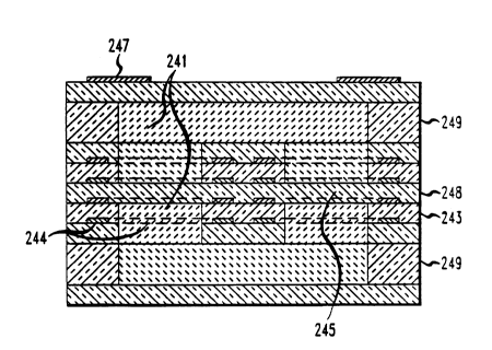
A cross section of a magnetic component having a toroidal magnetic
structure with a built in non-magnetic gap in the m~nçtic fluxpath is shown in FIG.
24. The cross section cut in this view is in the X-Z plane. This arrangement is a
vertical structure in which the insert portions 241 are magnetic. The construction of
5 this structure is similar to that of the structure shown in FIGS. 3 and 4, except that
the central insulating non-m~gn-otic layer or layers 248 do not have a~~ Gs for
insertion of m~gnçtic m~tt-ri~l The m~netic path defined by the inserts 241 is
therefore in~ellupled by non-magnetic gaps 245, the length of which can be
controlled by the layer thicl~nes5 or number of layers comprising 248. The structure
10 thus con~titlltes a gapped magnetic stlucture. The layered in~ul~ting portions 243
and 248 of the structure have surface printed conductors 244 comprising the
windings of the magnetic component. The members 249 comprise inml~ting non-
m~nçtic tape layers and, like the structure of FIGS. 3 and 4, provide top and bottom
insulative layers and apertures containing portions of the magnetic inserts 241.15 Connector pads 247, provided on the top surface of the structure, are connected to
the conductors 244 through vias which are not shown in this view.
A composite magnetic component structure incorporating a magnetic E
core structure is shown in a cross section view in FIG. 25. This cross section view is
cut in the X-Y plane. The magnetic insert portions 251 are inserted in a~)el lures in
20 the layered non-m~gn~ti~ insulating portion 253 and are the core structure that
provides the m~gnçtic path for flux. The conductors 254 are printed on the layers of
non-magnetic material 253. The vias 255 provide interlayer interconnections, andvias 256 are part of the conducting path connecting conductors of the bottom layer
with the connector pads on the top surface. Unlike conventional E core structures
25 which are comprised of two core halves mated together, the E core structure of FIG.
25 has a magnetic path uninterrupted by mating surfaces. Thus, the effective
permeability of the core equals the material permeability. This provides for a
significant pelrollllallce advantage over conventional E core structures wherein the
unavoidable non-vanishing air gaps at the making surfaces result in effective
30 permeabilities that can be typically as low as 50% of the material permeability. This
perform~nce advantage for magnetic co~ )onents constructed according to the
principles of the invention applies also to all the subsequently described magnetic
components that incorporate ungapped core structures.
A cross section in the X-Z plane of a magnetic component having an E
35 core structure with a built in gap is disclosed in FIG. 26. The printed conductors 264
forming the windings are printed on selected individual layers of the insulating non-
2~67a~8
.
- 14-
m~gnetic layers 263. The non-magnetic gap 265 occurs in the center leg of the E
core portion 261 of the structure. The conductors 264 are connected, via vias (not
shown) to the connector pads 268 printed on the top of the structure.
A cross section of a magnetic component incorporating a pot core
5 structure, embodying the principles of the invention, is shown in FIG. 27. This cross
section is taken in the X-Y plane. The printed conductors 274 comprising the
windings are printed on selected layers of the insulating non-m~n~,tie layers 273.
The magnetic m~t~,ri~l 271 is inserted into apGl LU1GS of the structure to form the pot
core configuration. The conductors of dirrGlGnt layers are connected by the vias 275.
A magnetic component having gapped pot core structure is shown in
FIG. 28 with the cross section taken in the X-Z plane. The non-magnetic gap 281 is
formed in the central leg of the magnetic m~teri~l 282 forming the core structure.
The conductors 283 forming the windings are printed on selected layers of the
in.~ ting non-magnetic m~teri~l 284 forming the structure. Connector pads 286 are
15 printed on the top surface of the structure and are connected to the c-n~ ctors 283
via vias (not shown).
The cross section of an alternative version of a magnetic component
incorporating gapped toroidal magnetic structure is shown in FIG. 29. The cross
section is taken in the X-Y plane and shows the vias 296 used in conjunction with
20 printed conductors 297 (shown schem~tie~lly) printed on in~nl~ting non-magnetic
layers (not shown) to form the magnetic device windings. These vias 296 are formed
in the insul~ting non-magnetic insert portions 294 (via carriers) of the structure.
Non-magnetic gaps 293 appear between the two halves of the m~gnetic core m~terisll
291. The gaps also contain in~ul~ting non-magnetic inserts to ensure conr~lllal
25 ~hrink~ge.
An ~ltern~tive magnetic component having an E core structure is shown
in an X-Z plane cross section in FM. 30. It has conducting vias 306 formed in the
insulating non-magnetic layers 309 and inserted via calTiers 303. These vias
lGpl~sellt a portion of the device winding. The windings are completed with the
30 printed conductors 304 printed on the in~ ting material layers 309. The m~netic
layers 301 form the magnetic path in the structure. Connector pads 308 are provided
on the top surface of the structure.
A magnetic component incorporating a gapped E core structure is shown
in a cross section view in the X-Y plane in the FIG. 31. This structure utilizes the
35 vias 315 in the insulating non-magnetic inserts 316 and printed conductors 317
(shown schem:~tic~lly) printed on insulating non-magnetic layers (not shown) to
20~7~08
form the device win~lings. A gap 313 appears in the center leg of the m~neti~
material layers 314 forming the E core. The gap also contains an in~ ting non-
m~netic insert to ensure confo~ al shrinkage.
An open structure magnetic device (i.e. a device with an open magnetic
5 circuit) with the cross section taken in the X-Z plane is shown in FIG. 32.
Conductor windings 321 are printed on several selected layers of the in~ ting non-
m~gnt tic m~teri~l 322 to encircle a central core formed of layers of m~.~netic
material 323. Connector pads 325 are printed on the top surface of the structure. It
is important for the m~teri~l 322 to be non-magnetic for this circuit to function as an
10 open magnetic circuit. This applies also to the device of FIG. 33 described below.
An ~ltern~tive open structure magnetic device with the cross section
taken in the X-Y plane is shown in FIG. 33. Conductor windings are formed from
the printed conductors 333 (shown schematically) printed on insulating non-
magnetic layers (not shown) and the vias 334, which are contained in the insulating
15 non-magnetic via carriers 335. The windings surround the layered m~gn~tiC m~teri~l
336.
While many specific implementations of the invention have been shown
it is to be understood that many variations of this invention may be imp!çmented by
those skilled in the art without departing from the spirit and scope of the invention.