Note: Descriptions are shown in the official language in which they were submitted.
2067025
SEI 92-3
1 Title of the Invention
MULTI-STAGE AMPLIFIER DEVICE AND METHOD FOR
PRODUCING THE SAME
Back round of the Invention
(Field of the Invention)
This invention relates to a multi-stage amplifier
device and a method for producing the same, which is
used as a microwave low-noise amplifier for a
satellite-broadcast receiving converter, a wideband
amplifier for a measuring equipment or the like.
(Related Background Art)
In association with a recent rapid development of
an information net work system, a satellite
communication and broadcasting system have been
intensively required, and a frequency band of the
system has been also required to be further shifted to
a higher one. In order to satisfy these requirements,
various circuit elements such as a field effect
transistor, etc. which can be operated in a high
frequency band have been studied and developed. A
Schottky-barrier type electric field ef~ect transistor
(MESFET) formed of compound semiconductor has been used
such as a field effect transistor for high frequency
band. Especially GaAs compound semiconductor
206702~
SEI 9Z-3
1 transistor has been employed because it can break-
through a limitation in characteristics of an Si
bipolar transistor. In addition, in order to satis~y
various requirements such as miniaturization, low-cost
and high performance for a system, integration of a
first-stage amplifying portion of a down-converter has
been recently constructed as MMIC (Microwave
Monolithic Integrated Circuit).
In an MMIC low-noise amplifier used in a microwave
band, amplifiers at all stages thereof have been
conventionally formed of the same FET (Field Effect
Transistor), that is, the front and rear stages of the
MMIC amplifier are not designed so as to have different
FET constructions. In order to attain a low noise
amplifier, an FET having a gate structure which is
designed in self-alignment with a source and a drain
has been practically used.
In order to reduce a noise figure of a FET, it is
important to increase transfer conductance gm of the
FET and lower gate-source capacitance Cgs of the FET,
or to lower source resistance Rs. In order to increase
the transfer conductance gm, and to lower the gate-
source capacitance Cgs, the gate length of the FET is
mainly required to be set to 0.25 ~m or less. ~n the
other hand, in order to lower the source resistance Rs,
2067025
SEI 92-3
1 it is mainly required to approach an n+ contact region
to the gate as near as possible. If the gate is formed
in a self-alignment structure, the gate length could be
shortened, and the n contact region and the gate could
be formed in such a manner that an interval
therebetween is remarkably shortened with high
reproducibility irrespective of alignment accuracy of
an exposing device. The lowering of the source
resistance Rs is also effective for the increase of gm
and the lowering o+ an equivalent noise resistance Rn.
As described above, in the conventional MMIC low-
noise amplifier used in the microwave band, the
amplifiers at all stages are designed using FETs having
the self-alignment structure.
However, when the gate is formed in the self-
alignment structure as described above, an n contact
region at the drain side is also nearly approached to
the gate, like the n+ contact region at the source side,
so that a drain-gate breakdown voltage (a durable
maximum voltage to be applied between the drain and the
gate) will be lowered.
The MMIC amplifier has a large gain with one chip
having a multistage connection. Therefore, even if an
input signal power is weak at the first stage, the
amplitude of the signal is more intensified as it
206702~
SEI 92-3
1 proceeds to the subsequent stages. Therefore, there
frequently occurs a case where a voltage exceeding the
drain-gate breakdown voltage of the FET is
unintentionally applied between the drain and the gate
of the FET, and the FET is damaged. Moreover, in such a
type of amplifier, a parameter representing linearity
of an amplifier, such as ldB compression output power
or IM3 intercept point, is regarded as an important
index value, and a higher index value represents higher
performance of the amplifier. If the voltage exceeding
the drain-gate breakdown voltage of the FET is applied
betwe0n the drain and the gate of the FET as described
above, the linearity of the amplifier would be
deteriorated, and values of the ldB compression output
power and the IM3 intercept point would be reduced.
Summar~ of the Invention
An object of this invention is to provide a
multistage amplifier device having a low noise figure,
high ldB compression output power and IM3 intercept
point, and a large gain.
In order to attain the above object, the
multistage amplifier device according to one aspect of
this invention includes plural amplifiers which are
formed on the same semiconductor substrate, an active
2067025
SEI 92-3
1 element of an amplifier at the first stage or each of
active elements o+7 amplifiers at plural stages which
contain the first stage and exclude the last stage
being formed of a first MESFET, and each of active
elements of amplifiers at remaining stages being formed
of a second MESFET. The first MESFET has a gate
structure in a self-alignment with a source and a drain
thereof, and the second MESFET has a gate electrode on
semiconductor layer sandwiched between a source high
impurity density region and a drain high impurity
density region, the gate electrode having one edge
portion at a source side which is overlapped through an
insulating layer with the source high impurity density
region, and having the other edge portion at a drain
side which does not expand to the drain high impurity
density region.
Since the total noise figure is mainly dependent
on the noise figure of the amplifier at the first
stage, the amplifiers at the front stages containing
the first stage are formed of the first MESFETs having
high transfer conductance gm and low noise figure. On
the other hand, in the second MESFET the gate
electrode is deviated to the source side, and a
sufficient interval is kept between the gate electrode
and the drain n region, so that a large drain-gain
2067025
SEI 92-3
1 breakdown voltage can be obtained. However, the high
impurity density region (n contact region) at the drain
side is disposed far away from the gate electrode.
Accordingly, a depletion region expands from a channel
to the drain side, and the transfer conductance gm is
liable to be reduced because of long effective gate
length. Therefore, the second MESFET having this
construction is inferior in noise performance to the
first MESFET having a gate which is designed in the
ordinary self-alignment structure.
In view of the above, in this invention the
amplifier at only the first stage, or the amplifiers at
some stages containing the first amplifiers and a
proper number of subsequent amplifiers are formed of
the first MESFETs each including a gate having the
ordinary self-alignment structure in which both edge
portions of the gate are overlapped with the source and
the drain, and the amplifiers at the remaining stqges
are formed of the second MESFET including a gate having
a self-alignment structure at only the source side.
With this arrangement, "the low noise performance" and
"the high breakdown voltage" can be simultaneously
obtained.
According to the multistage amplifier device of
another aspect of this invention, the first MESFET is
206702~
SEI 92-3
1 formed on a GaAs epitaxial layer having a first
sectional structure and the second MESFET is formed on
a GaAs epitaxial layer having a second sectional
structure. The GaAs epitaxial layer having the first
sectional structure is designed in a pulse dope
structure which comprises a channel layer having a high
carrier density and a cap layer having low carrier
density on the channel layer, and the GaAs epitaxial
layer having the second sectional structure has a
channel layer having high carrier density, and a cap
layer having low carrier density on the channel layer,
the cap layer having a multilayer structure and an
impurity doping layer as an intermediate layer.
The first MESFET has excellent noise performance,
but it also would be provided with low phase-noise
performance if it is formed of the GaAs epitaxial layer
having the first sectional structure. Therefore, the
MESFET thus constructed is more preferably used as a
constituent of a low-noise amplifier.
In the second MESFET the gate electrode is
deviated to the source side, and a constant interval is
kept between the gate electrode and the drain, so that
a large drain-gain breakdown voltage can be obtained.
However, the high impurity density region (n contact
region) at the drain side is disposed far away from the
206702~
SEI 92-3
1 gate electrode, a depletion region expands from a
channel to the drain side, and the transfer conductance
gm is liable to be reduced because of long effective
gate length. However, if the second MESFET is formed
of the GaAs epitaxial layer having the second sectional
structure, the effective gate length would be prevented
from being long by the impurity doping layer in the cap
layer, and the drain breakdown voltage could be
increased without the lowering of gm. In order to
obtain a high output power, it is required to make a
threshold voltage Vth of the FET low, and as the
result, the thickness of the high density pulse dope
layer serving as the channel layer should be over a
predetermined value. However, in view of the low-noise
performance, the thickness of the channel layer is
required to be thin for a good performance, and thus
the FET having this structure is unsuitable for the
amplifier at the first stage.
In view of the above, in this invention, the
amplifier at only the first stage, or the amplifiers at
some stages containing the first amplifiers and a
proper number of subsequent amplifiers are formed of
the first MESFET having the GaAs epitaxial layer having
the first sectional structure, and the amplifiers at
the remaining stages are formed of the second MESFET
2Q6702~
SEI 92-3
1 having the GaAs epitaxial layer having the second
sectional structure. With this arrangement, "the low
noise performance" and "the high breakdown voltage" can
be simultaneously obtained.
A method according to the present invention, for
producing the multistage amplifier device having the
above structure comprises; the steps of superposedly
forming the GaAs epitaxial layer with the second
sectional structure on the GaAs epitaxial layer having
the first sectional structure, and thereafter,
selectively removing the GaAs epitaxial layer with the
second sectional epitaxial structure by etching
process.
The two kinds of the epitaxial structures (layers)
may be selectively grown without the etching process.
However, this technique has a problem which is
difficult to be overcome in a growth technique and a
process technique, and thus it is more easily performed
in a manufacturing technique that the GaAs epitaxial
layer having the second sectional structure is
superposedly formed on the GaAs epitaxial layer having
the first sectional structure, and then the GaAs
epitaxial layer having the second sectional structure
is selectively removed by an etching process.
In place of the above producing method, the
206702~
SEI ~2-3
1 following producing method which is inverse to the
above method may be adopted. That is, the GaAs
epitaxial layer having the first sectional structure is
superposedly formed on the GaAs epitaxial layer having
the second sectional structure, and then the GaAs
epitaxial layer having the first sectional layer is
selectively removed by the etching process. In this
case, the performance of the FET used at the first
stage amplifier is most important, and thus the
epitaxial layer having the first sectional structure
used at the first stage is preferably formed below the
epitaxial layer having the second sectional structure
in view of the problem caused by leak current flowing
into the substrate.
The present invention will become more fully
understood from the detailed description given
hereinbelow and the accompanying drawings which are
given by way of illustration only, and thus are not to
be considered as limiting the present invention.
Further scope of applicability of the present
invention will become apparent from the detailed
description given hereinafter. However, it should be
understood that the detailed description and specific
examples, while indicating preferred embodiments of the
invention, are given by way of illustration only, since
2067~25~
SEI 92-3
1 various changes and modifications within the spirit and
scope of the invention will become apparent to those
skilled in the art form this detailed description.
- Brief DescriPtion of the Drawin~s
Fig. 1 is a sectional view of a MESFET
constituting an amplifier at each stage of a first
embodiment of the multistage amplifier device of this
invention;
Fig. 2 is an equivalent circuit diagram of the
multistage amplifier device as shown in Fig. 1;
Fig. 3 is an enlarged sectional view of a gate
portion of MESFET la or lb;
Fig. 4 is an enlarged sectional view of a gate
portion o* MESFET lc or ld;
Fig. 5 is a sectional view of a MESFET
constituting an amplifier at each stage o~ a second
embodiment of the multistage amplifier device of this
invention; and
Fig. 6 is an equivalent circuit diagram of the
multistage amplifier device as shown in Fig. 5.
.
Description of the Preferred Embodiment
Preferred embodiments according to this invention
will be described hereunder with reference to the
!
2067~25
SEI gz-3
1 accompanying drawings.
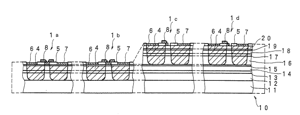
A first embodiment of this invention will be first
described with reference to Figs. 1 to 4.
As is apparent from Fig. 2, this embodiment is a
four-stage cascade-connected type MMIC multi-stage
amplifier comprising four amplifiers lOOa to lOOd, and
various elements including FETs la to ld are formed on
a GaAs substrate 10.
The GaAs substrate 10 has a double epitaxial
structure. The first epitaxial structure comprises an
undoped GaAs layer (buffer layer) 12, an Si-doped GaAs
layer (channel layer) 13 and an undoped GaAs layer (cap
layer) 14 which are continuously grown on a semi-
insulating GaAs substrate 11. The second epitaxial
structure comprises, an undoped GaAs layer (buffer)
layer 16, an Si doped GaAs layer (channel layer) 17, an
undoped GaAs layer (cap layer) 18, an Si doped GaAs
layer 19 and an undoped GaAs layer (cap layer~ 20 which
are formed on the semi-insulating GaAs substrate 11
having the layers 12, 13 and 14 as described above.
The undoped GaAs layer 12 is formed in p-density
of 2 X lO15cm3 and thickness of 10000 A, the Si doped
GaAs layer 13 is formed in doping density of 4 X 1018cm3
and thickness of 100 A, and the undoped GaAs layer 14
is formed in n-density below 1 X 1015cm3 and thickness
12
206702~
SEI 92-3
1 of 300 A. In addition, the undoped GaAs layer (buffer
layer) 16 is formed in p-density of 2.5 X lO15cm3 and
thickness of 10000 A, the Si doped GaAs layer (channel
layer) 17 is formed in doping density of 4 X 1018cm3 and
thickness of 200 A, the undoped GaAs layer 18 is formed
in n-density below 1 X lO15cm3 and thickness of 150 A,
the Si doped GaAs layer 19 is formed in doping density
of 4 X 1013cm3 and thickness o~ 50 A, and the undoped
GaAs layer 20 is formed in n-density below 1 X lOl5cm3
and thickness of 200 A.
After the double epitaxial structure as described
above is formed, an upper portion of the structure
which expands from the undoped GaAs layer 16 to the
undoped GaAs layer 20 is selectively removed by an
etching process. In this case, the etching amount or
depth is slightly equal to l~m + several angstroms, and
thus it is dif~icult to accurately control the etching
amount on the basis of only a time-control. In view of
the above, for example, an AlGaAs thin layer 15 is
provided as a etch stop layer, and the selective
etching process of the GaAs layer can be sufficiently
assured by a wet etching process using an etchant
having a selective etching capability. As a result,
the upper portion can be selectively etched with high
controllability using the above wet etching process.
206702~
SEI 92-3
1 As described above, since the AlGaAs thin layer 15 is
provided as the etch stop layer for the etching process
for selectively removing the upper portion, the AlGaAs
thin layer 15 is required to be sufficiently thin to
the extent that it has no affection on the operation of
the FET.
Recessed portion is formed in the above etching
process. Ampli~iers lOOa and lOOb which are
respectively the first and second stages are formed in
the recessed portions, and amplifiers lOOc and lOOd
which are respectively third and fourth stage are
formed in the remaining portion except for the recessed
portion.
In this case, each of FETs la and lb constituting
the amplifiers lOOa and lOOb at the first and second
stages includes a gate having the ordinary self-
alignment structure, but each of FETs lc and ld
constituting the amplifiers lOOc and lOOd includes a
gate having "the self-alignment structure at only the
source side".
All of the FETs la, lb, lc and ld commonly have
the following basic construction. Source and drain
high impurity density regions 4 (portions indicated by
oblique lines) are disposed on the GaAs substrate 10 by
ion-implantation method, a part of each of the source
14
206702~
SEI 9Z-3
1 and drain high impurity density regions 4 is covered by
an insulating film 5, source and drain electrodes 6 and
7 are formed at exposed portions of the regions 4 in
which the unslating film 5 is removed, and a gate
electrode 8 is formed on a semiconductor layer
sandwiched between the source and drain high impurity
density regions 4. However, there is the following
different point in construction between the FETs la,
lb, lc and ld: each of the gate electrodes 8 of the
FETs la and lb is designed such that both edge
portions of the gate electrode 8 at the source and
drain sides are superposedly provided through the
insulating films 5 on the source and drain high
impurity density regions 4 while each of the gate
electrodes 8 of the FETs lc and ld is designed such
that one edge portion thereof at the source side is
superposedly provided through the insulating film 5 on
the high impurity density region 4, but the other edge
portion at the drain side does not expand to the high
impurity density region 4.
Fig. 3 is an enlarged sectional view of a gate
portion of the FET la or lb, and Fig. 4 is an enlarged
sectional view of a gate portion of the FET lc or ld.
Each gate electrode of the FETs la to ld has a gate
metal length Lm of about 0.5 to 1 ~m, but the effective
2067025
SEI 92-3
1 length thereof corresponds to the length of a portion
excluding the overlapped portion on the insulating ~ilm
5. The gate length Lgl of the FET la or lb is about
0.3 to 0.5 ~m, and the gate length Lg2 of the FET lc or
ld is approximately about 0.2 ~m. In the gate portions
of the FETs lc and ld, the length Ln of a part where no
gate electrode is formed is about 1.5 ~m.
These FETs can be formed in a lump in the
following ordinary process for manufacturing a FET
including a gate having the self-alignment structure.
That is, a dummy gate is formed on the semiconductor
layer in the gate region to form the high impurity
density region 4 using the dummy gate as a mask, and an
inversion pattern of the dummy gate is formed using the
insulating film 5. A part of the pattern is removed to
expose a part of the high impurity density region 4.
The source and drain electrodes 6 and 7 are formed on
the exposed portions of the high impurity density
region 4, and the gate electrode 8 is formed on the
gate region. In this case, the opening of the mask used
in the patterning process of the gate electrode 8 is
designed so as to be disposed at such a suitable
position that in the FETs la and lb both of the edge
portions of each gate electrode at the source and
drain sides cover at least a part of each of the
16
206702~
SEI 92-3
1 source and drain high impurity density regions 4 while
in the FETs lc and ld the edge portion of each gate
electrode at the source side covers at least a part of
the source high impurity density region 4, but the
other edge portion at the drain side does not cover or
expand to the drain high impurity density region 4.
The FETs la and lb at the front stages (first and
second stages) include gates having the ordinary self-
alignment structure, so that the transfer conductance
gm is high and the noise figure is low. In addition,
the channel layer 13 is formed as the pulse dope layer
in suitable depth from the surface, in high carrier
density and in thickness of 100 ~, so that the phase
noise is also low. The total noise figure (NFT) of the
multistage amplifier is represented by the following
equation~
T Fl + ~NF2 l)/Gl + (NF3-1)/GlG2 + -- + (NF -
1)/Glg2Gn-l
Here, NFT represents total noise figure; NFl, noise
figure at the first stage; NF2, noise figure at the
second stage; ...; NFn, noise figure at the nth-stage;
Gl, gain at the first stage; G2, gain at the second
stage; ...; Gnl~ gain at the (n-l)th stage.
As is apparent from the above equation, the total
noise figure of the multistage amplifier is mainly
17
2067025
SEI 92-3
1 dependent on the noise figure of the amplifier at the
first stage. Therefore, the multistage amplifier device
of this embodiment which uses the amplifiers having low
noise figure at the first and second stages has a
sufficiently low noise figure.
In addition, a suitable distance Ln is kept between
the gate electrode 8 and the drain high impurity
density region in the FETs lc and ld which are used for
the amplifiers at the third and fourth stages, so that
the drain-gate breakdown voltage can be set to a large
value. As described above, since the large drain-gate
breakdown voltage is set in the FETs of the amplifiers
at the rear (third and fourth) stages where the signal
amplitude is intensified, the values of the ldB
compression output power and the intercept point can be
increased while the linearity of the multi-stage
amplifier can be maintained. In addition, since the
FETs lc and ld are formed on the epitaxial layer having
the structure that the cap layer having the multi-layer
structure is formed on the channel layer 17 and the
impurity doping layer l9 is provided as an intermediate
layer of the cap layer, expansion of the depletion
region due to a surface level between the gate
electrode 8 and the drain high impurity density region
4 can be prevented to the extent that the depletion
18
206702~
SEI 92-3
1 region does not expand to the channel layer 17. The
carrier density and thickness of the impurity doping
layer 19 of the cap layer of the GaAs epitaxial layer
may be set to such values that a bottom portion of the
surface depletion region due to the surface level is
disposed between the impurity doping layer 19 and the
channel layer 17. Therefore, the high gm can be
obtained keeping the sufficient distance between the
gate and the drain for high breakdown voltage.
As a method of increasing the drain-gate breakdown
voltage are proposed a recess system using a rPcess
structure, and a "slant ion-implantation method" in
which ion implantation to the n+ region is carried out
in a slant direction from the source to the drain in
place of a vertical ion-implantation in which an ion
implantation is carried out from the top of the gate to
the n region. Since, the recess system, that is, the
gate region is removed by the etching process has
difficulty in reproducibility and controllability of
the etching process, the gate electrode can not be
obtained with high reproducibility and uniformity.
Therefore, the FET structure of this system is
unsuitable for the MMIC. On the other hand, in the
slant ion-implantation method, the n region can be
+ormed in the self-alignment structure, and the
19
206702~
SEI 92-3
1 interval between the n+ region and the gate can be
designed asymmetrically at the source and drain sides,
so that there is a possibility that "low noise
performance" and "high breakdown voltage" can be
simultaneously obtained. However, in this method, the
ion is unintentionally implanted into the channel layer
under the gate portion due to the slant ion
implantation. As a result, the carrier number is
increased and the drain conductance gm is increased,
but the gate capacitance Cgs is increased, so that it
is difficult to obtain "low noise performance".
Rather, the vertical ion-implantation from the top of
the gate is more excellent in low-noise performance
than the slant ion-implantation method.
Accordingly, the "low-noise performance" and the
"high-output power" can be simultaneously obtained by
the following construction. The FET at the front
stages (first and second stages) are selectively formed
by the vertical ion-implantation method to design the
FETs at these stages in a structure suitable for the
low-noise performance, while the FETs at the rear
stages (third and fourth stages) are selectively formed
by the slant ion-implantation method to design the FETS
at these stages in a structure suitable for the high
breakdown voltage. However, in order to selectively
2067025
SEI 92-3
1 form the front stages by the vertical ion-implantation
method and selectively form the rear stages by the
slant ion-implantation method, the number of masks must
be increased, and the processes must be complicated.
Therefore, this technique is an unrealistic one.
A second embodiment of this invention will be next
described with reference to Figs. 5 and 6.
Fig. 5 is a sectional structure of an FET portion
constituting an amplifier at each stage of the
multistage amplifier, and Fig. 6 is an equivalent
circuit diagram of the multistage amplifier.
As is apparent from Fig. 6, this embodiment is an
example of the MMIC amplifier having the four-stage
cascade-connected structure like the first embodiment,
and various elements containing FETs 41 to 44 are
formed on the semi-insulating GaAs substrate. Each of
the FETs 41 to 44 commonly has the same basic
construction. That is, an active layer 32 and source
and drain high impurity density regions 34 which are
disposed so as to sandwich the active layer 32, are
formed on a GaAs substrate 31, respective parts (at
the sides adjacent to the active layer 32) of the
source and drain high impurity density regions 34 are
covered by an insulating film 35, exposed portions of
the source and drain high impurity density regions 35
2~6702~
SEI 92-3
1 are formed with source and drain electrodes 36 and 37,
and an gate electrode 38 is formed on the active layer
32.
As shown in Fig. 5, the FETs 41 and 42
constituting the amplifiers 401 and 402 at the first
and second stages are designed so as to include a gate
having the ordinary self-alignment structure, but the
FETs 43 and 44 constituting the amplifiers 403 and 404
at the third and fourth stages are designed so as to
include a gate having the self-alignment structure at
only the source side. That is, the gate structure of
the FETs 41 and 42 used for the amplifiers at the first
and second stages has the same shape and size as the
FETs la and lb of the first embodiment, and the gate
structure of the FETs 43 and 44 used for the amplifiers
at the third and fourth stages have the same as the
FETs lc and ld.
There~ore, in this embodiment, the transfer
conductance gm of the FETs 41 and 42 has a large value,
and the noise figures of the amplifier 401 and 402 are
low. In addition, the gate-drain breakdown voltage of
the FETs 43 and 44 is high. As a result, the multistage
amplifier of this embodiment has low noise figure and
high gain as a whole.
In the first and second embodiments as described
206702~
SEI 92-3
1 above, the amplifiers at the first and second stages
are formed of FETs including the gate having the
ordinary self-alignment structure, and the amplifiers
at the third and fourth stages are formed of the FETs
including the gate having the self-alignment structure
at only the source side. However, this invention is
not limited to the four-stage cascade-connected
structure. In addition, the respective numbers of the
stages where the FETs including gates having the
ordinary self-alignment structure are used and where
the FETs including gates having the self-alignment
structure at only the source side are used, are
determined in accordance with various factors such as
the gain of the amplifier, the amplitude of an input
signal, etc., and thus the optimum construction of the
multistage amplifying circuit is variable in accordance
with these factors.
From the invention thus described, it will be
obvious that the invention may be varied in many ways.
Such variations are not to be regarded as a departure
from the spirit and scope of the invention~ and all
such modifications as would be obvious to one skilled
in the art are intended *o be included within the scope
of the following claims.