Note: Descriptions are shown in the official language in which they were submitted.
2067202
SPECIFICATION
Title of Invention
SUR~E ABSORBING COMPONENT TO PROTECT
FROM OVERVOLTAGE AND OVERCURRENT
FIELD OF ART
The present invention relates to a surge absorbing component
for protecting semiconductor circuit or a telephone line from a
lightening surge and overvoltage or overcurrent, which can avoid
firing and overheat of the circuit substrate, even when
overvoltage or overcurrent is applied to the circuit.
BA~KGROUNr) OF THE ART
A surge absorber is to protect an equipment such as a
communication line, e.g. a telephone line for telephone and
telecopier, and a line for a cable television and a cable radio
and the like, as well as a device, e.g. semiconduçtor device,
from a lightening surge.
A protection function of the surge absorber is to protect a
communication device connecting communication lines when the
communication line interconnects the source line to load
overcurrent or overvoltage on the line, which will heat the
breaker fuse wire so as to melt the wire, thereby opening the
circuit to protect the equipment from the overcurrent and
overvoltage. In the conventional surge absorber having function to
protect from overcurrent and overvoltage, a low melting point
metal wire is only surrounding the surge absorber within inorganic
material bousing. Connecting terminals are provided at the both of
the ends of the inorganic material housing of the surge absorber.
2~67202
~ urther, there have been published Japanese Patent
Publication No. 63-205026/1988 and Japanese Patent Application No.
~1-152703 as measures to resolve the case where the short-circuit
with source occurs, which disclose a method of preventing
overheat and fire of a surge absorbing element by contacting a
low- melting point metal wire with the surface of a microgap surge
absorbing element so that the heat generated by overvoltage or
overcurrent charged in the surge absorbing element will melt
easily and rapidly the low melting point wire, thereby, making to
open the circuit. The structure of mounting the low melting point
metal wire on the surface of the surge absorbing element is housed
within a case of inorganic material.
In this structure, a temperature fuse or low melting point metal
wire is mounted in contact with the surface of the surge absorbing
element can protect the surge absorbing element and the equipment
to be connected. The heat generated on the surface thereof by the
overheat of the surge absorbing element will melt the fuse or low
melting point metal wire, making to open the circuit. Therefore,
the conventional structure will require complete melting down of
the temperature fuse or the low melting point metal wire so as to
made open the circuit. It takes relatively longer time to attain
complete melting down of the fuse or the low melting point metal
wire.
Such component of the conventional structure has three or four
external terminals, and one or two terminals among these one are
in form of wire, and then, the connecting position is unstable,
and not easy to be assembled. FurtherJ a cover glass tube which is
disclosed in Japanese Patent Publication No. 63-205026/1988, will
be naked and directly in contact with a substrate when assembled
20~72~
in the circuit. Therefore, when the overcurrent or overvoltage is
continuously applied to the component, the surge absorbing element
located within a hollow of a cover glass is heated and then the
low melting point metal wire is broken by the heat generated in
the surge absorbing element. The cover glass tube is heated
through such phenomenon, so that the substrate as assembled within
a hollow of cover glass is affected by such heat( exothemal and
generating smoke) and in some cases would be fired.
DISCLOSURE OF INVENTION
With the foregoing considerations in mind, the present
invention contemplates the provision of an improved surge
absorbing component
with shorter time of making open the circuit. ~or the contemplated
component, a metal with high stiffness modulus which has been
elastically deformed is used to be mounted on the electrodes or
the leads of the surge absorbing element, by using low melting
point metal wire, and then, the heat generated by application of
continuous overvoltage or overcurrent will melt the low melting
point metal connecting the stiff metal wire and the lead of the
element, and the metal wire with high stiffness which has been
deformed will be returned to original shape, and thereby leaving
rapidly the connection point (the lead of the element). Therefore,
the protective surge absorbing component with rapid response can
be attained, and then the safety of the surge absorbing component
can be improved. That is, the structure of the present invention
can enable to make open the circuit as soon as possible after the
low melting point metal is melt, because the metal wire with high
stiffness which has elastically deformed and fixed on the terminal
of the element will be returned mechanically and rapidly into
2~67202
original shape, by its elasticity, at the time when the low
melting point metal is melt by the heat generated by the surge
absorbing element when overvoltage or overcurrent is applied to.
"~ surge absorbing component" hereinafter means "an equipment
to avoid application of overvoltage and overcurrent by providing
a gap or microgap on a portion of conductive thin film, such that
discharge will occur through the gap or microgap, when overvoltage
higher than optical level is applied on the gap or microgap,
generating a branch flow for the overvoltage or overcurrent", and
in ordinal structure, the conductive film having the gap or the
microgap is enclosed and sealed in gas-charged tube. Therefore,
it can be called a gap or microgap surge absorbing element.
Hereinafter, "a surge absorbing component having protection
function" means "a network or system including a surge absorbing
element to protect a communication device connecting communication
lines when the communication line interconnects the source line,
with the combination with fuse and the other elements and
component, so as to prevent overheat and fire due to the
overcurrent or overvoltage on the line.
The resin base for the surge absorbing component can be
made from resin such as epoxy resin and poly butadien type resin.
Three terminal pins are mounted on the surface of the resin base.
The terminal pins have the diameter of 0.5 to 1.0 mm and the
length of about 10 mm. Further, the resin base has a structure on
which an inorganic housing or cover glass tube can be fixed with
its margin. Within the housing, a gap or microgap surge absorbing
element, a metal wire with high stiffness which has been
elastically deformed, and connected and fixed between the terminal
2~67202
of the element and the lead pin, the lead wires of the element
are provided in enough space. The lead pins will fix the element
and the deformed metal wire with high stiffness is fixed on one of
the terminals or electrodes of tlle element, through low melting
point metal.
The housing is fixed with resin, such that the heat from
the gap or microgap surge absorbing device is prevented from
conducting to the outside of the component. The metal wire with
high stiffness which has been elastically deformed and each of
the lead wires are fixed
by binding or spot welding on each of the lead pins mounted on
the resin base.
Therefore, the influence of the heat can be restrained within
the space of the surge absorbing component of the function to
protect from the overvoltage and overcurrent, and does not affect
the outside of the component.
The efficiency of assembling the inventive surge absorbing
component can be improved by using a predetermined number of the
lead pins which are previously mounted or fixed on the resin base
so as to assemble or fix the surge absorbing element within the
component.
SIMPLE DESCRIPTION OF DR~WINGS
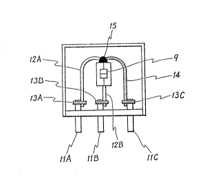
FIG. 1 shows schematically a sectional view of a surge
absorbing component according to the present invention.
FICG 2 shows schematically a circuit for a surge absorbing
component according to the present invention.
~72~
BEST MODE l~OR CAl~RYING OUT THE INVENTION
FIG. 1 shows schematically a sectional view of a surge
absorbing component having protection function according to the
present invention. There are provided a surge absorbing element 9,
arranged in hollowed resin case 8 and on a resin base 10 to which
the surge absorbing element 9 is mounted, and three lead pins
11A, llB and llC mounted on the resin base 10, and respective
lead wires 1 2A and 1 2B connected to each of the terminals of the
surge absorbing element 9, a phosphor bronze wire 14 which has
been elastically deformed mounted on one of the terminals of the
surge absorbing element 9 through solder 15.
The inventive surge absorbing component having protection
function utilizes this feature of the metal wire with high
stiffness modulus which has been elastically deformed, and which
mounts the terminal or lead wire of the surge absorbing element.
When the surge absorbing element is heated by application of
overvoltage or overcurrent, the metal wire with high stiffness
can be returned immediately after the low melting metal is melt,
and thereby enabling rapidly making open the circuit, and at the
same time, the elastic deformation of the metal wire with high
stiffness will function to enforce to leave or to
open the circuit by mechanical force.
The surge absorbing component having protection function
can be used in a connector with a telephone line, a telecopier
machine, and a telephone exchanging machine, in order to protect
from a surge and overvoltage and overcurrent.
The present invention is further illustrated by the following
2~67202
example, but should not be interpreted for the limitation of the
invention.
EXAMPLE
FIG. 1 shows in sectional view a structure of an embodiment of
the a surge absorbing component having protection function of the
present invention.
Terminal pins 11~, llB and llC are mounted on a resin base 10,
and then, a microgap surge absorbing element 9 (direct discharge
initiating voltage = 300 V) is mounted by one of lead wire 12A
which has been bent as shown in the drawings, and the other one of
lead wire 12B, respective lead wires 12A and 12B are mounted on
each of lead pins llA and llB through each of binders 13A and 13B
so as to connect electrically, and fixed as shown in FIG. 1.
Then, a phosphorus bronze wire 14 is used as a metal wire with
high stiffness, to connect the lead pin llC by means of a binder
13C, and the other end of the phosphorus bronze wire 14 is bent by
force as shown in FIG. 1, and fixed on the lead wire 12A of a
microgap surge absorbing element 9, i.e. fixed on the terminal of
the surge absorbing element by means of solder 15 as a low melting
point metal, thereby forming electrical connection, and fixed.
Further, the whole structure is surrounded by a resin cover 16.
Then, the surge absorbing component having protection function
can be obtained as shown FIG. 1, with three terminals.
The inventive surge absorbing component having protection
function is assembled and is cosmected as shown in the circuit
diagram of FIG. 2, a microgap surge absorbing element 9 and a
metal wire with high stiffness 14 are assembled, and the telephone
2~7202
line 3 is connected so as to protect an equipment 2 from surge.
Further, each of terminals llA, llB and llC are positioned as
shown in FIG. 2.
The above assembled surge absorbing component having protection
function was tested by charging overvoltage, and the reference
product was tested similarly. The result is described as below
table 1.
Herein, the reference product has the above-mentioned
conventional structure, i.e. a temperature fuse is mounted around
the surface of the gap or microgap surge absorbing element, and
will be melt down when heated, so that the protection function is
provided.
Table 1
Applied Voltage AC 600V AC 6QOV AC 600V AC 600V AC 600V AC 600V
Applied Current 40 A 7 A 2.2 A 1 A 0.5 A 0.25 A
Result
Time of opening
the circuit
Inventive 15-250.2-0.4 1-2 2-4 3-5 3-10
Product mm seconds
Reference 15-25 0.2-0.4 3-6 6-10 10-30 20-50
mm seconds
It is apparent from Table 1 that the inventive product
evidences significant improvement of the performance in range of
lower current applied.
INDUSTRIAL UTILIZATION
2~672Q2
The inventive surge absorbing component for protecting a
communication line from overvoltage or overcurrent will provide
relatively shorter time for making open the circuit in comparison
with the reference product, by using a metal wire with high
s-tiffness which has been elastically deformed, and therefore,
enabling to discontinue rapidly the loading of overvoltage or
overcurrent.
The metal wire with high stiffness which has been elastically
deformed can be returned mechanically immediately after the
overvoltage or overcurrent is applied, and then, $he circuit for
the surge absorbing element is rapidly made to be open so as to
protect the equipment.
Therefore, the inventive surge absorbing component with
protection function can protect the equipment such as a telephone,
telecopier, and telephone exchanger being connected to the line,
from surge and overvoltage and overcurrent, then improving the
operation performance of the surge absorbing component having
protection function.
1 0