Note: Descriptions are shown in the official language in which they were submitted.
CA 02067418 1998-01-16
_
YO9-9 1 -093
FRAME BU~;~ ORGANIZATION AND CONTROL FORREAL-TIM:E IMAGE
DECOMPRESSION
FIELD OF THE INVENTION:
This invention relates to high performance display systems, and more particularly, to a
frame buffer for use in such a high pelÇu-lllallce display system wherein image
decompression is accomplished in real time.
BACKGROUND OF THE rNVENTION:
Scientific vi~ li7~tion helps users better understand the large quantities ûf data with
which they are dealing. These vi~ li7.~tions are typically computed on a large super
computers and are sent to user wolk~lalions for viewing over a high speed network. One
powerful technique for vi~ li7.~tion is the use of motion to augment a user's
understanding of the data. By creating animations which show various surfaces of the
data being viewed and displaying them as a smooth motion sequence, more information
about the data being studied can be conveyed.
As the user's display resolution increases, it is increasingly difficult to send enough data
over the network to provide the smooth motion required. Even with a high bandwidth
communication network, transmitting enough data for smooth motion (30 frames persecond or higher) is difficult without the use of some form of compression and
decompression. If each pixel is represented by 24 bits, such that each 8 bit byte represents
a color, then it can be shown that the data throughput required to show motion is T
=3HresVresFref bytes per second, where T is throughput in bytes per second, Hres is the
horizontal resolution, or number of pixels per scanline, Vres is the vertical resolution, or
number of scanlines per frame, and Fref is the frame rate.
In order to support the high bandwidth for real-time motion video, it is necessary to have
a very high bandwidth communication network. One such network is HPPI (High
Yo9-91-093 2
Performance Parallel Interface). HPPI is designed to
support a maximum data rate of 100 mil].ion bytes per second
with a 32-bit wide data bus. However, the bandwidth of even
HPPI may not be enough for high resolution, real-time,
smooth motion images. For example, in order to show a full
scale image on a 2048 x 1536 high resolution display
monitor u~ing a 32 bit wide HPPI bus, the maximum frame rate
achievable is,
Fref=Thppi/ ( 3HreSvres )
= 100,000,000/(3x2048x1536)
= 10.6 frames per second
where Thppi is the 100,000,000 bytes per second
throughput on HPPI
With only 10.6 frames per second, any considerable motion of
an object is rendered jerky. One way -to achieve smoother
motion is to use a communication network with an even higher
bandwidth. However, such a high bandwidth ~ommunication
network is expensive. It may not justify the
cost/performance ratio for most users. An alternate way of
achieving real-time motion image communication is
incorporating an image compression/decompression technique.
An advantage of using compression and decompression of
images is that the storage required to record the image
sequence at the source is reduced. A graphics server may
generate a movie sequence, but store only the compressed
image data. This allows the use of the super computer DASD
(i.e. disk) storage as a digital video racorder of
substantially more image frames than is possible otherwise.
Another advantage of compression/decompression is that the
bandwidth required to transfer images is reduced.
A favored compression algorithm is the block truncation
method that is described in detail by Healy et al. in
"Digital Video Bandwidth Compression Using Truncation
Coding", IEEE Trans. Comm., COM-9, Dec. 1981, pp. 1809-1823.
It provides high quality text and graphic image
decompression and reasonable quality television-like natural
images. The compression method itself is not directly
Y09-91-093 3 ~ ~ ~ 7
relevant to this invention and only certain aspects of it
will be reviewed.
The basic idea of the algorithm is to represent each 4 by 4
region of pixels (4~ bytes, assuming 3 bytes per pixel) by
two colors (6 bytes) plus a 16-bit wide MASK. The two
colors are calculated statistically to best represent the
distribution of colors in the 4x4 pixel region. The two
colors are called HI color and L0 color. Each MASK bit
determines whether the corresponding pixel should get either
a HI or L0 color. When the MASK is 1 , then the
correspondin~ pixel gets the HI color; and when it is 0 ,
then the corresponding pixel gets the Lo color. This is
illustrated in Fig. 1, which shows the bit mapping of a 4 x
4 pixel re~ion 20 to its MASK 22. Since 4 x 4 pixels can be
represented by using HI and L0 colors (3 bytes each) and a
16 bit MASK (2 bytes), the compression ratio is RCmp
=48/(3+3+2) =6.
The decompression mechanism is simpler than that of
compression. For each ~x4 pixel matrix, a destination
device receives two colors (HI and L0) and a 16 bit MASK.
For each bit of the MASK, the corresponding pixel in the 4x~
pixel matrix gets either the HI color, if the MASK bit is
'1', or the L0 color if the MASK bit is 0 . Fig. 2 shows
the compressed data format of an arbitrary 4 x 4 pixel area
24, where each pixel is either one of the two colors, A or
In a typical system, data received over the network is
temporarily buffered into a FIF0 store (first-in, first-out)
until it is ready to be stored in a frame buffer.
preferred frame buffer is comprised of video random access
memories (VRAM s). Such VRAM s are operated in the fast
page mode where a memory cycle is typically 50 nS.
It is known that decompression can be done ~y storing the
compressed data format into a frame buffer and then
decompressing the pixel data at the time of ~ideo refresh.
Another method is to decompress an image prior to storing it
into the frame buffer. Although the first method requires
YO9-91-093 4 2~
less frame buffer memory than the second, it presents
problems because the compressed pixel data format cannot
easily be used for data manipulation and almost any such
operation requires the pixel data to be decompressed first.
Also, if the frame buffer stores only a compressed data
format, then another frame buffer is needed to store
uncompressed images. The solution is to decompress the data
prior to storing it into the frame buffer, such that the
frame buffer contains only a R, G, B pixel format.
There are a number of problems associated with
decompression. The first is that the decompression must be
done in real-time in order for the frame buffer not to be
the bottleneck in the system. For example, for the HPPI
bus, a transmission of 4x4 pixel compressed data takes
nominally 80 nS. In order for the frame buffer not to be a
bottleneck it must be able to perform the decompression in
80 nS per compressed data set. The decompression should be
done in a cost-effective way, using parts that are available
off-the-shelf.
The second problem is that there must be access to the frame
buffer from a local workstation. Furthermore, this access
must be either in non-compressed mode or compressed mode.
Non-compressed mode access is important if the decompressed
data is used by the local workstation for image
manipulation. The compressed mode access also allows an
increase in performance of the local workstation.
The third problem is that for a high resolution monitor, the
serial output of the VRAMs must be interleaved to provide
the bandwidth necessary for that moni-tor. Since current
VRAMs have serial output bandwidths of approximately 33 Mhz,
a typical frame buffer design has serial output ports
interleaved depending on the attached display. For example,
for a monitor resolution of 1280 x 1024, the video bandwidth
is 110 Mhz. Thus, four way VRAM serial output interleaving
is sufficient for such resolution. However, for a monitor
resolution of 2048 x 1536, the video bandwidth is 260 Mhz.
This requires eight-way interleaving, since four way
interleaving only gives 4 x 33 Mhz, or 132 Mhz, but 8 ways
Yo9-91-093 5 ~ CJ
gives 264 Mhz. The frame buffer design and the
decompression design should be able to provide flexible
video output bandwidth such that the design is not limited
to a monitor s resolution.
The prior art shows a variety of image
compression/decompression schemes.
In U.S. Patent No. 4,857,992, issued Augus-t 15, 1989,
entitled "Image Display Apparatus and Method" to Richards
there is described a hardware compression/decompression
mechanism in which an image is characterized by two sets of
digital data. The first set of data is achieved by low-pass
filtering the original image and then by sub-sampling of it.
The second set of data is a delta pulse-code modulated set
between the interpolated image of the first set and the
original image. These two sets of data are compressed using
run length coding techniques.
In U.S. Patent No. 4,975,771, issued December 4, 1990,
entitled "Method And Apparatus For TV Broadcasting" to
Kassatly there is described a method in which multiple
channels o~ video can be broadcast on a single channel
carrier by compressing the video data and then
time-multiplexing as packets on the broadcast medium.
Basically, this patent shows how a video signal carrier can
be used more efficiently by transmitting multiple channel
video on a single carrier.
In U.S. Patent No. 4,970,663, issued November 13, 1990
entitled "Method and Apparatus For Manipulating Digital
Video Data" to Bedell et al. there is described a method for
improving image quality by using a compression method in
which 15 bit red, green, blue source image data is
sub-sampled and then converted into 8-bit LUV luminance and
chroma values. On a display, the LU~ format data is
expanded to a full resolut.ion using a dithering techni~ue.
In U.S. Patent No. 4,797,729, issued January 10, 1989
entitled "System Incorporating An Error Tolerant Picture
Compression Algorithm" to Tsaij there is described a method
Y09-91-093 6
of compression/decompression that is based on block
truncation techniques. Decompression is accomplished
serially throuyh the use of multiplexers and registers.
Both HI and L0 color data are loaded into two registers,
then ~he HI and L0 data is chosen based on a bit ~ASK in
pixel-serial order. The patent ~iscloses the use of Y, I, Q
color signal components and for the Y component, for
instance, it requires 16 cycles to complete the
decompression of a 4 x 4 set of pixels. Because of the
serial nature of the decompression, its bandwidth is
limited.
In U.S. Patent No. 4,580,134, issued April 1, 1986 entitled
"Color Video System Using Data Compression and
Decompression" to Campbell et al., there is described a
system for encoding, transmitting, storing, and generating
color images. This patent also uses bloc~-truncation
techniques wherein the compressed data blocks are stored
into a block buffer memory. Then, the patent describes the
use of "fast" serial decompression logic at the yideo output
path. This system requires very sophisticated and expensive
on-the-fly decoding circuitry to enable data transfer to a
high performance graphics display. Furthermore, since the
frame buffer only stores the compressed data format, it
cannot be used to store non-compressed lmages. Since block
truncation techniques employ a lossy
compression/decompression method, a non-compressed mode is
desirable when the quality of an image is the most important
factor.
In U.S. Patent No. 4,564,915, issued January 14, 1986
entitled "YIQ Computer Graphics System" to Evans et al.
there is described a computer graphics system that provides
a color television raster scan video output. The
architecture shown therein permits the frame buffer to be
upgraded from a simple color map system to a RGB, full color
resolution system but requires added memory storage.
In U.S. Patent No. 4,541,010, issued September 10, 1985
entitled "Electronic Imaying Camera" to Alston there is
described an electronic camera utilizing a charge coupled
YOg-91-093 7
~evice array as both an image sensing device and a buffer
memory. A method is detailed in which a preview mode can be
shown on a CRT monitor at a video rate without requiring
another dedicated buffer.
An IBM~ Technical Disclosure Bulletin, August, 1985, pp.
958-959, to Asano describes an image
compression/decompression scheme wherein image decompression
occurs prior to storage in an image buffer. Subsequently,
the stored image is mapped to an all-points-addressable
memory for display in accordance with an accompanying
command.
Accordingly, it is an object of this invention to provide an
improved display system which exhibits a frame buffer
capable of real-time image decompression.
It is a further object of this invention to provide an
improved display system wherein image decompression can be
achieved on a real time basis for a high definition display
image.
It is yet another object of this invention to provide an
improved display system which is capable of employing
off-the-shelf hardware, but yet exhibits substantially
improved system performance characteristics.
SUMMARY OF THE INVENTION
A display system is described which includes storage for
receiving a compressed pixel image manifesting at least a
pair of encoded colors and a bit MAS~ that defines which
pixels of a pixel subset of the pixel image receive one of
the colors. The system comprises a plurality of memory
modules. The pixels in the subset are interleaved in the
memory modules. A generator is provided for applying
signals to cause data to be written into each of modules in
parallel. Register means are provided for applying data
manifesting t~le encoded colors to the modules. Control
apparatus is responsive to the MASK bits for controlling the
generator to write the encoded color data, in parallel and
Yo9-91-093 8 ~ 3
in a single memory cycle, into all pixel positions of the
subset that are designated for the color(s) by MASK bit
position values.
D~SCRIPTION OF THE DRAWINGS
Fig. 1 is a representation of a 4x4 pixel map and shows how
its individual pixel positions thereof map into a 16 bit
MASK pattern that is used to identify color allocations
thereto .
Fig. 2 shows a compressed data format of an arbitrary 4x4
pixel area, where each pixel is assigned one of two encoded
colors.
Fig. 3 is a schematic illustrating the relationship of the
pixels on a display surface to memory positions in a 4x4
module frame buffer (and within one module thereof).
Fig. 4 is a block diagram showing the elements of an
embodiment of the invention.
Fig. 5 is a block diagram of circuitry for generating CAS*
signals in response to MASK and control inputs.
Fig. 6 is a waveform diagram illustrating the operation of a
conventional VRAM.
Fig. 7 illustrates the decompression memory cycle employed
by the invention.
Fig. 8 is a block diagram of an embodiment of the invention
enabling extended video-rate performance.
Fig. 9 is a block diagram of an embodiment of the invention
enabling interfacing to higher bandwidth communication
networXs.
Fig. 10 is a block diagram of an embodiment of the invention
enabling higher resolution frame buffer operation.
YO9-91-093 9
DETAILED DESCRIPTION OF INVENTION
Referring now to Fig. 3, the interrelation between a display
30, a 16 memory module frame buffer 32 and an individual
frame buffer module 34 will be hereinafter discussed.
DispLay 32 is, for example, comprised of 1024 x 1024 pixels
that are displayed in a raster manner. The expanded
subsection 36 shows the upper left-hand corner of display 30
and comprises a 4 pixel x 4 pixel subset and indicates the
respective addresses of each of -the pixels therein. Each
pixel address has a column indication followed by a row
indication with the upper left hand pixel having an address
(0,0), followed by (1,0), (2,0) etc. on row 0. Each pixel
is represented by 3 bytes (8 bits each) of color
information.
A 4x4 interleaved frame buffer 32 is employed to store the
pixel information from display 30 and comprises 1~ memory
modules M0-M15. Each memory module is 256 x 256 x 24 bit
positions~ The pixel addresses are interleaved in-to frame
buffer 32 both vertically and horizontally, such that each
pixel of a 4x4 pixel matrix resides in a different memory
module. For example, for the 4x4 matrix 36 shown in display
30, address (0,0) resides in memory module M0; (1,0) in
memory module Ml, (2,0) in memory module M2, etc.
Similarly, pixel address (0,1) resides in memory module M4;
(0,2) in memory module M8, etc. At 34, a blow up of module
M0 is shown indicating the pixel addresses stored therein.
In the known manner, every fourth pixel address can be found
therein (both rows and columns).
It can thus be seen, assuming 4x4 subsets of the pixel
matrix are operated upon, that memory modules M0-Ml5 can be
operated simultaneously to alter the state of pixel data
stored therein. As will be hereinafter apparent, the
interleaving shown in Fig. 3 enables, in combination with
the incomin~ data format, real-time decompression to occur.
To reiterate, data is received in the format shown in Fig. 2
w.ith compressed pixel data being received in two succeeding
32 bit words. A first word includes 24 bits (0:23)
Y09-91-093 10
indicating a first color (A) and an 8 bit (24:31) HI word
MASK. The next 32 bit word contains the succeeding color
(color B) and an eight bit L0 word MASK. Together, the L0
and HI word masks map the two colors A and B onto the
respective pixel map positions in a single ~ecompression
memory cycle.
In the following description, it is assumed that frame
buffer memory 32 is comprised of VRAM memory chips -that
employ row address strobe (RAS) signals and column address
strobe (CAS) signals. As is known to those skilled in the
art, those signals are active in the inverted state and will
be indicated as such in this text when the signal
designation is shown as RAS* or CAS*.
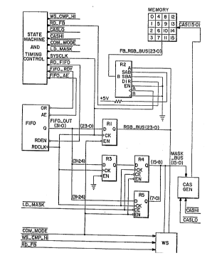
The frame buffer system shown in Fig. 4 comprises a state
machine 50 which provides both address and timing control
signals on its output lines. State machine 50 is
essentially a sequencer that is organized by a central
processor (not shown). The system further includes a FIF0
store 52 which feeds into registers R1, R2, R3, R4 and R5.
Compressed data is fed to FIF0 52 via data in cable 54. A
CAS* generator 56 has applied thereto bit MASK portions from
registers R4 and R5 and a pair of control signals CASHI* and
CASL0*. A workstation 5~ is also interconnected with CAS*
generator 56 and register R2 to enable a workstation 58 to
also access frame buffer 32. Frame buffer 32 is organi~ed
as shown in Fig. 3 and comprises a 4x4 matrix of modules
M0-M15.
In Fig. 5, details of CAS* generator 56 are shown. Sixteen
multiplexers (MUXl through MUX16) receive CASL0* and CASHI*
input levels. As will become apparent hereinafter, the
CASL0* and CASHI* levels become active at different times in
a single memory cycle. In addition, a bit level from the 16
bit MASK pattern is applied to each multiplexer as a
controlling input and causes the respective multiple~er to
provide an output upon the occurrence of the active state of
one of its controlling inputs. If the MASK input is a 1,
the respective MUX selects CAS~I* and if the MASK input is a
0, the respective MUX selects CASL0*. Since CASL0* and
Y09-91-093 11 ~ L
CASHI* levels become active at different times in the cycle,
16 CAS* levels are produced on output cable 60 in a single
memory cycle. Each CAS* level controls the writing of a
color value into a respec-tive pixel position of one of ~he
16 pixels within the 4x4 pixeL matrix.
For the simplicity of description the HI color write will be
described as preceding the Lo color write for a given set
of compressed data. This is not, however, a limitation of
the invention, since either order can be used.
The method to be described hereafter for generating CAS*
signals allows an 80 nS decompression cycle. The me~hod
reduces the time it takes to activate two CAS signals,
CASHI* and CASLO*, where CASHI* is used to load the HI color
and CASLO* is used to load the LO color. All HI colors of a
compressed data set are stored into VRAMs using the same row
and column addresses and are loaded during a CASHI* active
time in a single memory cycle. When CASLO* becomes active
later in the same memory cycle, all LO colors are loaded,
thus enabling 16 pixel positions to be loaded with both
colors in a single memory cycle.
Figure 6 shows a typical timing diagram specified for a
VRAM. The timing information is from a Mitsubishi, 1 Mbit
VRAM part number MSM442256JL-8. This timing information
determines the performance of the frame buffer.
* tpC ~ East Page Mo~e Cycle Time. Minimum of 50 nS
* tcaS - CAS -Pulse Width. Minimum of 25 nS.
* tcp - CAS-Precharge Time for Fast Page Mode. Minimum of 10
nS.
*. tdSC - Data Setup Time. Minimum of O nS.
* tdhC - Data Hold Time. Minimum of 25 nS.
* t - Column Address Setup Time. Minimum of 5 nS.
asc
* tcak - Column Address Hold Time. Minimum of 20 nS.
Fig. 7 shows the timing diagram of a fast compressed mode
page mode cycle used by this invention. A less than lOOnS
(2tpc) cycle is achieved using a VRAM with tpc of 50 nS. As
shown in the timing diagram, CASHI* and CASLO* signals can
Y09-91-093 12
be overlapping. This is possible, since for a compressed
mode memory cycle, only one CAS~ is selected, whether it be
CASHI* or CASL0*, but not both at the same time. M HI and M
L0 on the DATA Line indicate when the ~I and L0 colors are
manifested by register R2 in a memory cycle. The minimum
possible cycle time for decompression is, TCmp = t1 + t2,
where t1 is tdhC (Data hold time) and t2 is tpc (Page Mode
Cycle).
It should be noted that tl is necessary so that data hold
time for the first color write cycle is not violated. Time
t2 is necessary due to the memory operation where a memory
module has a L0 color compressed mode followed by a HI color
compressed mode. The separation between these two
consecutive CAS* falling edges must be at least tpc.
As indicated above, a Mitsubishi, 1 Mbit VRAM exhibits a,
tdhC=25 nS and a tpC=50 nS. Thus ideally, tcmp=75 nS. With
75 nS decompression, HPPI compresssd data can be received at
full transfer rate. Since the -time required for a
decompression is reduced from 100 nS to 75 nS, the
performance improvement due to the two CAS method is,
R2cas=100/75-1-33-
In order for the frame buffer not to be a networkbottleneck, the relationship T ~ NP must hold true, where T
is the throughput of the network, N is the number of 4x4
memo~y modules interleaved, and P is the performance of the
frame buffer decompression for a 4x4 memory module. For
HPPI, T = 200 million pixels/second. If a two CAS* method
is not used, then with a single 24 bit R, G, B data path,
each decompression takes 100 nS with a 50 nS VRAM. This
results in P = 160 million pixels/second. Therefore, in
order for the frame buffer not to be the bottleneck, N must
be >= 2. Another 4X4 memory module is needed which operates
in parallel. Alternately, an expensive method of
interleaving, where each memory module has its own separate
data path and controls may be used. However, if a two CAS*
method is used, then P = 213 million pixels/second can be
achieved. Therefore only one 4X4 memory module with only a
single 24 bit R, G, B data path is needed.
YO9-91-093 13 ~ ~ ~P~
Referring now back to Fig. 4 in conjunction with ~ig. 7, the
operation of the on-line decompression/buffer system will be
described. Succeeding 32 bit data words are fed via data
input 54 into FIFO store 52. A free running system clock
(SYSCLK) is generated by state machine 50 and controls the
operation of FIFO 52 as well as synchronizing the remaining
components of the system.
When enough data has been received in FIFO 52, the FIFO RD~*
signal i5 activated to signify that there is data in FIFO 52
to be processed. State machine 50 recognizes that signal
and enters the fast page memory access mode by activating
communication mode signal COM MODE* and RD FIFO* until it
aborts the fastpage memory mode access upon detecting FIFO
almost empty (FIFO AE*). State machine 50 also generates a
load MASK enable signal (LD MASK*) every second SYSCLK for
the duration of RD FIFO*. Note that since the compressed
data always comprises a pair of 32 bit words, the duration
of RD FIFO* is always a multiple of two S~SCLKs.
24 bit color data (23:0) is read out of FIFO 52 and piped to
registers Rl and R2. HI MASK bits (15:8) are also read out
of FIFO 52 and are temporarily stored in register R3 for a
clock period and are then loaded into register R4 on the
same clock period when LO MASK bits (7:0) are loaded into
register R5. The 16 MASK bits (15:0) are held in registers
R4 and R5 while HI and LO color data bits are successively
loaded into register R2 and are driven into memory modules
32.
Memory 32, as described above, is configured with 4x4 memory
modules, with pixels interleaved therein in both the
horizontal and vertical directions in a 4x4 pattern. CAS*
generator 56, in a memory cycle, provides 16 CAS* signals
whose levels are controlled by the color MASK. During the
first portion of a decompression cycle (i.e. CASHI*), a 24
bit HI color is broadcast from register R2 to memory modules
32, and CAS* generator 56 generates active levels on those
of its output lines that correspond to bit positions
exhibiting a 1 level in the bit MASK. This enables the HI
color data to be written in parallel into selected pixels
2 ~ ~ ~7 ~
YO9-91-093 1~
corresponding to the high order MASK bit positions that are
at the 1 level. On the second part of the decompression
cycle (i.e. CASL0*), the L0 color pixels are written under
control of the 0 bits in the bit MASK, thus completing a
decompresslon cycle.
The above operation is partially illustrated in Fig. 7
where, when CASHI* drops to the active state, 1 bits in the
MASK cause CAS* signals to be applied to memory 32 so that
the HI color bits emanating from register R2 are written to
the 16 pixel memory positions. In a similar manner, when
CASLO* drops to the active level, the LO color bits are
written to the pixel positions corresponding to the 0 bits
in the MASK.
Workstation 58 (see Fig. 4) also has access to buffer memory
32 via busses 60 and 62. Through appropriate imposition of
MASK bits on bus 60 and color data on bus 62, the CASHI* and
CASL0* signals can achieve the writing of the color data
into memory modules 32, as above noted.
When a very high resolution frame buffer is desired, the
video clock rate cannot be ignored. For example, a VRAM has
a serial port which can be operated at 33 Mhz. But, for a
60 Hz, 2048 x 1536 resolution monitor, the video clock speed
is in excess of 260 Mhz. It can be seen that (260 Mhz / 33
Mhz) = 7.88. In order to match the video clock, the VRAM
must be interleaved a minimum of 8 ways to provide enough
serial output bandwidth for the high resolution monitor.
The design shown in Fig. 4 is modular and the video OUtptlt
bandwidth can be increased to 4P of a single VRAM serial
output, where P is a positive integer which represents the
number of 4x4 sets of memory modules beinq used. This
allows the system s video throughput to be increased to
match any resolution monitor. A 60 Hz, 2048 x 2Q48
resolution monitor requires a 360 Mhz video rate. Since
(36Q/33)=10.9, then P=3 would provide enough video
bandwidth.
As shown in Fig. 8, this can be done by adding more 4x4
memory modules onto the main bus. A module consists of
Y09-91-093 15
CASGEN* and a frame buffer (FB). The 4x4 memory elements
themselves are interleaved. In other words, a first module
will have pixels 0 through 3, a second module will have
pixel~ 4 through 7, until a j-th module which will have
pixels 4(j-1) through 4(j-1) ~ 3. The controlling state
machine (SM) must be modified in a way that it selects the
correct CASGEN* and frame bu~fer when memory requests are
made. Using this modular 4x4 approach, a video output
throughput can be extended indefinitely to match any video
rate for any monitor.
When the design requires interfacing to an even higher
bandwidth communication network, it can be modified to
accept higher throughputs from the network by parallelizing
the input. This can be done by adding more FIFO's,
CASGEN's, and FB's with a slight modification to the
existing SM. Figure 9 shows an example, where there are
three sets of FIFO's, CASGEN's, and FB's. With this
arrangement, there will be parallelization among three
modules to increase the performance by a factor of 3. Due
to the modular approach, the number of FIFO's, CASGEN's, and
FB's added can be increased indefinitely to match any
network bandwidth.
The resolution of the frame buffer can also be extended.
For example, if each memory module is designed using 1
million bit VRAMs, each of which is configured as 512 rows
by 512 columns by 4 bits each, then the 4xg memory modules
are configured as 2048 rows by 2048 columns by ~ bit-planes.
This can be extended to match any system requirement.
First, increasing bit-planes per pixel can be done by adding
m~re VRAMs. For example, if a 30 bit R,G,B data format is
used, then eight 1 Mbit VRAMs per memory module can be used
(this configuration can provide up to 32 bit-planes).
Although 2048 x 2048 resolution frame buffer is adequate for
the most applications, there are situations such as double
buffering, real-time panning, or higher resolution monitors
where even larger frame buffer configurations are needed.
The invention may be extended indefinitely in both
horizontal and vertical directions to accommodate any size
2 ~
Y09-91-0~3 16
frame buffer. If the frame buffer needs to be extended
horizontally, then more 4x4 modules can be added
horizontally as shown on Fig. 10, where ther~ are P 4x4
memory modules horizontally which provide a total of 2048P
horizontal pixels. I* the frame buffer needs to be extended
vertically, then more horizontal rows of P 4x4 modules can
be added vertically, as shown, where there are N 4x4 memory
modules vertically which provides a total of 2048N vertical
pixels.
It should be understood that the foregoing description is
only illustrative of the invention. Various alternatives
and modifications can be devised by those skilled in the art
without departing from the invention. Accordingly, the
present invention is intended to embrace all such
alternatives, modifications and variances which fall within
the scope of the appended claims.