Note: Descriptions are shown in the official language in which they were submitted.
2~7:~3
E~GE INTEGRATIN(: P~SE DETECTOR
~L~
The present in~rention relate to phase losked loops,
and more particularly ~o an e~ge integrating phase
detector for ~ phase lock loop that acts to minimize
j itter due to nois~ of a l~iming system derived from an
input signal while maintaining a relatively large
bandwidth in ~:he system to respond t: timing variations
in ~h~ input signal.
In a raster scann~d video system a video waveform
has a repetitive reference component, referxed to as
sync~ hat is used to generate timing for the s~stem. To
generate this timing it is necessary to lock a local
oscillator to the sync component so that all processing
within the system occurs at ~OWTl ti:ming relationships
with the video waveform~ Commonly a phas~ locked loop is
used that compares the phase o:e a referencP clock to a
sync signal derived from l:he sync component and adjusts
th~ frequency of the re~erencs clock until the phase
2 O between the two signals has a E3red~termlnPd value .
Typically tha video waveform is input to a sync stripper
that provides the derived ync slgnal a~ a train of
pulses, each pulse having a leading edge corresponding to ~.
a timing reference point on the video wave~orm. ~he syna
stripper compares the video waveform with a fixed level,
with the l~ading edges of the pulses in th~ derived syn ::
signal occurring when the virleo waveforr~ le~el crosses
the fixed level in a gi~ren directioII. Noise in the video
wave~orm causes this crossing point to vary on a random
3 O basis, producing j itter in the derived sync signal .
The derived syns:~ signal is input to a phase detector
to~ether with a clos~k signal derived from the video
system cloclc. The difference in phase between the
appropriate clock signal ed~e and the correspor~d~ ng sync
signal edge is converted into an error voltage that is
applled to the syste:n c:lo;::k to ad~ust its ~requency until
the phase dif ference achiev~s the predetPrmined value .
. .
2Q~ at?~
If there is noi.e on the video waveform that caus2s
jitter in the derived sync signal, as described above the
period between the pulses of the deri~ed sync signal
vary, and there is a constant correcting o~ the syste~
clock such that the phase locked loop output has jitter
relative to the input signal. To reduce this jitter
effect due to noise, a loop filter having a very low
bandwidth is in~erted into the pha~e l~cked loop so that
only an average variation in the period between pulse~
affects the timing of the phase locked loop. The low
bandwidth loop ~ilter, while ef~ectively reducing jitter,
reduces the response time to variations in the reference
~ync signal.
What is desired is a phase locked loop that reduces
jitter due to noise on a video waveform while maintaining
the ability to respond rapidly to variations in the video
wave~o~m.
8 D ary of the Inve~t~on
Accordingly the pre~ent lnvention provides an edge
integrating phase detector for a phase lock loop that
reduces jitter due to noise on an input video waveform by
integrating an edge o~ a sync pulse contai~ed with~n the
video waveform. Th~ input video waveform is buffered and
input to a gated sampling circuit that passes the edge,
or transition, of the sync pulse to an intagrating
circuit. A gate signal ~or the gated sampling circuit is
derived from a system clockO The output o~ the
integrating circuit is input to an error amplifier
together with a refe~ence ~ignal that represents the
timing reference level of the sync pulse to produce an
error signal that i~ fed back to control the freguency o~
th~ system clock~ and thus the position Qf the gate
signal relative to the sync pulse edge~
The objects, advantages and other novel ~eatures o~
3S the present invention are apparent from the following
~7~e~
detailed description when read in conjunction with the
appended claims and attached drawing.
Brie~ De~¢riPtion of t~e Drawl ng
a, i
Fig. 1 is a block diagram of~phase locked loop -~~~
incorporating an edge integrating pha~e d~tector
accordlng to the present invention~
Fig. 2 is a simpligied ~chematic diagram o~ the edge
integratlng phase dete~tor according ~o the present
invention. -~
Fig. 3 i~ a ~implified block diagram of a gat~
generator for the edge integrating phase detector
according to the present invention.
Fig. 4 is a timing diagram for the phase locked loop
incorporating the edge integrating phase detector
according to the present invention.
De~ri~ti~n o~ the preferred E~bod~ment
Re~erring now to Fig. 1 a pha~e locked loop 10 is
shown having a vol~age controIled o~cillator (VCO) 12
that provides a syst~m clock signal CLO~R. An input
signal ~ having a repetitive component~ such as a video
signal having a ~ync component, is input to a buf~er
ampllfier 14, the output of which i~ coupled as an input
to an edge integrating pha~e detector ~6. Also coupled
as an input to the edge integrating phase detector 16 iæ
a gate strobe ~ignal B. ~h~ gate strobe signal B is
producad by a gate generator 1~ that receive~ a~ an input
the clock signal. The input signal is integrat~d by the
edge integrating phase detector 16 during th~ gate strobe
signal B. The integratsd æesult from the edge
integrating phase detector 15 is input as an esse.ntlally
d.c~ signal to an error a~plifier ZO that includes a loop
filter. The d.c. signal is compared in the error
amplifier 20 with a re~erence voltage ~B~ that
2~7~
corresponds to the appropriate voltage level for the
timing reference point of the input signal. For an HDTV
video slgnal the voltage level for the syn~ point is
ground, while ~or an NTSC video signal the voltage level
for th~ sync point is -20 IRE. The output of the error
amplifier 20 is an error signal that is applied to the
VCO 12 to ad~ust the frequency of the VC0. The
integration o~ the sync edge essentially removes jitter
due to noise so that the loop ~ilter of the error
lo amplifier 20 may hav~ a higher bandwidth, i~e., on the
ord~r of 50 times higher, than prior art loop filters,
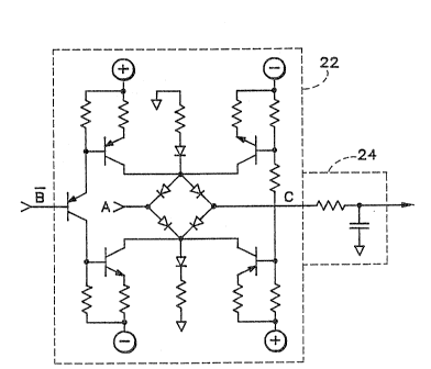
As sho~n in Fig. 2 the gate ~trobe signal B, or its
inverse \B, is input to a sampling circuit 22. Also
input to the sampling circuit 22 is the input signal A.
~t ~he ou~put C of the sampling circuit 2~ the portion of
the input signal A captured during the gate strobe signal
B is passed to an integrating circuit 24~ ~ny suitable
integrating circuit may be us~d, and in i~s mos~
~implistic form i an RC circuit as shown. The
inte~rating circuit ~4 in~egratss about the sync point so
that there is a negative and positive portion at the
input. For lock the negative and positive portions are
egual, i.e~, the gate strobe signal B i~ cent2red about
the sync point, and the output of the integrating circuit
24 is at the reference level so that the output of the
error amplifier 20 does not change the VCo 12 frequency.
The gate strobe signal generator ~8 is shown in Fig.
3 as having a counter 26 and a decoder 2~. The counter
26 counts the pulse~ of the clock signal CLOC~ fxom the
VC0 12. The cou~t from the counter 26 is input to the
decoder 28 that provides the leading edge of the gate
strobe signal B when the count reaches a predetermined
value that is a function of the format of the input
signal. If the phase locked loop 10 is locked, then the
leading edge of the gate strobe signal B occurs shortly
after the start of the transition of the sync edge from
one level to another. The decoder 28 holds the gate
.:. : ,.
2 ~ ~ 7 r~ 9 3
stro~e signal B for a range of counts from th~ counter 26
corresponding to a predetermined number of pulses of the
clock signal CLOC~.
In operation a~ shown in Fiy~ 4 an HD~V video signal
~ has a tri~level sync pattern with the sync point x
occurring at the middle of the rising tran~ition. The
gate strobe signal B turns on the sampling c~rcuit 22 and
allows a portinn c o the ~ync signal to dri~e the
integrating circuit 24. As shown in thts example the
gate strobe sig~al B is late so that the lntegrating
circuit 24 receives unequal positive and negative inputsn
The output of the integrating circuit 2~ is proportional
to the input unbalance, a~d thus through the error
ampli~ler 2Q dri~es the VCO ~2 to correct the gate stro~e
signal timing4 N ~ e that occurs within the gate strobe
period is integ~a ~ and has little effect on the timing of ~-~~
the phase locked~op lo.
For a particular H~TV television application the VC0
12 may have a range of ~reguencies between 68 78 MHz.
The rise time o~ the sync Pdge of the HDTV video signal
is approxi~ately 50 ns, while the faIl time o~ the sync
edge o~ an NTSC video signal ic approximately 140 ns.
The strobe width of the gate strobe signal B preferably
is less than the transition times of the sync edges,
i.e., strobe widths o~ 40 ns for HDTV and 110 ns for
N~SC, but it may be longer so long as the width is
substantially filled by the transition so that the error
signal is essentially the integral of the sync edge
transit~on. Also a variable delay circuit, su~h as that
described in Research Disclosure August 1990, pages 633-
634, may be inserted in the gate strobe si~nal path to
provide more precise timing for ~arying the phase of the
~ystem clock CLOCR relative to the input signal.
Thus the present inventlon pr~vide~ an edge
integrating phase detector for a phase loc~ed loop that
lntPgrates the transition of a repetitive component in an
input signal in order to generate an error signal for
controlling the phase of a clock osciliator relative to
the repetitive component while minimizing the effect o~
noise on the phase locked loop.
: . .
:
: ~ . :