Note: Descriptions are shown in the official language in which they were submitted.
2~799~
The present lnventlon used ln a multl-colour
prlntlng machlne refers to a devlce for scannlng varlous
colour marks prlnted by varlous prlntlng unlts, the sald marks
allowlng subsequently to determlne mlsreglster of lts
pertalnlng colour wlth regard to the colour prlnted by the
flrst prlntlng unlt and used as reference.
Known devlces such as the one descrlbed ln European
Patent No. 0 094 027 publlshed 16 November 1983 operate to
satlsfactlon provlded that the yellow, blue or red marks are
sufflclently contrasted for belng recognlzed lnfalllbly by the
scannlng devlce. Some of these known devlces may operate wlth
a flbre optlc llght beam hlttlng the prlnted workplece and
dlrectlng the reflected llght onto a scannlng photodlode
produclng an electrlc slgnal. In order to enhance the
contrast between the electrlc baslc slgnal, correspondlng to a
non-prlnted area of the workplece, and an electrlc lmpulse
produced by the passlng mark, a fllter, usually of blue
colour, ls lnstalled between the flbre optlc and the
photodlode.
However, as soon as the prlnted colours fade to
paleness especlally so when prlntlng packages wlth pastel
yellow, cream or llght blue, the conventlonal devlces are no
longer capable of detectlng safely the varlous prlnted marks
so that the one or the other reglster control mlght fall to
operate correctly. In such cases, lt mlght be approprlate to
use a flrst fllter, to present a pale colour ln order to test
the quallty of the slgnal obtalned and to repeat the test wlth
one or several other fllters so as to select the one most
approprlate for all
- 1 - ~
68200-127
' 3t
2067994
68200-127
marks. However, the most important phase of the start-up of a
printing machine consists in searching the initially unknown
position of a concomitant mark, which, though, cannot be reliably
carried out without an immediately responsive scanning device.
Such numerous, and indispensible, tests become quickly inhibitive
if the printing machine is to be used for accomplishing a great
number of different jobs.
The purpose of the present invention is the creation of
a detector spotting printed marks whatever their colour, intensity
and contrast with regard to the background colour of the flat
workpiece it is printed on.
These purposes are attainable by means of a device
scanning printed marks since it comprises at least two parallel
mark scanning channels each of which emits an electric impulse
each time the mark travels through under the light source, the
photosensitive unit at the input of the two channels being respon-
sive to a colour frequency range distinguishable from the others,
as well as electronic means selecting the most representative
mark impulse among the electric impulses emitted by the channels.
Appropriately, every mark scanning channel comprises:
- a photosensitive unit generating an electric signal for
the voltage value, followed, if required, by
- an amplifying stage with automatic gain, fixing at a
predetermined rate the basic voltage corresponding to a non-
printed area of the workpiece, followed by
- a stage converting the oblique sloped electric
2067994
68200-127
impulse called forth by the mark travelling under the photosen-
sitive unit into a steep sloped electric impulse, every steep
slope corresponding to the beginning of the ascent or descent of
the associated oblique slope,
- and electronic means selecting among the electric
impulses originating from the channels at a given moment the
impulse appearing or disappearing first.
Hence, owing to this device, the electric impulse with
the strongest contrast is regularly retained whatever the quality
of the other impulses considered.
A by-problem, however, might somewhat complicate the
conception of the selective circuit since a colour mark printed
on a white workpiece will bring forth a negative impulse with
regard to the basic signal whereas a very reflective, say gold
or silver, colour mark, will bring forth an inverted, i.e. posi-
tive, impulse with regard to the basic signal. This problem is
obviated in that every scanning channel additionally includes
before the converting stage a rectifying stage imposing on all
electric impulses a variation in the same direction with regard
to the basic voltage.
Appropriately, the photosensitive unit includes a photo-
diode situated behind a tinted filter and connected to the input
of a current/voltage converter.
In accordance with a preferable mode of realization, the
rectifying stage includes a first stage for rating the basic
voltage, followed by a stage for subtracting the basic voltage
2~67994 68200-127
thereby leaving only positive or negative impulses, followed by
a stage for rectifying solely the positive impulses into
negative ones, followed by a stage for adding all the impulses
and, finally, followed by a stage ensuring the re-addition of the
basic voltage.
In accordance with a preferable mode of realization, the
converting stage includes a first stage for detecting peaks,
followed by a second stage for subtracting the input signal from
the threshold detected by the first stage, the difference being
applied to a comparator which switches its output as soon as the
difference exceeds a predetermined threshold, as well as the
first electronic means re-initializing and inverting the detection
direction of the peak detecting stage as well as the second elec-
tronic means inverting the polarity of the comparative threshold
applied to the comparator after a first switch of the latter.
In accordance with a preferable mode of realization, the
electronic means for impulse selection include a first OR gate
receiving one of the impulses at both of its inputs and whose out-
put is connected to the clock input of a first bistable device and
as many secondary bistable devices as there are impulses to be
analysed, the said impulses being received inverted at their
clock input, all the inverted outputs of the secondary bistable
devices being connected to the input of an AND gate whose output
is connected to the re-initialization input of the first bistable
device, the re-initialization input of every secondary bistable
device being connected to the non-inverted output of the first
2Q67994 68200-l27
bistable device, and a final line for monitoring electronic means
being connected to one of the inputs of the AND gate.
In accordance with an appropriate mode of realization,
the device includes, moreover, an analog/digital and digital/
analog converter connected to a micro-processor destined to
receive from the rectifying stage the basic voltage valve and to
feed, on the one hand, the amplifying stage with automatic gain,
if present, with an electric signal representative of the gain to
be applied and, on the other hand, the converting stage with an
electric signal representative of the threshold which is optimal
for the comparator. Owing to this latter device, the voltage is
permanently held at a rate of about 8 volts, and the comparator
detection threshold is fixed at a rate between 200 and 400 milli-
volts above the average noise emitted with the basic voltage.
The invention will be better understood by examining a
realization mode selected as a non-limitative example described
below in conjunction with the attached drawings, in which:
- Figure 1 is a schematic diagram of the device according
to the invention,
- Figure la is a partial view of a particular execution of
the device according to the invention,
- Figure 2 is a lay-out of the rectifying circuit operat-
ing in the device of Figure 1,
- Figure 3 is a lay-out of the converting circuit
operating in the device of Figure 1,
- Figure 4 is a diagram of the operation carried out by
2 0 6 79 9 4 68200-127
the converter of Figure 3, and
- Figure 5 is a lay-out of the selective circuit operating
in the device according to Figure 1.
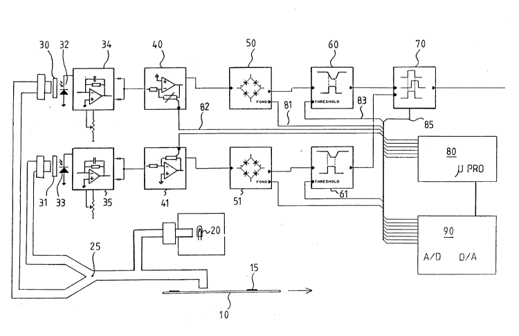
As illustrated by Figure 1, the device according to the
invention includes a fibre optic bundle 25 initially transmitting
the light emitted by a light source 20 above the printed work-
piece 10 provided with colour marks 15 printed on its upper side.
These workpieces might be paper strips or cardboard plates
undergoing a manufacturing process. Such marks 15 are printed
in an unrestrained area of the workpiece and with the colour
printed by each printing unit. The passage of these marks 15
under the input of the fibre optic bundle temporarily modifies
more or less the reflected light which, after doubling of the
fibre optic, is transmitted to two separate photodiodes 32, 33.
According to the invention, the photodiodes 32, 33 are
each rendered sensitive to distinct colours by means of filters
30, 31 situated between the outputs ofthe fibre optics and the
photodiodes. So, for instance, the filter 30 can be dark violet
enhancing yellow marks whereas the filter 31 is green enhancing
blue marks. The electric signals emitted by each photodiode are
initially conditioned separately and parallelly by identical
processing channels consisting of the circuits 34, 40, 50 and 60,
and then compared by a selective circuit 70.
These identical and parallel conditioning channels each
include a current/voltage converter 34 producing a voltage
variation from the intensity variations occurring within the
2 0 67 9 9~ 68200-l27
photodiode and caused by the mark 15 passing under the fibre optic
input. As symbolically represented, this current/voltage
converter is made in a known way of an operational amplifier with
feedback between its output and its negative input. Clamps
symbolically shown at the output allow to put in operation a first
or a second feedback circuit, thus modifying the gain of this
stage in a relationship of 1 to 10. This voltage signal is then
amplified by an amplifying circuit with automatic gain 40 in
such a way that the basic signal corresponding to a non-printed
area of the workpiece 10 will be fixed at a value of 8 volts.
This explains why, according to the background colour of the
printed workpiece 10, to the length of the fibre optic bundle 25,
to possible dust particles likely to alter the input or the output
of the fibres as well as the filters, the basic voltage received
at the output of the current/voltage converter 34 may vary between
150 millivolts and 8 volts.
The electric signal then flows into a rectifying circuit
50, the purpose of which is to gather all colour mark impulses in
an identical direction which in the present case is negative, with
regard to the basic voltage. In most cases, the marks 15 are
printed with colours darker than the background colour and thus
cause a reduction of the light reflected on the fibre optic, i.e.
an instantaneous reduction of the current flowing through the
photodiode 32 or 33, in other words an impulse with a lower vol-
tage than the basic voltage. Inversely, if the marks 15 appear
brighter than the background colour or if they are printed with
-- 7
2067994 68200-127
particularly reflective colours such as gold or silver, the
reflected light is temporarily stronger than the basic light and
the same effect affects the corresponding electric impulse. By
making all impulses have a common polarity, this rectifying cir-
cuit allows to considerably simplify the subsequent selective
circuit.
Figure la represents a device similar to the one of
Figure 1 in which the fibre optic 25 has not been doubled. A
light diffusion device 25a has been added to the end of the fibre
optic 25 so that the reflected light will be indifferently
directed to the filters 30 and 31. The design of the other
components of the device including the photodiodes 32 and 33 as
well as the current/voltage converters 34 and 35 remains unchanged
with regard to the lay-out shown by Figure 1.
If reference is made to Figure 2, this rectifying
circuit 50 includes a background rating stage 51, followed by a
background subtracting stage 53, followed by the actual rectify-
ing stage 55, followed by an impulse adding stage 57, terminated
by a background re-adding stage 59.
As illustrated, the background rating stage 51 essential-
ly includes the combination of a diode 513 and a capacitor 514
the other line of which is grounded. The operational amplifiers
511 and 512 act as isolators of the stage. By temporarily short-
circuiting the diode 513, the switch 515 allows to periodically
re-initialize this background rate.
The subtracting stage 53 includes in a known way an
2067994 68200-127
operational amplifier 533 receiving the complete signal through
the resistor 531 on its positive input as well as the background
value to be subtracted through the resistor 532 at its negative
input.
At the rectifying stage 55, only positive impulses are
amplified and inverted by the operational amplifier 553 compris-
ing two diodes 551, 552 in its feedback circuit. The addition,
by the operational amplifier 573, of the adding stage 57, fed
through its negative clamp with the signal originating directly
from the subtracting stage 53 through the resistor 571 as well as
with the amplified negative impulses used for balancing the
positive impulses, provides at the output of this stage a sequence
of impulses of the same amplitude as initially, though with all
impulses in the negative direction.
The operational amplifier 593 of the re-adding stage
59 adds the background value transmitted direct from the first
background rating stage 51 through the resistor 591 and the
impulses emitted by the adding stage 57 through the resistor 592.
If reference is made to Figure 1, the rectifying circuit
50 is followed by a circuit 60 converting the oblique-sloped
impulses into steep-sloped ones which latter provide easier
subsequent logical processing.
As illustrated on Figure 4, the impulses el and e2
generated by the photodiodes 32 or 33 show a first descending
oblique slope corresponding to the progressive penetration of the
mark into the fibre optic scanning area, followed by a bottom
g
20~799~ 68200-127
level appearing with the mark body passing, and terminated by a
second ascending slope corresponding to the mark leaving progres-
sively the scanning area.
The detailed structure of this converter 60 will be
described in connection with Figure 3 on which four important
stages are distinguishable, i.e. a peak detecting stage 61,
followed by a stage 62 for subtracting the measured peak from the
instantaneous signal, followed by a stage 63 for comparing the
difference with a predetermined threshold originating from a
stage 64. The result of this comparison is shaped by the opera-
tional amplifier 632 the inverted signal of which is generated by
the inverter 633. The output of the shaping amplifier 632 is
also used as a counter-reactive item destined to invert the
direction of the maximum detection rate of the stage 61 and to
modify the threshold rate originating from the stage 64.
The peak detecting stage 61 essentially includes a
diode 614 (and then 615) acting jointly with a capacitor 613
whose input is controlled by the amplifier 611 and whose output
is controlled by the operational amplifier 612. The direction of
the maximum detection rate, either in the ascent or descent,
is initially determined by the state of the relay 65 selecting
either diode 614 or 615. This stage is re-initialized by the
relay 644 after a short period added by the inverter 633 by means
of the diodes 616 or 617 depending on the case.
The subtracting stage 62 receives the signal originating
from the peak detecting stage 61 through the resistor 621 as well
-- 10 --
68200-127
206799~
as through the resistor 622, the instantaneous signal previously
amplified by the operational amplifier 619 with a gain of 1. The
comparison is ensured by the amplifier 631 receiving the threshold
signal at its positive input and the difference signal at its
negative input.
As may easily be gathered from Figures 3 and 4, the
stage 61 firstly receives the rate of the basic voltage, whereas
the output of stage 62 firstly provides a zero signal which is to
increase only with the appearance of the descending oblique slope
of an impulse. If the oblique slope of this impulse exceeds a
predetermined threshold vl with regard to the basic voltage, the
output of the operational amplifier 631 will switch and a first
steep voltage ascent sll will appear at the output of the inverter
632. This voltage ascent sll begins by causing the selection of
the diode 615 enabling the capacitor 613 to be discharged through
the diode 617 and then the diode 616 to be connected after a
period to be determined by the inverter 633. The stage 61 is then
ready for detecting a new maximum though in the descending
direction. The first voltage ascent has also caused at the stage
64 a modification of the threshold voltage v2 by grounding the
positive input of an operational amplifier.
The stage 61 then detects the rate of the lower bottom
level of the impulse el, whereas the output of the subtracting
stage 62 remains at zero as long as the bottom level lasts. Once
again, with the appearance of the beginning of the ascending
oblique slope of the inlet impulse, the difference at the outlet
68200-127
206~99~
of the stage 62 will increase and even exceed the new threshold
v2 of the comparator 631 which then will invert its output signal,
thereby causing a sudden descent s12 of the output of the shaping
amplifier 632.
In this way, the steep ascending slope of the output
impulse sl corresponds more or less to the beginning of the
descending oblique slope of the input impulse el, whereas the
steep descending slope of the output impulse sl corresponds more
or less to the beginning of the reascending oblique slope of the
input impulse el.
As may be gathered from Figures 1 and 4, the impulses
sl and s2, now castellated, respectively emitted by the channel
corresponding to the yellow colour and the channel corresponding
to the blue colour are applied to the selective circuit 70
retaining the ascending impulse sl which will descend first and
correspond to the initial oblique slope of the most contrasted
impulse el.
The mode of realizing the circuit 70 as illustrated by
Figure 5 includes a first OR gate "OU" 71 receiving one of the
castellated impulses at both of its inputs and whose output is
connected to the clock input "CLK" of a first bistable device 72.
The selective circuit 70 includes as many secondary bistable
devices 73, 74 as there are impulses to be analysed, these im-
pulses being received inverted, i.e. at their clock input "CLK".
All the inverted outlets "Q" of the secondary blstable devices are
connected to the input of an AND gate "ET" 75 whose output is
- 12 -
2067994 68200-127
connected to the re-initialization input'!-CL"of the first bistable
device 72. Moreover, the output "Q" of this first bistable
device 72 is also connected to the re-initialization input "CL" of
each of the secondary bistable devices 73, 74. A last permitting
or interlocking line 85 of the selective circuit 70 is connected
to one of the inputs of gate "ET" 75.
At the initial state of the device, all inputs of the
gate "ET" 75 are high, thus releasing the first bistable device
72 whose output "Q" is initially low, entailing the interlocking
of the bistable devices 73 and 74. With an impulse reaching one
of the inputs of the OR gate 71, the output of this gate is high,
resulting in the appearance of a high signal on the output gate
"Q" of the bistable device 72, which latter brings about the as-
cending slope of the output impulse and also releases the bistable
devices 73 and 74. The arrival of the ascending slope of the
second impulse then has no more effect on the circuit 70. On the
other hand, the arrival of the first ascending slope of an inver-
ted signal, corresponding actually to the descending slope of
this first impulse, will change the state of the corresponding bi-
stable device 73, 74 resulting in the immediate lowering of the
corresponding output "Q". The gate "ET" 75 will have at least one
of its inputs forced low, whereas its output also lowers resulting
in the re-initialization of the first bistable device 72, and
putting the corresponding output "Q" back to low, thus creating
the descending slope of the output impulse. This low signal
at the output "Q" of the bistable device 72 also results in the
- 13 -
2067994 68200-127
re-initialization of all secondary bistable devices 73, 74 putting
all inverted "Q" outputs high and thereby interlocking these
bistable devices and preventing the ascent of the subsequent
inverted signal. The output of gate "ET" 75 returns to high,
which action again releases the bistable device 72 and renders it
suited for the subsequent selection as long as a permission to
that end is maintained on the line 85.
As may be gathered from Figure 1, the device according
to the invention includes moreover an analog/digital and digital/
analog converter 90 acting jointly with a micro-processor 80, this
device being capable of receiving on line 81 a value of the basic
voltage in order to return to the lines 82 an electric signal
corresponding to the gains to be applied to the amplifying cir-
cuits 40 and 41 with automatic gain, and to the lines 83 a
threshold rate for the comparator 63 of the circuits 60 and 61, the
said threshold being fixed between 100 and 400 millivolts above
the background noise measured on the basic signal. The micro-
processor also transmits to the line 85 a monitoring signal
interlocking the selective circuit as long as no mark is awaited.
As may be gathered from the aforesaid comments, the
device according to the invention allows to reliably detect a
mark travelling through a light beam emitted by the source 20, the
said device effectuating an instantaneous selection of the best
suited scanning channel for yellow or blue, simultaneously taking
into account the colour, the contrast and the intensity of the
mark to be considered. For machines expected to carry out
- 14 -
206799~ 68200-127
delicate jobs, it is quite possible to add a third or fourth
parallel scanning channel for other well distinguishable colours.
Numerous improvements may be added to this device within the
limits of the invention.